EP0965654A2 - Verfahren zur Erzeugung metallhaltiger Schichten - Google Patents
Verfahren zur Erzeugung metallhaltiger Schichten Download PDFInfo
- Publication number
- EP0965654A2 EP0965654A2 EP99109894A EP99109894A EP0965654A2 EP 0965654 A2 EP0965654 A2 EP 0965654A2 EP 99109894 A EP99109894 A EP 99109894A EP 99109894 A EP99109894 A EP 99109894A EP 0965654 A2 EP0965654 A2 EP 0965654A2
- Authority
- EP
- European Patent Office
- Prior art keywords
- metal
- layer
- titanium
- metal layer
- layers
- Prior art date
- Legal status (The legal status is an assumption and is not a legal conclusion. Google has not performed a legal analysis and makes no representation as to the accuracy of the status listed.)
- Granted
Links
Images


Classifications
-
- C—CHEMISTRY; METALLURGY
- C23—COATING METALLIC MATERIAL; COATING MATERIAL WITH METALLIC MATERIAL; CHEMICAL SURFACE TREATMENT; DIFFUSION TREATMENT OF METALLIC MATERIAL; COATING BY VACUUM EVAPORATION, BY SPUTTERING, BY ION IMPLANTATION OR BY CHEMICAL VAPOUR DEPOSITION, IN GENERAL; INHIBITING CORROSION OF METALLIC MATERIAL OR INCRUSTATION IN GENERAL
- C23C—COATING METALLIC MATERIAL; COATING MATERIAL WITH METALLIC MATERIAL; SURFACE TREATMENT OF METALLIC MATERIAL BY DIFFUSION INTO THE SURFACE, BY CHEMICAL CONVERSION OR SUBSTITUTION; COATING BY VACUUM EVAPORATION, BY SPUTTERING, BY ION IMPLANTATION OR BY CHEMICAL VAPOUR DEPOSITION, IN GENERAL
- C23C14/00—Coating by vacuum evaporation, by sputtering or by ion implantation of the coating forming material
- C23C14/58—After-treatment
- C23C14/5846—Reactive treatment
- C23C14/586—Nitriding
-
- C—CHEMISTRY; METALLURGY
- C23—COATING METALLIC MATERIAL; COATING MATERIAL WITH METALLIC MATERIAL; CHEMICAL SURFACE TREATMENT; DIFFUSION TREATMENT OF METALLIC MATERIAL; COATING BY VACUUM EVAPORATION, BY SPUTTERING, BY ION IMPLANTATION OR BY CHEMICAL VAPOUR DEPOSITION, IN GENERAL; INHIBITING CORROSION OF METALLIC MATERIAL OR INCRUSTATION IN GENERAL
- C23C—COATING METALLIC MATERIAL; COATING MATERIAL WITH METALLIC MATERIAL; SURFACE TREATMENT OF METALLIC MATERIAL BY DIFFUSION INTO THE SURFACE, BY CHEMICAL CONVERSION OR SUBSTITUTION; COATING BY VACUUM EVAPORATION, BY SPUTTERING, BY ION IMPLANTATION OR BY CHEMICAL VAPOUR DEPOSITION, IN GENERAL
- C23C14/00—Coating by vacuum evaporation, by sputtering or by ion implantation of the coating forming material
- C23C14/06—Coating by vacuum evaporation, by sputtering or by ion implantation of the coating forming material characterised by the coating material
- C23C14/14—Metallic material, boron or silicon
- C23C14/16—Metallic material, boron or silicon on metallic substrates or on substrates of boron or silicon
- C23C14/165—Metallic material, boron or silicon on metallic substrates or on substrates of boron or silicon by cathodic sputtering
-
- C—CHEMISTRY; METALLURGY
- C23—COATING METALLIC MATERIAL; COATING MATERIAL WITH METALLIC MATERIAL; CHEMICAL SURFACE TREATMENT; DIFFUSION TREATMENT OF METALLIC MATERIAL; COATING BY VACUUM EVAPORATION, BY SPUTTERING, BY ION IMPLANTATION OR BY CHEMICAL VAPOUR DEPOSITION, IN GENERAL; INHIBITING CORROSION OF METALLIC MATERIAL OR INCRUSTATION IN GENERAL
- C23C—COATING METALLIC MATERIAL; COATING MATERIAL WITH METALLIC MATERIAL; SURFACE TREATMENT OF METALLIC MATERIAL BY DIFFUSION INTO THE SURFACE, BY CHEMICAL CONVERSION OR SUBSTITUTION; COATING BY VACUUM EVAPORATION, BY SPUTTERING, BY ION IMPLANTATION OR BY CHEMICAL VAPOUR DEPOSITION, IN GENERAL
- C23C14/00—Coating by vacuum evaporation, by sputtering or by ion implantation of the coating forming material
- C23C14/58—After-treatment
-
- H10D64/0112—
-
- H10D64/01125—
-
- H—ELECTRICITY
- H10—SEMICONDUCTOR DEVICES; ELECTRIC SOLID-STATE DEVICES NOT OTHERWISE PROVIDED FOR
- H10D—INORGANIC ELECTRIC SEMICONDUCTOR DEVICES
- H10D64/00—Electrodes of devices having potential barriers
- H10D64/01—Manufacture or treatment
- H10D64/025—Manufacture or treatment forming recessed gates, e.g. by using local oxidation
-
- H10W20/033—
-
- H10W20/047—
-
- H10W20/048—
Definitions
- the present invention relates to a method for producing metal-containing layers, in particular metal-containing diffusion barriers, contact layers and / or antireflection layers, in particular for use in CMOS circuits or DRAM memory chips and in so-called embedded DRAM "devices.
- CMOS circuits or DRAM memory chips are made with a variety of process steps manufactured.
- the manufacturing cost of these circuits are characterized by the process complexity and the physical Processing time determined. Highly complex building blocks often require several hundred individual process steps and a large number of days for the process run of the product.
- Ti / TiN or TiSi 2 contact layers are also frequently used for contacts between two conductive layers.
- a TiN layer over an Al layer for example, reduces the natural oxidation of the Al layer and thus leads to low-resistance contacts or serves as an anti-reflective layer.
- the provision of a TiSi 2 layer on a polysilicon gate is also a measure to significantly increase the performance of MOS transistors.
- metal layers in particular titanium layers, are also the subject of a series of studies. For example, treat the publications Nitridation of Polycrystalline Titanium as Studied by in situ Angle-resolved X-ray Photoelectron Spectroscopy ", A Ermolieff et al. In Surface and Interface Analysis "Vol. 11, pages 563-568 (1988), Tungsten Contacts for a 256M DRAM Process ising a thermally formed TiN Diffusion Barrier ", J.
- metal-containing layers of good Quality ahead so that the desired properties of the metal-containing Layers can also be achieved.
- the following applies it particularly contaminates the metal-containing layer or the oxidation of the metal during the process prevent effectively.
- this can be done with conventional Process for the production of metal-containing layers not are guaranteed, which for example leads to increased contact resistance leads.
- the use of a nitrogenous atmosphere the advantage that, due to the compared to conventional used inert gases like argon faster heat dissipation, the cooling time is reduced. This usually has one significantly increased plant throughput, which in turn has a positive effect on production costs.
- the cooling time can be reduced by using a nitrogenous atmosphere reduce by around 40%.
- the metal layer is preferably at a temperature of more than 100 ° C, in particular more than 300 ° C, applied.
- the metal layer is on a Temperature of less than 100 ° C is cooled.
- the metal layer by a CVD process (Chemical Vapor Deposition) or a PVD (Physical Vapor Deposition) process, in particular a sputtering technique.
- CVD Chemical Vapor Deposition
- PVD Physical Vapor Deposition
- titanium, tantalum, Molybdenum or tungsten is used
- a titanium layer on a silicon surface is preferred upset.
- titanium layer after cooling in a nitrogen and hydrogen containing Atmosphere is subjected to heat treatment so that the titanium at the contact surface to the silicon to titanium silicide responds.
- the heat treatment should be at a temperature of around 500 to 1000 ° C, preferably 600 to 900 ° C, are carried out.
- Titanium nitride layer after completion of the titanium-containing Layer preferably wet chemical, is removed.
- the application of the metal layer in a first chamber and cooling the metal layer is carried out in a second chamber, wherein the semiconductor structure after the application of the metal layer while maintaining the vacuum conditions from the first chamber is transported into the second chamber. In this way becomes a nitriding of the metal source for the deposition the metal layer effectively prevented.
- FIG. 1a shows a semiconductor structure as used for the generation is used by CMOS circuits.
- CMOS circuits On a silicon wafer 1 are n- or p-type silicon regions 2, 1 Gate 3 and STI isolation 4 (shallow trench isolation) intended.
- STI isolation 4 shallow trench isolation
- the silicon oxide layer 5 is subsequently through a CMP step (chemical mechanical polishing) planarized.
- the resulting resulting situation is shown in Figure 1a.
- the contact holes are etched, for example with CF 4, and the photoresist and then the natural oxide on the silicon at the bottom of the contact hole (for example, with buffered hydrofluoric acid) are removed.
- the silicon wafer 1 is then baked out under vacuum conditions.
- a titanium layer 7 is now sputtered onto the semiconductor structure prepared in this way (see FIG. 1b).
- the layer thickness of the sputtered titanium should be adjusted so that at least one titanium layer 7 of 10 nm is generated on the bottom of the contact hole.
- the titanium layer is applied to the silicon wafer at a temperature of approximately 400 ° C.
- the silicon wafer is transported into a cooling chamber while maintaining the vacuum conditions.
- the disk which is still hot from sputtering, is placed there on a water-cooled chuck 8 and cooled to room temperature.
- the cooling is achieved by a thermal contact to the chuck 8, the thermal radiation of the silicon wafer and the interaction with the nitrogen-containing gas present in the cooling chamber, for example N 2 or NH 3 .
- nitrogen at 10 Torr for example, the cooling time can be shortened by around 40%.
- the titanium reacts with the nitrogen and a thin titanium nitride layer 9 is formed. The resulting situation is shown in Fig. 1c.
- the silicon wafer After cooling and nitriding in the cooling chamber the silicon wafer removed from the sputtering system and in an oven in an atmosphere of nitrogen and hydrogen annealed at about 600 ° C for a few minutes. It forms the contact area of the titanium to the silicon titanium silicide 10 and the titanium nitride layer 9 is reinforced so that in the Usually there is no pure titanium left. The resulting one Situation is shown in Fig. 1d.
- Tungsten is then used, for example, to fill the contact holes deposited with a CVD process and the CMOS circuitry can usually be completed.
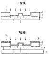
- FIGS 2a to 2d show a schematic representation a second embodiment of the method according to the invention.
- Fig. 2a shows a semiconductor structure, as for the Generation of CMOS circuits is used.
- a silicon wafer 1 On a silicon wafer 1 are n- and p-type silicon regions 2, a gate 3 and an STI insulation 4 are provided.
- a titanium silicide layer in the later contact hole areas is first by wet chemical cleaning (for example in buffered hydrofluoric acid) the natural oxide layer removed on the silicon.
- the silicon wafer 1 then under vacuum conditions baked at about 350 ° C.
- a titanium layer 7 is now sputtered.
- the fat the titanium layer 7 produced should be the desired one Titanium silicide layer thickness can be adjusted.
- the silicon wafer is transported into a cooling chamber under vacuum conditions.
- the disk which is still hot from sputtering, is placed there on a water-cooled chuck 8 and cooled to room temperature.
- the cooling is achieved by a thermal contact to the chuck 8, the thermal radiation of the silicon wafer and the interaction with the nitrogen-containing gas present in the cooling chamber, for example N 2 or NH 3 .
- nitrogen at 10 Torr for example, the cooling time can be shortened by around 40%.
- the titanium reacts with the nitrogen and a thin titanium nitride layer 9 is formed. The resulting situation is shown in Fig. 2b.
- the cooled disc is now removed from the sputtering system and for salting in an oven with a nitrogen and given hydrogen-containing atmosphere.
- the titanium reacts at the contact surface of titanium to silicon to titanium silicide 10.
- the titanium nitride layer 9 reinforced, so that usually no pure titanium is left behind. The resulting situation is shown in Fig. 2c.
- the titanium nitride becomes wet chemical for example with an ammonia and hydrogen peroxide Acid removed, so that on the silicon surfaces titanium silicide 10 remains.
Landscapes
- Chemical & Material Sciences (AREA)
- Chemical Kinetics & Catalysis (AREA)
- Engineering & Computer Science (AREA)
- Materials Engineering (AREA)
- Mechanical Engineering (AREA)
- Metallurgy (AREA)
- Organic Chemistry (AREA)
- Internal Circuitry In Semiconductor Integrated Circuit Devices (AREA)
- Electrodes Of Semiconductors (AREA)
- Solid-Phase Diffusion Into Metallic Material Surfaces (AREA)
- Physical Vapour Deposition (AREA)
Abstract

Description
Claims (10)
- Verfahren zur Erzeugung metallhaltiger Schichten, insbesondere metallhaltiger Diffusionsbarrieren, Kontaktschichten und/oder Antireflexschichten, auf einer Halbleiterstruktur mit den Schritten:a) Aufbringen einer Metallschicht mit einer vorgegebenen Dicke bei erhöhter Temperatur;b) Abkühlen der Metallschicht in einer stickstoffhaltigen Atmosphäre, so daß eine Metallnitridschicht gebildet wird.
- Verfahren nach Anspruch 1, dadurch gekennzeichnet, daß die Metallschicht bei einer Temperatur von mehr als 100°C, insbesondere mehr als 300°C, aufgebracht wird.
- Verfahren nach Anspruch 1 oder 2, dadurch gekennzeichnet, daß die Metallschicht auf eine Temperatur von weniger als 100°C abgekühlt wird.
- Verfahren nach einem der vorstehenden Ansprüche, dadurch gekennzeichnet, daß die Metallschicht durch ein CVD-Verfahren oder ein PVD-Verfahren, insbesondere eine Sputtertechnik, aufgebracht wird.
- Verfahren nach einem der vorstehenden Ansprüche, dadurch gekennzeichnet, daß als Metall Titan, Tantal, Molybdän oder Wolfram verwendet wird.
- Verfahren nach einem der vorstehenden Ansprüche, dadurch gekennzeichnet, daß eine Titanschicht auf eine Siliziumoberfläche aufgebracht wird.
- Verfahren nach Anspruch 6, dadurch gekennzeichnet, daß die Titanschicht nach dem Abkühlen in einer stickstoff- und wasserstoffhaltigen Atmosphäre einer Wärmebehandlung unterzogen wird, so daß das Titan an der Kontaktfläche zum Silizium zu Titansilizid reagiert.
- Verfahren nach Anspruch 7, dadurch gekennzeichnet, daß die Wärmebehandlung bei einer Temperatur von etwa 500 bis 1000°C, bevorzugt 600 bis 900°C, durchgeführt wird.
- Verfahren nach einem der vorstehenden Ansprüche, dadurch gekennzeichnet, daß die Metallnitridschicht, bevorzugt naßchemisch, entfernt wird.
- Verfahren nach einem der vorstehenden Ansprüche, dadurch gekennzeichnet, daß das Aufbringen der Metallschicht in einer ersten Kammer und das Abkühlen der Metallschicht in einer zweiten Kammer durchgeführt wird, wobei die Halbleiterstruktur nach dem Aufbringen der Metallschicht unter Beibehaltung der Vakuumbedindungen von der ersten Kammer in die zweite Kammer transportiert wird.
Applications Claiming Priority (2)
| Application Number | Priority Date | Filing Date | Title |
|---|---|---|---|
| DE19822749 | 1998-05-20 | ||
| DE19822749A DE19822749A1 (de) | 1998-05-20 | 1998-05-20 | Verfahren zur Erzeugung metallhaltiger Schichten |
Publications (3)
| Publication Number | Publication Date |
|---|---|
| EP0965654A2 true EP0965654A2 (de) | 1999-12-22 |
| EP0965654A3 EP0965654A3 (de) | 2002-10-09 |
| EP0965654B1 EP0965654B1 (de) | 2003-11-19 |
Family
ID=7868486
Family Applications (1)
| Application Number | Title | Priority Date | Filing Date |
|---|---|---|---|
| EP99109894A Expired - Lifetime EP0965654B1 (de) | 1998-05-20 | 1999-05-19 | Verfahren zur Erzeugung metallhaltiger Schichten |
Country Status (4)
| Country | Link |
|---|---|
| US (1) | US6403473B1 (de) |
| EP (1) | EP0965654B1 (de) |
| DE (2) | DE19822749A1 (de) |
| TW (1) | TW457516B (de) |
Cited By (1)
| Publication number | Priority date | Publication date | Assignee | Title |
|---|---|---|---|---|
| WO2002073689A3 (en) * | 2001-03-13 | 2003-04-10 | Applied Materials Inc | Integrated barrier layer structure for copper contact level metallization |
Families Citing this family (5)
| Publication number | Priority date | Publication date | Assignee | Title |
|---|---|---|---|---|
| DE19822749A1 (de) * | 1998-05-20 | 1999-12-02 | Siemens Ag | Verfahren zur Erzeugung metallhaltiger Schichten |
| NL1017748C2 (nl) * | 2001-03-30 | 2002-10-01 | Otb Group Bv | Werkwijze en inrichting voor het aanbrengen van lagen op een schijfvormige informatiedrager. |
| US8088196B2 (en) * | 2007-01-23 | 2012-01-03 | Air Products And Chemicals, Inc. | Purification of carbon dioxide |
| JP6823533B2 (ja) * | 2017-04-24 | 2021-02-03 | 東京エレクトロン株式会社 | チタンシリサイド領域を形成する方法 |
| CN113130636B (zh) | 2021-04-15 | 2022-06-17 | 长鑫存储技术有限公司 | 半导体器件的制造方法及其半导体器件 |
Family Cites Families (13)
| Publication number | Priority date | Publication date | Assignee | Title |
|---|---|---|---|---|
| US3655544A (en) * | 1970-03-02 | 1972-04-11 | Gen Electric | Refractory metal/refractory metal nitride resistor films |
| US5213848A (en) * | 1990-02-06 | 1993-05-25 | Air Products And Chemicals, Inc. | Method of producing titanium nitride coatings by electric arc thermal spray |
| US5021353A (en) * | 1990-02-26 | 1991-06-04 | Micron Technology, Inc. | Split-polysilicon CMOS process incorporating self-aligned silicidation of conductive regions |
| JPH0442412A (ja) * | 1990-06-08 | 1992-02-13 | Nissin Electric Co Ltd | 磁気ヘッド |
| JP2757927B2 (ja) * | 1990-06-28 | 1998-05-25 | インターナショナル・ビジネス・マシーンズ・コーポレイション | 半導体基板上の隔置されたシリコン領域の相互接続方法 |
| JPH05160070A (ja) * | 1991-05-31 | 1993-06-25 | Texas Instr Inc <Ti> | 半導体装置の接点とその製法 |
| US5811182A (en) * | 1991-10-04 | 1998-09-22 | Tulip Memory Systems, Inc. | Magnetic recording medium having a substrate and a titanium nitride underlayer |
| US5378660A (en) * | 1993-02-12 | 1995-01-03 | Applied Materials, Inc. | Barrier layers and aluminum contacts |
| US5401677A (en) * | 1993-12-23 | 1995-03-28 | International Business Machines Corporation | Method of metal silicide formation in integrated circuit devices |
| WO1995034092A1 (en) * | 1994-06-03 | 1995-12-14 | Materials Research Corporation | A method of nitridization of titanium thin films |
| US5610099A (en) * | 1994-06-28 | 1997-03-11 | Ramtron International Corporation | Process for fabricating transistors using composite nitride structure |
| US5990005A (en) * | 1997-02-10 | 1999-11-23 | Nec Corporation | Method of burying a contact hole with a metal for forming multilevel interconnections |
| DE19822749A1 (de) * | 1998-05-20 | 1999-12-02 | Siemens Ag | Verfahren zur Erzeugung metallhaltiger Schichten |
-
1998
- 1998-05-20 DE DE19822749A patent/DE19822749A1/de not_active Withdrawn
-
1999
- 1999-05-18 TW TW088108116A patent/TW457516B/zh not_active IP Right Cessation
- 1999-05-19 EP EP99109894A patent/EP0965654B1/de not_active Expired - Lifetime
- 1999-05-19 DE DE59907769T patent/DE59907769D1/de not_active Expired - Lifetime
- 1999-05-20 US US09/315,329 patent/US6403473B1/en not_active Expired - Lifetime
Cited By (1)
| Publication number | Priority date | Publication date | Assignee | Title |
|---|---|---|---|---|
| WO2002073689A3 (en) * | 2001-03-13 | 2003-04-10 | Applied Materials Inc | Integrated barrier layer structure for copper contact level metallization |
Also Published As
| Publication number | Publication date |
|---|---|
| US6403473B1 (en) | 2002-06-11 |
| TW457516B (en) | 2001-10-01 |
| EP0965654B1 (de) | 2003-11-19 |
| DE59907769D1 (de) | 2003-12-24 |
| DE19822749A1 (de) | 1999-12-02 |
| EP0965654A3 (de) | 2002-10-09 |
Similar Documents
| Publication | Publication Date | Title |
|---|---|---|
| DE69724317T2 (de) | Herstellungsverfahren für eine Vorrichtung bei dem eine dünne Kobaltsilizidschicht geformt wird | |
| US5665646A (en) | Method for manufacturing semiconductor device with low electric resistance silicide layer on silicon surface | |
| DE19950708C2 (de) | Verfahren zum Bilden von selbstjustierenden Cobaltsilicid-Schichten mit lokal unterschiedlicher Schichtdicke | |
| DE69030229T2 (de) | Verfahren zum Herstellen einer Halbleitervorrichtung | |
| DE69229983T2 (de) | Halbleiterschaltung mit einem Kontakt mit niedrigem Widerstand und ihr Herstellungsverfahren | |
| DE69427959T2 (de) | Integrierte Schaltung mit verbesserter Kontaktbarriere | |
| DE102006040764B4 (de) | Halbleiterbauelement mit einem lokal vorgesehenem Metallsilizidgebiet in Kontaktbereichen und Herstellung desselben | |
| EP0501561A1 (de) | Verfahren zum Herstellen einer Halbleiteranordnung, wobei ein selbstregistrierendes Kobalt- oder Nickelsilizid gebildet wird | |
| US20010008293A1 (en) | MIS transistor and manufacturing method thereof | |
| EP1152459A2 (de) | Verfahren zum Herstellen einer Barriereschicht in einem elektronischen Bauelement | |
| DE19521150A1 (de) | Verdrahtungsstruktur eines Halbleiterbaulementes und Verfahren zu ihrer Herstellung | |
| DE19505947A1 (de) | Halbleitervorrichtung | |
| JP2677168B2 (ja) | 半導体装置の製造方法 | |
| JPH09153616A (ja) | 半導体装置およびその製造方法 | |
| DE4423558B4 (de) | Halbleiterbauelement mit einer leitfähigen Schicht, MOS-Feldeffekttransistor mit einer leitfähigen Schicht und Verfahren zu deren Herstellung | |
| KR20050052926A (ko) | 열적 안정성이 우수한 실리사이드막 형성방법, 이방법으로 형성된 실리사이드막이 구비된 반도체 소자와반도체 메모리 소자 및 이들 소자의 제조 방법 | |
| DE10345374B4 (de) | Halbleiterbauteil mit einem Nickel/Kobaltsilizidgebiet, das in einem Siliziumgebiet gebildet ist und Verfahren zu seiner Herstellung | |
| DE19741891A1 (de) | Verfahren zur gleichzeitigen Bildung von Metallsalicid und einer lokalen Verbindungsstruktur in einer IC-Struktur | |
| DE10056866C2 (de) | Verfahren zur Bildung einer Ätzstoppschicht während der Herstellung eines Halbleiterbauteils | |
| DE69931656T2 (de) | VERFAHREN ZUR HERSTELLUNG EINER SiON/SiO2 DIELEKTRISCHEN ZWISCHENSCHICHT MIT EINER NACHBEHANDLUNG DER CVD SILIZIUM OXYNITRIDSCHICHT | |
| KR20040034394A (ko) | 양질의 코발트 실리사이드막 형성을 위한 개선된 코발트실리사이드 형성 방법 및 이를 이용한 반도체 소자의 제조방법 | |
| EP0965654B1 (de) | Verfahren zur Erzeugung metallhaltiger Schichten | |
| JPH0661177A (ja) | 半導体集積回路装置およびその製造方法 | |
| US6653227B1 (en) | Method of cobalt silicidation using an oxide-Titanium interlayer | |
| US5166095A (en) | Low contact resistance process |
Legal Events
| Date | Code | Title | Description |
|---|---|---|---|
| PUAI | Public reference made under article 153(3) epc to a published international application that has entered the european phase |
Free format text: ORIGINAL CODE: 0009012 |
|
| AK | Designated contracting states |
Kind code of ref document: A2 Designated state(s): AT BE CH CY DE DK ES FI FR GB GR IE IT LI LU MC NL PT SE |
|
| AX | Request for extension of the european patent |
Free format text: AL;LT;LV;MK;RO;SI |
|
| RTI1 | Title (correction) |
Free format text: PROCESS FOR MANUFACTURING METAL-CONTAINING LAYERS |
|
| RAP1 | Party data changed (applicant data changed or rights of an application transferred) |
Owner name: INFINEON TECHNOLOGIES AG |
|
| PUAL | Search report despatched |
Free format text: ORIGINAL CODE: 0009013 |
|
| RIC1 | Information provided on ipc code assigned before grant |
Free format text: 7C 23C 16/06 A, 7C 23C 16/56 B, 7C 23C 14/16 B, 7C 23C 14/58 B, 7H 01L 21/285 B, 7H 01L 21/768 B |
|
| AK | Designated contracting states |
Kind code of ref document: A3 Designated state(s): AT BE CH CY DE DK ES FI FR GB GR IE IT LI LU MC NL PT SE |
|
| AX | Request for extension of the european patent |
Free format text: AL;LT;LV;MK;RO;SI |
|
| 17P | Request for examination filed |
Effective date: 20021031 |
|
| GRAH | Despatch of communication of intention to grant a patent |
Free format text: ORIGINAL CODE: EPIDOS IGRA |
|
| AKX | Designation fees paid |
Designated state(s): DE FR GB IE IT |
|
| GRAS | Grant fee paid |
Free format text: ORIGINAL CODE: EPIDOSNIGR3 |
|
| GRAA | (expected) grant |
Free format text: ORIGINAL CODE: 0009210 |
|
| AK | Designated contracting states |
Kind code of ref document: B1 Designated state(s): DE FR GB IE IT |
|
| REG | Reference to a national code |
Ref country code: GB Ref legal event code: FG4D Free format text: NOT ENGLISH |
|
| REF | Corresponds to: |
Ref document number: 59907769 Country of ref document: DE Date of ref document: 20031224 Kind code of ref document: P |
|
| REG | Reference to a national code |
Ref country code: IE Ref legal event code: FG4D Free format text: GERMAN |
|
| GBT | Gb: translation of ep patent filed (gb section 77(6)(a)/1977) |
Effective date: 20040209 |
|
| ET | Fr: translation filed | ||
| PLBE | No opposition filed within time limit |
Free format text: ORIGINAL CODE: 0009261 |
|
| STAA | Information on the status of an ep patent application or granted ep patent |
Free format text: STATUS: NO OPPOSITION FILED WITHIN TIME LIMIT |
|
| 26N | No opposition filed |
Effective date: 20040820 |
|
| REG | Reference to a national code |
Ref country code: GB Ref legal event code: 732E Free format text: REGISTERED BETWEEN 20100916 AND 20100922 |
|
| REG | Reference to a national code |
Ref country code: GB Ref legal event code: 732E Free format text: REGISTERED BETWEEN 20110804 AND 20110810 |
|
| REG | Reference to a national code |
Ref country code: FR Ref legal event code: TP Owner name: QIMONDA AG,, DE Effective date: 20120123 |
|
| REG | Reference to a national code |
Ref country code: FR Ref legal event code: PLFP Year of fee payment: 17 |
|
| REG | Reference to a national code |
Ref country code: DE Ref legal event code: R081 Ref document number: 59907769 Country of ref document: DE Owner name: POLARIS INNOVATIONS LTD., IE Free format text: FORMER OWNER: QIMONDA AG, 81739 MUENCHEN, DE Ref country code: DE Ref legal event code: R081 Ref document number: 59907769 Country of ref document: DE Owner name: INFINEON TECHNOLOGIES AG, DE Free format text: FORMER OWNER: QIMONDA AG, 81739 MUENCHEN, DE |
|
| REG | Reference to a national code |
Ref country code: DE Ref legal event code: R081 Ref document number: 59907769 Country of ref document: DE Owner name: POLARIS INNOVATIONS LTD., IE Free format text: FORMER OWNER: INFINEON TECHNOLOGIES AG, 85579 NEUBIBERG, DE |
|
| REG | Reference to a national code |
Ref country code: GB Ref legal event code: 732E Free format text: REGISTERED BETWEEN 20151015 AND 20151021 |
|
| REG | Reference to a national code |
Ref country code: FR Ref legal event code: TP Owner name: INFINEON TECHNOLOGIES AG, DE Effective date: 20160212 |
|
| REG | Reference to a national code |
Ref country code: FR Ref legal event code: PLFP Year of fee payment: 18 |
|
| PGFP | Annual fee paid to national office [announced via postgrant information from national office to epo] |
Ref country code: GB Payment date: 20160518 Year of fee payment: 18 Ref country code: IE Payment date: 20160509 Year of fee payment: 18 |
|
| PGFP | Annual fee paid to national office [announced via postgrant information from national office to epo] |
Ref country code: IT Payment date: 20160524 Year of fee payment: 18 Ref country code: FR Payment date: 20160412 Year of fee payment: 18 |
|
| GBPC | Gb: european patent ceased through non-payment of renewal fee |
Effective date: 20170519 |
|
| REG | Reference to a national code |
Ref country code: IE Ref legal event code: MM4A |
|
| REG | Reference to a national code |
Ref country code: FR Ref legal event code: ST Effective date: 20180131 |
|
| PG25 | Lapsed in a contracting state [announced via postgrant information from national office to epo] |
Ref country code: GB Free format text: LAPSE BECAUSE OF NON-PAYMENT OF DUE FEES Effective date: 20170519 Ref country code: IE Free format text: LAPSE BECAUSE OF NON-PAYMENT OF DUE FEES Effective date: 20170519 |
|
| PG25 | Lapsed in a contracting state [announced via postgrant information from national office to epo] |
Ref country code: FR Free format text: LAPSE BECAUSE OF NON-PAYMENT OF DUE FEES Effective date: 20170531 Ref country code: IT Free format text: LAPSE BECAUSE OF NON-PAYMENT OF DUE FEES Effective date: 20170519 |
|
| PGFP | Annual fee paid to national office [announced via postgrant information from national office to epo] |
Ref country code: DE Payment date: 20180508 Year of fee payment: 20 |
|
| REG | Reference to a national code |
Ref country code: DE Ref legal event code: R071 Ref document number: 59907769 Country of ref document: DE |