EP0965060B1 - Dispositif optique a selection de la longueur d'onde et ayant au moins une structure reseau de bragg - Google Patents
Dispositif optique a selection de la longueur d'onde et ayant au moins une structure reseau de bragg Download PDFInfo
- Publication number
- EP0965060B1 EP0965060B1 EP98908412A EP98908412A EP0965060B1 EP 0965060 B1 EP0965060 B1 EP 0965060B1 EP 98908412 A EP98908412 A EP 98908412A EP 98908412 A EP98908412 A EP 98908412A EP 0965060 B1 EP0965060 B1 EP 0965060B1
- Authority
- EP
- European Patent Office
- Prior art keywords
- waveguide
- mmi
- access
- waveguides
- bragg
- Prior art date
- Legal status (The legal status is an assumption and is not a legal conclusion. Google has not performed a legal analysis and makes no representation as to the accuracy of the status listed.)
- Expired - Lifetime
Links
Images

Classifications
-
- G—PHYSICS
- G02—OPTICS
- G02B—OPTICAL ELEMENTS, SYSTEMS OR APPARATUS
- G02B6/00—Light guides; Structural details of arrangements comprising light guides and other optical elements, e.g. couplings
- G02B6/10—Light guides; Structural details of arrangements comprising light guides and other optical elements, e.g. couplings of the optical waveguide type
- G02B6/12—Light guides; Structural details of arrangements comprising light guides and other optical elements, e.g. couplings of the optical waveguide type of the integrated circuit kind
- G02B6/12007—Light guides; Structural details of arrangements comprising light guides and other optical elements, e.g. couplings of the optical waveguide type of the integrated circuit kind forming wavelength selective elements, e.g. multiplexer, demultiplexer
-
- G—PHYSICS
- G02—OPTICS
- G02B—OPTICAL ELEMENTS, SYSTEMS OR APPARATUS
- G02B6/00—Light guides; Structural details of arrangements comprising light guides and other optical elements, e.g. couplings
- G02B6/10—Light guides; Structural details of arrangements comprising light guides and other optical elements, e.g. couplings of the optical waveguide type
- G02B6/12—Light guides; Structural details of arrangements comprising light guides and other optical elements, e.g. couplings of the optical waveguide type of the integrated circuit kind
- G02B2006/12083—Constructional arrangements
- G02B2006/12107—Grating
-
- G—PHYSICS
- G02—OPTICS
- G02B—OPTICAL ELEMENTS, SYSTEMS OR APPARATUS
- G02B6/00—Light guides; Structural details of arrangements comprising light guides and other optical elements, e.g. couplings
- G02B6/24—Coupling light guides
- G02B6/26—Optical coupling means
- G02B6/28—Optical coupling means having data bus means, i.e. plural waveguides interconnected and providing an inherently bidirectional system by mixing and splitting signals
- G02B6/2804—Optical coupling means having data bus means, i.e. plural waveguides interconnected and providing an inherently bidirectional system by mixing and splitting signals forming multipart couplers without wavelength selective elements, e.g. "T" couplers, star couplers
- G02B6/2808—Optical coupling means having data bus means, i.e. plural waveguides interconnected and providing an inherently bidirectional system by mixing and splitting signals forming multipart couplers without wavelength selective elements, e.g. "T" couplers, star couplers using a mixing element which evenly distributes an input signal over a number of outputs
- G02B6/2813—Optical coupling means having data bus means, i.e. plural waveguides interconnected and providing an inherently bidirectional system by mixing and splitting signals forming multipart couplers without wavelength selective elements, e.g. "T" couplers, star couplers using a mixing element which evenly distributes an input signal over a number of outputs based on multimode interference effect, i.e. self-imaging
Definitions
- the present invention relates to an optical wavelength selective device, and then particularly to a device for multiplexing/demultiplexing optical transmission channels in an optical network, such as an add/drop multiplexor.
- WDM wavelength division multiplexing
- One type of multiplexing of particular interest with regard to so-called bus networks or ring networks is add/drop multiplexing, i.e. a process in which one or more so-called information channels disposed on the aforesaid carrier wavelengths are dropped from or added to an information flow.
- transmission channels are multiplexed and demultiplexed on different carrier wavelengths to obtain an information flow.
- Another problem is one of maintaining an acceptable channel cross-talk level.
- the present invention attacks these problems with the aid of an optical device that includes at least one MMI-structure, at least one Bragg-grating, and at least two so-called access waveguides for connection to external optical devices or optical fibres.
- the aforesaid MMI-structure has the ability of enabling light intensity distribution at one of the inputs of the MMI-structure to be imaged on all outputs of said MMI-structure.
- MMI-structures can therefore be used to split light.
- the length of the MMI waveguide is chosen to obtain 1:1 imaging, in other words in the optimal case all light incoming from a first access waveguide provided on the MMI waveguide is focused out on a second access waveguide disposed on the opposite side relative to the first access waveguide.
- a more fundamental theory behind MMI-structures is treated in Patent Specification DE 2506272 and in L.B. Soldano and E.C.M. Pennings, "Optical Multi-Mode Interference Devices Based on Self-Imaging: Principles and Application", J. Lightwave Technol., Vol. 13(4), pp. 615-627, 1995 .
- Bragg-grating is used to filter light. This filtering process involves permitting light of certain wavelengths to pass through the grating while reflecting light of other wavelengths.
- a Bragg-grating can be said to constitute some form of wavelength selective mirror. Reflection of certain wavelengths can be achieved in several different ways. However, it is typical of such methods that reflection takes place by changing a so-called material index periodically in the waveguide.
- the inventive device may also include a so-called phase control element.
- the phase control element influences a so-called optical wavelength in a waveguide. This is effected by applying an external signal to the waveguide.
- One method of achieving said phase control is to subject the waveguide to an electric field that changes the effective refraction index in the waveguide.
- the phase control can also be achieved by subjecting the waveguide to thermal changes.
- One method of permanently changing the index in a waveguide is to expose the waveguide to ultraviolet light. This is normally referred to as the waveguide being UV-written.
- the technique is most often used to achieve periodic refractive index variation, so-called UV-writing.
- the technique can also be used for adjusting or trimming purposes.
- the invention includes an MMI-structure in which a Bragg-grating is arranged.
- the Bragg-grating is preferably arranged in the centre of the MMI-structure.
- Access waveguides are provided on the MMI-structure. The placement of these access waveguides on the MMI-structure is decisive to the function of the optical device.
- the invention solves the aforesaid problem, by virtue of a number of different embodiments of the MMI-structure on the one hand and of the access waveguides together with the Bragg-grating on the other.
- the object of the present invention is thus to provide an optical device that has smaller power losses, less channel cross-talk and smaller power variations between different transmission channels in comparison with known technology.
- One advantage afforded by the present invention is that the device is more compact that known devices.
- Another advantage is that the inventive optical device can be produced relatively cheaply.
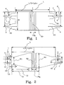
- FIG 1 illustrates an embodiment of an inventive optical wavelength selective device.
- the optical wavelength selective device includes a Bragg-grating 50 and an MMI-waveguide.
- the Bragg-grating 50 may be arranged in the MMI-waveguide so that its centre line coincides with the centre line of the MMI-waveguide.
- the Bragg-grating may also be arranged at a distance of L/2+Lphc from one short side of the MMI-waveguide, where Lphc indicates said displacement from the centre of the MMI-waveguide. Lphc may either be positive or negative.
- the Bragg-grating is offset from the centre of the MMI-waveguide so as to compensate out the mode-dependent phase shift that would otherwise threaten the function of the device.
- the Bragg-grating has a given width, referenced LBg.
- the MMI-waveguide has a given length, which is referenced L in Figure 1.
- So-called access waveguides 1, 2, 3, 4 may be provided on the short sides of the MMI-waveguide.
- the Figure 1 embodiment includes four access waveguides, i.e. two access waveguides on each short side.
- the number of access waveguides may vary from one embodiment to another, depending on the intended use of the optical wavelength selective device.
- the centre lines 10, 20, 30 and 40 of the access waveguides have been shown in the Figure.
- the distance from one long side of the MMI-waveguide to the centre line 10 of the access waveguide 1 is referenced a in Figure 1.
- the distance from the same said long side of the MMI-waveguide to the centre line 20 of the access waveguide 2 is referenced b in Figure 1.
- the distance from said long side of the MMI-waveguide to remaining access waveguides 3 and 4 is referenced c and d respectively.
- the distances a and c may be equal and the distances b and d may also be equal.
- the distances a, b, c and d will depend on the effective width We of the MMI-waveguide, the number of images and the type of MMI-waveguide concerned.
- a profound theory behind different MMI-waveguides is treated in an article by Pierre A. Besse et al, entitled Optical Bandwidth and Fabrication Tolerances of Multimode Interference Couplers, J. Lightwave Technology, Vol. 12(4), pp. 1004-1009, 1994 .
- the effective width We of the MMI-waveguide depends on the wavelength X, the refractive index step in the MMI-waveguide, the physical width of the MMI-waveguide and the polarization of the light.
- the length of the MMI-waveguide will depend on the effective width We of said waveguide and the desired power.
- the access waveguides are broader at their connections to the MMI-waveguide than at their free ends.
- This structure is normally referred to as a tapered structure.
- the effect of this structure is to change the optical field in comparison with a straight access waveguide. This results in a larger error tolerance with respect to error correction of the access waveguides.
- the effect will lie to a great extent in the lower order modes, which is beneficial because the Bragg-grating will give a mode-dependent phase shift for reflected channels.
- the illustrated optical wavelength selective device may also include a phase control element.
- This phase control element may be arranged in any one of a number of different ways. A number of conceivable ways of arranging the phase control element have been dealt with under the heading Summary of the Invention and are known to one of normal skill in this field and will not therefore be described in more detail in this document.
- Figure 2 illustrates another embodiment of the inventive optical wavelength selective device.
- the Figure 2 embodiment includes a Bragg-grating 50 and an MMI-waveguide.
- the width of the Bragg-grating is referenced LBg.
- the length of the MMI-waveguide is referenced L, as in the case of the aforedescribed embodiment.
- the difference between this embodiment and the first embodiment resides in the form of the MMI-waveguide.
- the waveguide is tapered, similar to the access waveguides 1, 2, 3 and 4.
- the long sides of the MMI-waveguide are mutually parallel for a short distance on both sides around the Bragg-grating in the longitudinal direction of the MMI-waveguide and orthogonal to an imaginary centre line in the longitudinal direction of the MMI-waveguide.
- the width of the MMI-waveguide immediately adjacent the Bragg-grating is referenced W2.
- the width of the short sides of the MMI-waveguide is referenced W1, where W1 ⁇ W2.
- the MMI-waveguide may include a final part having a length L3.
- the length L3 may be equal to zero.
- the structure is tapered between the width W1 and W2 of the MMI-waveguide.
- the taper structure may be linear, parabolic or some other shape.
- the object of the taper structure is to reduce the difference between the propagation modes and therewith reduce the difference in the so-called effective penetration depth of the reflected modes in the grating.
- Access waveguides 1, 2, 3 and 4 are arranged on the short sides of the MMI-waveguide.
- two such access waveguides are arranged on each short side.
- the centre lines 10, 20, 30 and 40 of respective access waveguides 1, 2, 3 and 4 have been shown in the Figure, as in the illustration of the former embodiment.
- the distance from one end of the short side to the centre line 10 of the access waveguide 1 is referenced a.
- the distance from the same one end of the short side to the centre line 20 of the access waveguide 2 is referenced b.
- the distances of the remaining access waveguides from the other short side are referenced c and d.
- the distances a and c may be equal, and the distances b and d may also be equal.
- the Bragg-grating may either be arranged in the centre of the MMI-waveguide or may be offset slightly from said centre.
- the Bragg-grating is offset from the centre of the waveguide for precisely the same reason as that mentioned with reference to the former embodiment, in other words in order to compensate out any mode-dependent phase shift.
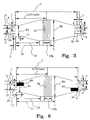
- Figure 3 illustrates another embodiment of an inventive optical wavelength selective device.
- the optical so-called pathlength has been in respect of a number of access waveguides.
- the optical pathlength has been extended for access waveguides 2 and 3, by arranging the waveguides on an outwardly projecting part of the MMI-waveguide.
- the width of these outwardly projecting parts has been referenced e and f respectively in Figure 3.
- the distances e and f may be equal or different, depending on the desired result. It is, of course, possible to arrange any of the access waveguides, one or more of said waveguides, on some form of means on the MMI-waveguide that will change the optical pathlength.
- cross-mode a mode in which at least one wavelength channel incoming from one side of the MMI-waveguide is transmitted through the MMI-waveguide so as to be focused on an access waveguide on the other side of the MMI-waveguide that is offset laterally in relation to the access waveguide - from which the signal exited.
- An example of a cross-mode is when a wavelength channel is transmitted from access waveguide 10 and focused on access waveguide 40.
- bar-mode is meant that a wavelength channel is transmitted from one access waveguide on one side of the MMI-waveguide and focused on a corresponding access waveguide disposed on the other side of said MMI-waveguide.
- An example of a bar-mode is when a wavelength channel is transmitted from access waveguide 10 and focused on access waveguide 30.
- FIG 4 illustrates a further embodiment of an inventive optical wavelength selective device.
- two MMI-waveguides are arranged one after the other.
- the MMI-waveguides have been joined together either by a waveguide or by an optical fibre.
- the structure of respective MMI-waveguides is essentially similar to the structure shown in Figure 2, except at the ends at which they are joined together. It will be seen from Figure 4 that these ends include only one access waveguide. Furthermore, a part p , q of respective short sides does not lie orthogonal to the centre line of the access waveguide. The reason for this is to enable undesirable light in the MMI-waveguide to be refracted at this part of the structure and disappear therefrom.
- a cascade of two sequentially arranged MMI-waveguides has the effect of reducing cross-talk. It is also feasible to include in this embodiment a phase control element of the kind mentioned in the Summary of the Invention. Any required number of access waveguides may be arranged on the two MMI-waveguides, although the access waveguides will preferably be two in number on one side and two in number on the other, opposite side. As evident from the Figure, the Bragg-grating may be offset from the centre of the MMI-waveguide, or may be arranged in the centre of said waveguide.
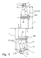
- FIG. 5 illustrates another embodiment of an inventive optical wavelength selective device in which two MMI-waveguides have been directly combined.
- the MMI-waveguide of this embodiment is tapered solely on the side on which the access waveguides are arranged.
- the respective long sides of the MMI-waveguides are mutually parallel between the two Bragg-gratings.
- the centre line of one MMI-waveguide is laterally offset in parallel in relation to the centre line of the other MMI-waveguide.
- the parts p and q have been angled on respective MMI-waveguides, said parts being left over in the aforesaid lateral parallel displacement of said centre line so to speak.
- This embodiment may also include a phase control element of the kind mentioned under the heading Summary of the Invention. Any desired number of access waveguides may be arranged in the free ends of respective MMI-waveguides, a practical limit with respect to this number being determined by the dimensions of the MMI-waveguides.
- the refractive index of the MMI-waveguide can be changed in connection with? suitable access waveguides while achieving the same effect, that is to say change the optical pathlength within the MMI-waveguide with the purpose of compensating for mode-dependent phase shifts.
- This alternative is illustrated in Figure 6.
- the refractive index of the MMI-waveguide has been increased in a rectangular area 60, immediately adjacent a pair of access waveguides with the longitudinal centre line of the rectangle coinciding with the centre lines of respective access waveguides.
- This change in refractive index can be achieved by transforming existing material in the MMI-waveguide by UV writing, for instance.
- the form and dimensions of said refractive index change are decisive in achieving this effect.
- the inventive device may suitably be produced from such materials as quartz (SiO 2 ), polymeric materials, some semiconductor system, or lithiumniobate (LiNbO 3 ), although preferably quartz is used.
Claims (14)
- Moyen multiplexeur d'extraction/addition optique qui comprend au moins un guide d'ondes MMI et au moins deux guides d'ondes dits d'accès (1, 2) implantés sur un premier côté du guide d'ondes MMI et au moins un guide d'ondes d'accès (3, 4) implanté sur un second côté du guide d'ondes MMI, lesdits premier et second côtés étant les petits côtés dudit guide d'ondes MMI, dans lequel lesdits petits côtés sont plus courts qu'au moins un autre côté du guide d'ondes MMI ; caractérisé en ce que lesdits guides d'ondes d'accès (1, 2, 3, 4) ont une structure dite conique, si bien que lesdits guides d'ondes d'accès (1, 2, 3, 4) sont plus larges au niveau de leurs connexions avec le guide d'ondes MMI qu'à leurs extrémités libres ; et en ce qu'au moins une structure à réseau de Bragg (50) est implantée dans le guide d'ondes MMI.
- Moyen multiplexeur d'extraction/addition optique selon la revendication 1, caractérisé en ce que la structure à réseau de Bragg (50) est implantée au centre du guide d'ondes MMI.
- Moyen multiplexeur d'extraction/addition optique selon la revendication 1, caractérisé en ce que la structure à réseau de Bragg (50) est décalée par rapport à l'axe central du guide d'ondes MMI, ledit axe central étant perpendiculaire à la direction de propagation de lumière dans le guide d'ondes MMI.
- Moyen multiplexeur d'extraction/addition optique selon la revendication 2 ou 3, caractérisé en ce que le dispositif comprend un élément de commande de phase activé thermiquement, optiquement ou électriquement.
- Moyen multiplexeur d'extraction/addition optique selon la revendication 4, caractérisé en ce que le guide d'ondes MMI a une structure conique de chaque côté de la structure à réseau de Bragg (50), si bien que ledit guide d'ondes MMI est plus large au niveau de sa connexion avec la structure à réseau de Bragg qu'à son autre extrémité.
- Moyen multiplexeur d'extraction/addition optique selon la revendication 5, caractérisé en ce que la structure conique du guide d'ondes MMI est linéaire.
- Moyen multiplexeur d'extraction/addition optique selon la revendication 5, caractérisé en ce que la structure conique du guide d'ondes MMI est parabolique.
- Moyen multiplexeur d'extraction/addition optique selon la revendication 6 ou 7, caractérisé en ce qu'au moins un guide d'ondes d'accès (1) est implanté de telle manière sur ledit un côté du guide d'ondes MMI que la longueur de trajet optique de ce guide d'ondes d'accès diffère des longueurs de trajet optique des guides d'ondes d'accès restants (2, 3, 4).
- Moyen multiplexeur d'extraction/addition optique selon la revendication 6 ou 7, caractérisé en ce qu'il possède au moins trois guides d'ondes d'accès (1, 2, 3, 4), et en ce qu'au moins un guide d'ondes d'accès (1, 3) est implanté sur le premier et le second côté du guide d'ondes MMI de manière à ce que les longueurs de trajet optique dudit au moins un guide d'ondes d'accès implanté sur le premier et sur le second côté du guide d'ondes MMI diffèrent des longueurs de trajet optique des guides d'ondes d'accès restants (2, 4).
- Moyen multiplexeur d'extraction/addition optique selon la revendication 8 ou 9, caractérisé en ce qu'un guide d'ondes d'accès sur un premier guide d'ondes MMI est couplé à un guide d'ondes d'accès sur un second guide d'ondes MMI.
- Moyen multiplexeur d'extraction/addition optique selon la revendication 1, caractérisé en ce qu'une partie (60) du guide d'ondes MMI, adjacente à au moins un guide d'ondes d'accès dans le guide d'ondes MMI, possède un indice de réfraction qui diffère de l'indice de réfraction des parties restantes du guide d'ondes MMI.
- Moyen multiplexeur d'extraction/addition optique selon la revendication 11, caractérisé en ce que le dispositif comprend au moins deux guides d'ondes MMI et au moins deux structures à réseau de Bragg (50), dans lequel au moins un guide d'ondes dit d'accès (1, 2) est implanté sur un premier côté d'un premier guide d'ondes MMI et au moins un guide d'ondes d'accès (3, 4) est implanté sur un second côté d'un second guide d'ondes MMI, et dans lequel lesdits premier et second côtés sont des petits côtés du guide d'ondes MMI, dans lequel lesdits petits côtés sont plus courts qu'au moins un autre côté du guide d'ondes MMI ; en ce qu'un second côté court du premier guide d'ondes MMI et un premier côté du second guide d'ondes MMI sont couplés ensemble ; en ce que lesdits guides d'ondes d'accès ont une structure dite conique si bien que lesdits guides d'ondes d'accès (1, 2, 3, 4) sont plus larges au niveau de leurs connexions avec le guide d'ondes MMI qu'à leurs extrémités libres ; et en ce que les structures à réseau de Bragg (50) sont implantées dans les guides d'ondes MMI.
- Moyen multiplexeur d'extraction/addition optique selon la revendication 12, caractérisé en ce que le second côté du premier guide d'ondes MMI et le premier côté du second guide d'ondes MMI sont décalés latéralement l'un par rapport à l'autre.
- Moyen multiplexeur d'extraction/addition optique selon la revendication 13, caractérisé en ce que les guides d'ondes MMI possèdent une structure conique de chaque côté des structures à réseau de Bragg (50), si bien que lesdits guides d'ondes MMI sont plus larges au niveau de leurs connexions à la structure à réseau de Bragg (50) qu'à leur autre extrémité.
Applications Claiming Priority (4)
| Application Number | Priority Date | Filing Date | Title |
|---|---|---|---|
| SE9700829 | 1997-03-07 | ||
| SE9700829A SE520432C2 (sv) | 1997-03-07 | 1997-03-07 | Optisk anordning för våglängdsmultiplexering/demultiplexering innefattande MMI-vågledare och Braggreflektorstruktur. |
| US09/033,092 US6047096A (en) | 1997-03-07 | 1998-03-02 | Optical device |
| PCT/SE1998/000393 WO1998039679A1 (fr) | 1997-03-07 | 1998-03-05 | Dispositif optique a selection de la longueur d'onde et ayant au moins une structure reseau de bragg |
Publications (2)
| Publication Number | Publication Date |
|---|---|
| EP0965060A1 EP0965060A1 (fr) | 1999-12-22 |
| EP0965060B1 true EP0965060B1 (fr) | 2008-01-09 |
Family
ID=26662925
Family Applications (1)
| Application Number | Title | Priority Date | Filing Date |
|---|---|---|---|
| EP98908412A Expired - Lifetime EP0965060B1 (fr) | 1997-03-07 | 1998-03-05 | Dispositif optique a selection de la longueur d'onde et ayant au moins une structure reseau de bragg |
Country Status (5)
| Country | Link |
|---|---|
| US (1) | US6047096A (fr) |
| EP (1) | EP0965060B1 (fr) |
| CN (1) | CN1120380C (fr) |
| AU (1) | AU6644598A (fr) |
| WO (1) | WO1998039679A1 (fr) |
Families Citing this family (28)
| Publication number | Priority date | Publication date | Assignee | Title |
|---|---|---|---|---|
| JP2000056153A (ja) * | 1998-08-12 | 2000-02-25 | Kdd Corp | 波長フィルタ |
| SE514820C2 (sv) | 1999-02-19 | 2001-04-30 | Ericsson Telefon Ab L M | Våglängdsselektiv modulator och förfarande för modulering av optiska våglängdskanaler |
| US6587615B1 (en) * | 1999-05-11 | 2003-07-01 | Jds Fitel Inc. | Wavelength multiplexer-demultiplexer having a wide flat response within the spectral passband |
| US6421478B1 (en) * | 1999-05-11 | 2002-07-16 | Jds Fitel Inc. | Tapered MMI coupler |
| US6317256B1 (en) * | 2000-02-15 | 2001-11-13 | Trw Inc. | Method of gain and noise figure equalization for simultaneous optical splitter/amplifier |
| US6571038B1 (en) * | 2000-03-01 | 2003-05-27 | Lucent Technologies Inc. | Multimode interference coupler with tunable power splitting ratios and method of tuning |
| GB2368131A (en) * | 2000-10-11 | 2002-04-24 | Marconi Caswell Ltd | Flared optical waveguide coupler |
| US6563988B2 (en) * | 2001-04-25 | 2003-05-13 | Lightwave Microsystems Corporation | Optical apparatus and method having predetermined group velocity dispersion |
| IL145320A (en) * | 2001-09-06 | 2006-12-10 | Gilad Optical Switches Ltd | Tunable optical filter |
| DE10145277B4 (de) * | 2001-09-14 | 2007-04-05 | Photeon Technologies Gmbh | Optischer Wellenleiter mit Taper und Wellenlängenmultiplexer/-demultiplexer mit einem solchen Wellenleiter oder solchen Wellenleitern |
| US6993224B1 (en) | 2001-11-15 | 2006-01-31 | UNIVERSITé LAVAL | Segmented waveguide array gratings (SWAG)-based archival optical memory |
| AU2002342458A1 (en) * | 2001-11-15 | 2003-05-26 | Universite Laval | Array grating filters as segmented waveguide |
| GB2384572A (en) * | 2002-01-25 | 2003-07-30 | Denselight Semiconductors Pte | Optical waveguide tap with multimode interferometer(MMI) |
| TW594090B (en) | 2003-05-20 | 2004-06-21 | Univ Nat Taiwan Normal | SOI integrated reconfigurable optical add/drop multiplexer and manufacturing method thereof |
| JP4534985B2 (ja) * | 2003-08-28 | 2010-09-01 | 日本電気株式会社 | 導波路型光デバイスおよびその製造方法 |
| CN100409049C (zh) * | 2004-05-28 | 2008-08-06 | 日立化成工业株式会社 | 包含光波导的光学系统 |
| JP4010012B2 (ja) | 2004-05-28 | 2007-11-21 | 日立化成工業株式会社 | 光導波路を含む光システム |
| JP5454256B2 (ja) * | 2010-03-17 | 2014-03-26 | 富士通株式会社 | 光導波路素子及びそのような光導波路素子を備えた光受信機 |
| GB2488308A (en) * | 2011-01-19 | 2012-08-29 | Univ Surrey | Optical Filter |
| US20150086158A1 (en) * | 2013-09-26 | 2015-03-26 | Mitsubishi Electric Corporation | Multi-Mode Phase-Shifting Interference Device |
| JP6711025B2 (ja) * | 2016-03-03 | 2020-06-17 | 株式会社豊田中央研究所 | グレーティングカプラ、グレーティングカプラアレイ、結像光学系、光スキャナ、及びレーザレーダ装置 |
| CN105572796B (zh) * | 2016-03-07 | 2018-08-21 | 龙岩学院 | 一种基于反对称多模布拉格波导光栅的上下路滤波器 |
| CN105759362A (zh) * | 2016-05-13 | 2016-07-13 | 龙岩学院 | 一种基于反对称多模布拉格波导光栅的带通带阻滤波器 |
| WO2018198193A1 (fr) * | 2017-04-25 | 2018-11-01 | 三菱電機株式会社 | Dispositif à semiconducteur et procédé de fabrication d'un dispositif à semiconducteur |
| CN107092056B (zh) * | 2017-06-12 | 2019-07-05 | 北京大学 | 一种波分复用/解复用器及其制作方法 |
| EP3629068A4 (fr) | 2017-06-16 | 2020-06-03 | Huawei Technologies Co., Ltd. | Multiplexeur d'insertion-extraction optique |
| CN110703385B (zh) * | 2019-11-11 | 2021-04-02 | 西湖大学 | 基于光散射的图案化的多模干涉耦合器、设计方法和应用 |
| US11609392B1 (en) * | 2022-02-24 | 2023-03-21 | X Development Llc | Photonic coupler |
Citations (3)
| Publication number | Priority date | Publication date | Assignee | Title |
|---|---|---|---|---|
| JPS6215879A (ja) * | 1985-07-12 | 1987-01-24 | Sharp Corp | 半導体レ−ザアレイ装置 |
| WO1996008044A2 (fr) * | 1994-09-06 | 1996-03-14 | Philips Electronics N.V. | Dispositif semi-conducteur optoelectronique dote d'un laser a diode a semi-conducteur |
| EP0826988A2 (fr) * | 1996-08-27 | 1998-03-04 | Lucent Technologies Inc. | Filtres d'encoche en optique intégrée planaire |
Family Cites Families (7)
| Publication number | Priority date | Publication date | Assignee | Title |
|---|---|---|---|---|
| DE2930681A1 (de) * | 1979-07-28 | 1981-02-12 | Licentia Gmbh | Anordnung zum filtern, verzweigen, schalten oder modulieren von signalen in vielwelligen optischen wellenleitern |
| US5093876A (en) * | 1990-07-27 | 1992-03-03 | At&T Bell Laboratories | WDM systems incorporating adiabatic reflection filters |
| GB2280968B (en) * | 1993-08-12 | 1996-07-31 | Northern Telecom Ltd | Chirped optical fibre filter |
| GB9323226D0 (en) * | 1993-11-10 | 1994-01-05 | Northern Telecom Ltd | Optical fibre elements |
| GB9420132D0 (en) * | 1994-10-05 | 1994-11-16 | Norhern Telecom Limited | Optical amplifiers |
| GB9423105D0 (en) * | 1994-11-16 | 1995-01-04 | Northern Telecom Ltd | Optical wave grating filter |
| SE503514C2 (sv) * | 1995-02-06 | 1996-07-01 | Ericsson Telefon Ab L M | Anordning och förfarande för att koppla en eller flera våglängdskanaler till och från en optisk fiber |
-
1998
- 1998-03-02 US US09/033,092 patent/US6047096A/en not_active Expired - Lifetime
- 1998-03-05 EP EP98908412A patent/EP0965060B1/fr not_active Expired - Lifetime
- 1998-03-05 AU AU66445/98A patent/AU6644598A/en not_active Abandoned
- 1998-03-05 CN CN98803161A patent/CN1120380C/zh not_active Expired - Fee Related
- 1998-03-05 WO PCT/SE1998/000393 patent/WO1998039679A1/fr active IP Right Grant
Patent Citations (3)
| Publication number | Priority date | Publication date | Assignee | Title |
|---|---|---|---|---|
| JPS6215879A (ja) * | 1985-07-12 | 1987-01-24 | Sharp Corp | 半導体レ−ザアレイ装置 |
| WO1996008044A2 (fr) * | 1994-09-06 | 1996-03-14 | Philips Electronics N.V. | Dispositif semi-conducteur optoelectronique dote d'un laser a diode a semi-conducteur |
| EP0826988A2 (fr) * | 1996-08-27 | 1998-03-04 | Lucent Technologies Inc. | Filtres d'encoche en optique intégrée planaire |
Non-Patent Citations (1)
| Title |
|---|
| PATENT ABSTRACTS OF JAPAN vol. 011, no. 187 (E - 516) 16 June 1987 (1987-06-16) * |
Also Published As
| Publication number | Publication date |
|---|---|
| WO1998039679A1 (fr) | 1998-09-11 |
| EP0965060A1 (fr) | 1999-12-22 |
| CN1249820A (zh) | 2000-04-05 |
| US6047096A (en) | 2000-04-04 |
| CN1120380C (zh) | 2003-09-03 |
| AU6644598A (en) | 1998-09-22 |
Similar Documents
| Publication | Publication Date | Title |
|---|---|---|
| EP0965060B1 (fr) | Dispositif optique a selection de la longueur d'onde et ayant au moins une structure reseau de bragg | |
| Smit et al. | PHASAR-based WDM-devices: Principles, design and applications | |
| US6005992A (en) | Optical device | |
| KR19980044384A (ko) | 광 디멀티플렉서 | |
| US5054873A (en) | High density integrated optical multiplexer/demultiplexer | |
| CA2282421C (fr) | Dispositif optique a selection de la longueur d'onde et ayant au moins une structure reseau de bragg | |
| US6571031B1 (en) | Device for multiplexing/demultiplexing and method therewith | |
| US6449411B1 (en) | Optical wavelength tunable filter | |
| JP3703401B2 (ja) | 光波回路モジュール | |
| KR100327898B1 (ko) | 직선형광도파로를구비한파장역다중화소자 | |
| KR100417001B1 (ko) | 보조 광도파로를 구비한 광세기 분할기 | |
| EP1451959B1 (fr) | Dispositif basé sur une interférence multimodale (mmi) | |
| US7330658B2 (en) | Device and method for optical add/drop multiplexing | |
| EP1159646B1 (fr) | Modulateur selectif de longueur d'onde | |
| US7403682B1 (en) | Dispersion compensation apparatus | |
| JP3966401B2 (ja) | 導波路型光合波器とこれを用いた多波長光源 | |
| US20020067881A1 (en) | Polarization independent coupler with bragg-evanescent-coupler grating | |
| EP0947861A1 (fr) | Elément optique de guidage d'onde hybride | |
| EP1091220B1 (fr) | Elargissement de la réponse en bande passante de réseaux de guides d'onde | |
| Okawa et al. | Low loss and wide passband arrayed waveguide grating demultiplexer | |
| JP3396477B2 (ja) | 集積光導波回路 | |
| JP2003315575A (ja) | 光合波器 | |
| JP2003315574A (ja) | 光合分波器 |
Legal Events
| Date | Code | Title | Description |
|---|---|---|---|
| PUAI | Public reference made under article 153(3) epc to a published international application that has entered the european phase |
Free format text: ORIGINAL CODE: 0009012 |
|
| 17P | Request for examination filed |
Effective date: 19991007 |
|
| AK | Designated contracting states |
Kind code of ref document: A1 Designated state(s): DE ES FI FR GB IT NL SE |
|
| RAP1 | Party data changed (applicant data changed or rights of an application transferred) |
Owner name: TELEFONAKTIEBOLAGET LM ERICSSON (PUBL) |
|
| 17Q | First examination report despatched |
Effective date: 20041207 |
|
| 17Q | First examination report despatched |
Effective date: 20041207 |
|
| GRAP | Despatch of communication of intention to grant a patent |
Free format text: ORIGINAL CODE: EPIDOSNIGR1 |
|
| GRAS | Grant fee paid |
Free format text: ORIGINAL CODE: EPIDOSNIGR3 |
|
| GRAA | (expected) grant |
Free format text: ORIGINAL CODE: 0009210 |
|
| AK | Designated contracting states |
Kind code of ref document: B1 Designated state(s): DE ES FI FR GB IT NL SE |
|
| REG | Reference to a national code |
Ref country code: GB Ref legal event code: FG4D |
|
| REF | Corresponds to: |
Ref document number: 69838977 Country of ref document: DE Date of ref document: 20080221 Kind code of ref document: P |
|
| PG25 | Lapsed in a contracting state [announced via postgrant information from national office to epo] |
Ref country code: NL Free format text: LAPSE BECAUSE OF FAILURE TO SUBMIT A TRANSLATION OF THE DESCRIPTION OR TO PAY THE FEE WITHIN THE PRESCRIBED TIME-LIMIT Effective date: 20080109 |
|
| NLV1 | Nl: lapsed or annulled due to failure to fulfill the requirements of art. 29p and 29m of the patents act | ||
| PG25 | Lapsed in a contracting state [announced via postgrant information from national office to epo] |
Ref country code: FI Free format text: LAPSE BECAUSE OF FAILURE TO SUBMIT A TRANSLATION OF THE DESCRIPTION OR TO PAY THE FEE WITHIN THE PRESCRIBED TIME-LIMIT Effective date: 20080109 Ref country code: ES Free format text: LAPSE BECAUSE OF FAILURE TO SUBMIT A TRANSLATION OF THE DESCRIPTION OR TO PAY THE FEE WITHIN THE PRESCRIBED TIME-LIMIT Effective date: 20080420 |
|
| ET | Fr: translation filed | ||
| PG25 | Lapsed in a contracting state [announced via postgrant information from national office to epo] |
Ref country code: SE Free format text: LAPSE BECAUSE OF FAILURE TO SUBMIT A TRANSLATION OF THE DESCRIPTION OR TO PAY THE FEE WITHIN THE PRESCRIBED TIME-LIMIT Effective date: 20080409 |
|
| PLBE | No opposition filed within time limit |
Free format text: ORIGINAL CODE: 0009261 |
|
| STAA | Information on the status of an ep patent application or granted ep patent |
Free format text: STATUS: NO OPPOSITION FILED WITHIN TIME LIMIT |
|
| 26N | No opposition filed |
Effective date: 20081010 |
|
| PG25 | Lapsed in a contracting state [announced via postgrant information from national office to epo] |
Ref country code: IT Free format text: LAPSE BECAUSE OF FAILURE TO SUBMIT A TRANSLATION OF THE DESCRIPTION OR TO PAY THE FEE WITHIN THE PRESCRIBED TIME-LIMIT Effective date: 20080109 |
|
| PGFP | Annual fee paid to national office [announced via postgrant information from national office to epo] |
Ref country code: FR Payment date: 20140317 Year of fee payment: 17 |
|
| PGFP | Annual fee paid to national office [announced via postgrant information from national office to epo] |
Ref country code: GB Payment date: 20140327 Year of fee payment: 17 |
|
| PGFP | Annual fee paid to national office [announced via postgrant information from national office to epo] |
Ref country code: DE Payment date: 20140327 Year of fee payment: 17 |
|
| REG | Reference to a national code |
Ref country code: DE Ref legal event code: R119 Ref document number: 69838977 Country of ref document: DE |
|
| GBPC | Gb: european patent ceased through non-payment of renewal fee |
Effective date: 20150305 |
|
| REG | Reference to a national code |
Ref country code: FR Ref legal event code: ST Effective date: 20151130 |
|
| PG25 | Lapsed in a contracting state [announced via postgrant information from national office to epo] |
Ref country code: DE Free format text: LAPSE BECAUSE OF NON-PAYMENT OF DUE FEES Effective date: 20151001 Ref country code: GB Free format text: LAPSE BECAUSE OF NON-PAYMENT OF DUE FEES Effective date: 20150305 |
|
| PG25 | Lapsed in a contracting state [announced via postgrant information from national office to epo] |
Ref country code: FR Free format text: LAPSE BECAUSE OF NON-PAYMENT OF DUE FEES Effective date: 20150331 |