EP0965060B1 - Wellenlängenselektive optische vorrichtung mit mindestens einer bragg-gitterstruktur - Google Patents
Wellenlängenselektive optische vorrichtung mit mindestens einer bragg-gitterstruktur Download PDFInfo
- Publication number
- EP0965060B1 EP0965060B1 EP98908412A EP98908412A EP0965060B1 EP 0965060 B1 EP0965060 B1 EP 0965060B1 EP 98908412 A EP98908412 A EP 98908412A EP 98908412 A EP98908412 A EP 98908412A EP 0965060 B1 EP0965060 B1 EP 0965060B1
- Authority
- EP
- European Patent Office
- Prior art keywords
- waveguide
- mmi
- access
- waveguides
- bragg
- Prior art date
- Legal status (The legal status is an assumption and is not a legal conclusion. Google has not performed a legal analysis and makes no representation as to the accuracy of the status listed.)
- Expired - Lifetime
Links
Images

Classifications
-
- G—PHYSICS
- G02—OPTICS
- G02B—OPTICAL ELEMENTS, SYSTEMS OR APPARATUS
- G02B6/00—Light guides; Structural details of arrangements comprising light guides and other optical elements, e.g. couplings
- G02B6/10—Light guides; Structural details of arrangements comprising light guides and other optical elements, e.g. couplings of the optical waveguide type
- G02B6/12—Light guides; Structural details of arrangements comprising light guides and other optical elements, e.g. couplings of the optical waveguide type of the integrated circuit kind
- G02B6/12007—Light guides; Structural details of arrangements comprising light guides and other optical elements, e.g. couplings of the optical waveguide type of the integrated circuit kind forming wavelength selective elements, e.g. multiplexer, demultiplexer
-
- G—PHYSICS
- G02—OPTICS
- G02B—OPTICAL ELEMENTS, SYSTEMS OR APPARATUS
- G02B6/00—Light guides; Structural details of arrangements comprising light guides and other optical elements, e.g. couplings
- G02B6/10—Light guides; Structural details of arrangements comprising light guides and other optical elements, e.g. couplings of the optical waveguide type
- G02B6/12—Light guides; Structural details of arrangements comprising light guides and other optical elements, e.g. couplings of the optical waveguide type of the integrated circuit kind
- G02B2006/12083—Constructional arrangements
- G02B2006/12107—Grating
-
- G—PHYSICS
- G02—OPTICS
- G02B—OPTICAL ELEMENTS, SYSTEMS OR APPARATUS
- G02B6/00—Light guides; Structural details of arrangements comprising light guides and other optical elements, e.g. couplings
- G02B6/24—Coupling light guides
- G02B6/26—Optical coupling means
- G02B6/28—Optical coupling means having data bus means, i.e. plural waveguides interconnected and providing an inherently bidirectional system by mixing and splitting signals
- G02B6/2804—Optical coupling means having data bus means, i.e. plural waveguides interconnected and providing an inherently bidirectional system by mixing and splitting signals forming multipart couplers without wavelength selective elements, e.g. "T" couplers, star couplers
- G02B6/2808—Optical coupling means having data bus means, i.e. plural waveguides interconnected and providing an inherently bidirectional system by mixing and splitting signals forming multipart couplers without wavelength selective elements, e.g. "T" couplers, star couplers using a mixing element which evenly distributes an input signal over a number of outputs
- G02B6/2813—Optical coupling means having data bus means, i.e. plural waveguides interconnected and providing an inherently bidirectional system by mixing and splitting signals forming multipart couplers without wavelength selective elements, e.g. "T" couplers, star couplers using a mixing element which evenly distributes an input signal over a number of outputs based on multimode interference effect, i.e. self-imaging
Landscapes
- Physics & Mathematics (AREA)
- Engineering & Computer Science (AREA)
- Microelectronics & Electronic Packaging (AREA)
- General Physics & Mathematics (AREA)
- Optics & Photonics (AREA)
- Optical Integrated Circuits (AREA)
Claims (14)
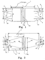
- Optische Abzweigmultiplexereinrichtung, die wenigstens einen MMI-Hohlleiter und wenigstens zwei sogenannte Zugangshohlleiter (1, 2), die auf einer ersten Seite des MMI-Hohlleiters angeordnet sind, und wenigstens einen Zugangshohlleiter (3, 4), der auf einer zweiten Seite des MMI-Hohlleiters angeordnet ist, enthält, wobei die erste und die zweite Seite kurze Seiten des MMI-Hohlleiters sind, wobei die kurzen Seiten kürzer als wenigstens eine weitere Seite des MMI-Hohlleiters sind; dadurch gekennzeichnet, dass die Zugangshohlleiter (1, 2, 3, 4) eine sogenannte Kegelstruktur haben, so dass die Zugangshohlleiter (1, 2, 3, 4) bei ihren Anschlüssen zum MMI-Hohlleiter breiter als an ihren freien Enden sind; und dass wenigstens eine Bragg-Gitterstruktur (50) im MMI-Hohlleiter angeordnet ist.
- Optische Abzweigmultiplexereinrichtung nach Anspruch 1, dadurch gekennzeichnet, dass die Bragg-Gitterstruktur (50) in der Mitte des MMI-Hohlleiters angeordnet ist.
- Optische Abzweigmultiplexereinrichtung nach Anspruch 1, dadurch gekennzeichnet, dass die Bragg-Gitterstruktur (50) in Bezug auf die Mittenlinie des MMI-Hohlleiters versetzt ist, welche Mittenlinie senkrecht zu der Richtung einer Ausbreitung von Licht im MMI-Hohlleiter ist.
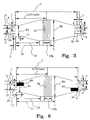
- Optische Abzweigmultiplexereinrichtung nach Anspruch 2 oder 3, dadurch gekennzeichnet, dass die Vorrichtung ein thermisch, optisch oder elektrisch aktives Phasensteuerelement enthält.
- Optische Abzweigmultiplexereinrichtung nach Anspruch 4, dadurch gekennzeichnet, dass der MMI-Hohlleiter eine Kegelstruktur auf jeder Seite der Bragg-Gitterstruktur (50) hat, so dass der MMI-Hohlleiter bei seinem Anschluss zu der Bragg-Gitterstruktur breiter als an seinem anderen Ende ist.
- Optische Abzweigmultiplexereinrichtung nach Anspruch 5, dadurch gekennzeichnet, dass die Kegelstruktur an dem MMI-Hohlleiter linear ist.
- Optische Abzweigmultiplexereinrichtung nach Anspruch 5, dadurch gekennzeichnet, dass die Kegelstruktur an dem MMI-Hohlleiter parabolisch ist.
- Optische Abzweigmultiplexereinrichtung nach Anspruch 6 oder 7, dadurch gekennzeichnet, dass wenigstens ein Zugangshohlleiter (1) auf der einen Seite des MMI-Hohlleiters so angeordnet ist, dass die optische Pfadlänge dieses Zugangshohlleiters unterschiedlich von den optischen Pfadlängen der übrigen Zugangshohlleiter (2, 3, 4) sein wird.
- Optische Abzweigmultiplexereinrichtung nach Anspruch 6 oder 7, dadurch gekennzeichnet, dass sie wenigstens drei Zugangshohlleiter (1, 2, 3, 4) hat und dass wenigstens ein Zugangshohlleiter (1, 3) auf der ersten und der zweiten Seite des MMI-Hohlleiters so angeordnet ist, dass die optischen Pfadlängen des wenigstens einen Zugangshohleiters, der auf der ersten und der zweiten Seite des MMI-Hohlleiters angeordnet ist, unterschiedlich von den optischen Pfadlängen der übrigen Zugangshohlleiter (2, 4) ist.
- Optische Abzweigmultiplexereinrichtung nach Anspruch 8 oder 9, dadurch gekennzeichnet, dass ein Zugangshohlleiter an einem ersten MMI-Hohlleiter mit einem Zugangshohlleiter an einem zweiten MMI-Hohlleiter gekoppelt ist.
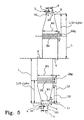
- Optische Abzweigmultiplexereinrichtung nach Anspruch 1, dadurch gekennzeichnet, dass ein Teil (60) des MMI-Hohlleiters benachbart zu wenigstens einem Zugangshohlleiter im MMI-Hohlleiter einen Brechungsindex hat, der unterschiedlich von dem Brechungsindex von übrigen Teilen des MMI-Hohlleiters ist.
- Optische Abzweigmultiplexereinrichtung nach Anspruch 11, dadurch gekennzeichnet, dass die Vorrichtung wenigstens zwei MMI-Hohlleiter und wenigstens zwei Bragg-Gitterstrukturen (50) enthält, wobei wenigstens ein sogenannter Zugangshohlleiter (1, 2) auf einer ersten Seite eines ersten MMI-Hohlleiters angeordnet ist und wenigstens ein Zugangshohlleiter (3, 4) auf einer zweiten Seite eines zweiten MMI-Hohlleiters angeordnet ist und wobei die erste und die zweite Seite kurze Seiten des MMI-Hohlleiters sind, wobei die kurzen Seiten kürzer als wenigstens eine weitere Seite des MMI-Hohlleiters sind; dass eine zweite kurze Seite des ersten MMI-Hohlleiters und eine erste Seite des zweiten MMI-Hohlleiters wechselseitig gekoppelt sind; dass die Zugangshohlleiter eine sogenannte Kegelstruktur haben, so dass die Zugangshohlleiter (1, 2, 3, 4) bei ihren Anschlüssen zu dem MMMI-Hohlleiter breiter als an ihren freien Enden sind; und dass die Bragg-Gitterstrukturen in den MMI-Hohlleitern angeordnet sind.
- Optische Abzweigmultiplexereinrichtung nach Anspruch 12, dadurch gekennzeichnet, dass die zweite Seite des ersten MMI-Hohlleiters und die erste Seite des zweiten MMI-Hohlleiters in Bezug zueinander lateral versetzt sind.
- Optische Abzweigmultiplexereinrichtung nach Anspruch 13, dadurch gekennzeichnet, dass die MMI-Hohlleiter eine Kegelstruktur auf jeder Seite der Bragg-Gitterstrukturen (50) haben, so dass die MMI-Hohlleiter bei ihren Anschlüssen zu der Bragg-Gitterstruktur breiter als an ihrem anderen Ende sind.
Applications Claiming Priority (4)
| Application Number | Priority Date | Filing Date | Title |
|---|---|---|---|
| SE9700829 | 1997-03-07 | ||
| SE9700829A SE520432C2 (sv) | 1997-03-07 | 1997-03-07 | Optisk anordning för våglängdsmultiplexering/demultiplexering innefattande MMI-vågledare och Braggreflektorstruktur. |
| US09/033,092 US6047096A (en) | 1997-03-07 | 1998-03-02 | Optical device |
| PCT/SE1998/000393 WO1998039679A1 (en) | 1997-03-07 | 1998-03-05 | Optical wavelength selective device including at least one bragg-grating structure_____ |
Publications (2)
| Publication Number | Publication Date |
|---|---|
| EP0965060A1 EP0965060A1 (de) | 1999-12-22 |
| EP0965060B1 true EP0965060B1 (de) | 2008-01-09 |
Family
ID=26662925
Family Applications (1)
| Application Number | Title | Priority Date | Filing Date |
|---|---|---|---|
| EP98908412A Expired - Lifetime EP0965060B1 (de) | 1997-03-07 | 1998-03-05 | Wellenlängenselektive optische vorrichtung mit mindestens einer bragg-gitterstruktur |
Country Status (5)
| Country | Link |
|---|---|
| US (1) | US6047096A (de) |
| EP (1) | EP0965060B1 (de) |
| CN (1) | CN1120380C (de) |
| AU (1) | AU6644598A (de) |
| WO (1) | WO1998039679A1 (de) |
Families Citing this family (28)
| Publication number | Priority date | Publication date | Assignee | Title |
|---|---|---|---|---|
| JP2000056153A (ja) * | 1998-08-12 | 2000-02-25 | Kdd Corp | 波長フィルタ |
| SE514820C2 (sv) * | 1999-02-19 | 2001-04-30 | Ericsson Telefon Ab L M | Våglängdsselektiv modulator och förfarande för modulering av optiska våglängdskanaler |
| US6587615B1 (en) * | 1999-05-11 | 2003-07-01 | Jds Fitel Inc. | Wavelength multiplexer-demultiplexer having a wide flat response within the spectral passband |
| US6421478B1 (en) * | 1999-05-11 | 2002-07-16 | Jds Fitel Inc. | Tapered MMI coupler |
| US6317256B1 (en) * | 2000-02-15 | 2001-11-13 | Trw Inc. | Method of gain and noise figure equalization for simultaneous optical splitter/amplifier |
| US6571038B1 (en) * | 2000-03-01 | 2003-05-27 | Lucent Technologies Inc. | Multimode interference coupler with tunable power splitting ratios and method of tuning |
| GB2368131A (en) * | 2000-10-11 | 2002-04-24 | Marconi Caswell Ltd | Flared optical waveguide coupler |
| US6563988B2 (en) * | 2001-04-25 | 2003-05-13 | Lightwave Microsystems Corporation | Optical apparatus and method having predetermined group velocity dispersion |
| IL145320A (en) * | 2001-09-06 | 2006-12-10 | Gilad Optical Switches Ltd | Tunable optical filter |
| DE10145277B4 (de) * | 2001-09-14 | 2007-04-05 | Photeon Technologies Gmbh | Optischer Wellenleiter mit Taper und Wellenlängenmultiplexer/-demultiplexer mit einem solchen Wellenleiter oder solchen Wellenleitern |
| WO2003042737A2 (en) * | 2001-11-15 | 2003-05-22 | UNIVERSITé LAVAL | Array grating filters as segmented waveguide |
| US6993224B1 (en) | 2001-11-15 | 2006-01-31 | UNIVERSITé LAVAL | Segmented waveguide array gratings (SWAG)-based archival optical memory |
| GB2384572A (en) * | 2002-01-25 | 2003-07-30 | Denselight Semiconductors Pte | Optical waveguide tap with multimode interferometer(MMI) |
| TW594090B (en) | 2003-05-20 | 2004-06-21 | Univ Nat Taiwan Normal | SOI integrated reconfigurable optical add/drop multiplexer and manufacturing method thereof |
| WO2005022223A1 (ja) * | 2003-08-28 | 2005-03-10 | Nec Corporation | 導波路型光デバイスおよびその製造方法 |
| CN100409049C (zh) * | 2004-05-28 | 2008-08-06 | 日立化成工业株式会社 | 包含光波导的光学系统 |
| WO2005116703A1 (ja) * | 2004-05-28 | 2005-12-08 | Hitachi Chemical Company, Ltd. | 光導波路を含む光システム |
| JP5454256B2 (ja) * | 2010-03-17 | 2014-03-26 | 富士通株式会社 | 光導波路素子及びそのような光導波路素子を備えた光受信機 |
| GB2488308A (en) * | 2011-01-19 | 2012-08-29 | Univ Surrey | Optical Filter |
| US20150086158A1 (en) * | 2013-09-26 | 2015-03-26 | Mitsubishi Electric Corporation | Multi-Mode Phase-Shifting Interference Device |
| JP6711025B2 (ja) * | 2016-03-03 | 2020-06-17 | 株式会社豊田中央研究所 | グレーティングカプラ、グレーティングカプラアレイ、結像光学系、光スキャナ、及びレーザレーダ装置 |
| CN105572796B (zh) * | 2016-03-07 | 2018-08-21 | 龙岩学院 | 一种基于反对称多模布拉格波导光栅的上下路滤波器 |
| CN105759362A (zh) * | 2016-05-13 | 2016-07-13 | 龙岩学院 | 一种基于反对称多模布拉格波导光栅的带通带阻滤波器 |
| WO2018198193A1 (ja) * | 2017-04-25 | 2018-11-01 | 三菱電機株式会社 | 半導体装置および半導体装置の製造方法 |
| CN107092056B (zh) * | 2017-06-12 | 2019-07-05 | 北京大学 | 一种波分复用/解复用器及其制作方法 |
| WO2018227556A1 (zh) * | 2017-06-16 | 2018-12-20 | 华为技术有限公司 | 一种光分插复用器 |
| CN110703385B (zh) * | 2019-11-11 | 2021-04-02 | 西湖大学 | 基于光散射的图案化的多模干涉耦合器、设计方法和应用 |
| US11609392B1 (en) * | 2022-02-24 | 2023-03-21 | X Development Llc | Photonic coupler |
Citations (3)
| Publication number | Priority date | Publication date | Assignee | Title |
|---|---|---|---|---|
| JPS6215879A (ja) * | 1985-07-12 | 1987-01-24 | Sharp Corp | 半導体レ−ザアレイ装置 |
| WO1996008044A2 (en) * | 1994-09-06 | 1996-03-14 | Philips Electronics N.V. | Optoelectronic semiconductor device with a semiconductor diode laser |
| EP0826988A2 (de) * | 1996-08-27 | 1998-03-04 | Lucent Technologies Inc. | Integriert optische Notchfilter |
Family Cites Families (7)
| Publication number | Priority date | Publication date | Assignee | Title |
|---|---|---|---|---|
| DE2930681A1 (de) * | 1979-07-28 | 1981-02-12 | Licentia Gmbh | Anordnung zum filtern, verzweigen, schalten oder modulieren von signalen in vielwelligen optischen wellenleitern |
| US5093876A (en) * | 1990-07-27 | 1992-03-03 | At&T Bell Laboratories | WDM systems incorporating adiabatic reflection filters |
| GB2280968B (en) * | 1993-08-12 | 1996-07-31 | Northern Telecom Ltd | Chirped optical fibre filter |
| GB9323226D0 (en) * | 1993-11-10 | 1994-01-05 | Northern Telecom Ltd | Optical fibre elements |
| GB9420132D0 (en) * | 1994-10-05 | 1994-11-16 | Norhern Telecom Limited | Optical amplifiers |
| GB9423105D0 (en) * | 1994-11-16 | 1995-01-04 | Northern Telecom Ltd | Optical wave grating filter |
| SE503514C2 (sv) * | 1995-02-06 | 1996-07-01 | Ericsson Telefon Ab L M | Anordning och förfarande för att koppla en eller flera våglängdskanaler till och från en optisk fiber |
-
1998
- 1998-03-02 US US09/033,092 patent/US6047096A/en not_active Expired - Lifetime
- 1998-03-05 CN CN98803161A patent/CN1120380C/zh not_active Expired - Fee Related
- 1998-03-05 WO PCT/SE1998/000393 patent/WO1998039679A1/en active IP Right Grant
- 1998-03-05 AU AU66445/98A patent/AU6644598A/en not_active Abandoned
- 1998-03-05 EP EP98908412A patent/EP0965060B1/de not_active Expired - Lifetime
Patent Citations (3)
| Publication number | Priority date | Publication date | Assignee | Title |
|---|---|---|---|---|
| JPS6215879A (ja) * | 1985-07-12 | 1987-01-24 | Sharp Corp | 半導体レ−ザアレイ装置 |
| WO1996008044A2 (en) * | 1994-09-06 | 1996-03-14 | Philips Electronics N.V. | Optoelectronic semiconductor device with a semiconductor diode laser |
| EP0826988A2 (de) * | 1996-08-27 | 1998-03-04 | Lucent Technologies Inc. | Integriert optische Notchfilter |
Non-Patent Citations (1)
| Title |
|---|
| PATENT ABSTRACTS OF JAPAN vol. 011, no. 187 (E - 516) 16 June 1987 (1987-06-16) * |
Also Published As
| Publication number | Publication date |
|---|---|
| WO1998039679A1 (en) | 1998-09-11 |
| CN1249820A (zh) | 2000-04-05 |
| AU6644598A (en) | 1998-09-22 |
| US6047096A (en) | 2000-04-04 |
| CN1120380C (zh) | 2003-09-03 |
| EP0965060A1 (de) | 1999-12-22 |
Similar Documents
| Publication | Publication Date | Title |
|---|---|---|
| EP0965060B1 (de) | Wellenlängenselektive optische vorrichtung mit mindestens einer bragg-gitterstruktur | |
| Smit et al. | PHASAR-based WDM-devices: Principles, design and applications | |
| US6005992A (en) | Optical device | |
| KR19980044384A (ko) | 광 디멀티플렉서 | |
| US5054873A (en) | High density integrated optical multiplexer/demultiplexer | |
| CA2282421C (en) | Optical wavelength selective device including at least one bragg-grating structure | |
| US6571031B1 (en) | Device for multiplexing/demultiplexing and method therewith | |
| US6449411B1 (en) | Optical wavelength tunable filter | |
| JP3703401B2 (ja) | 光波回路モジュール | |
| KR100327898B1 (ko) | 직선형광도파로를구비한파장역다중화소자 | |
| KR100417001B1 (ko) | 보조 광도파로를 구비한 광세기 분할기 | |
| EP1451959B1 (de) | Einrichtung auf mmi-basis | |
| US7330658B2 (en) | Device and method for optical add/drop multiplexing | |
| EP1159646B1 (de) | Wellenlängenselektiver modulator | |
| US7403682B1 (en) | Dispersion compensation apparatus | |
| JP3966401B2 (ja) | 導波路型光合波器とこれを用いた多波長光源 | |
| US20020067881A1 (en) | Polarization independent coupler with bragg-evanescent-coupler grating | |
| EP0947861A1 (de) | Hybrides wellenführendes optisches Element | |
| EP1091220B1 (de) | Verbreiterung der Brandbreite eines Wellenleitergitters | |
| Okawa et al. | Low loss and wide passband arrayed waveguide grating demultiplexer | |
| JP3396477B2 (ja) | 集積光導波回路 | |
| JP2003315575A (ja) | 光合波器 | |
| JP2003315574A (ja) | 光合分波器 |
Legal Events
| Date | Code | Title | Description |
|---|---|---|---|
| PUAI | Public reference made under article 153(3) epc to a published international application that has entered the european phase |
Free format text: ORIGINAL CODE: 0009012 |
|
| 17P | Request for examination filed |
Effective date: 19991007 |
|
| AK | Designated contracting states |
Kind code of ref document: A1 Designated state(s): DE ES FI FR GB IT NL SE |
|
| RAP1 | Party data changed (applicant data changed or rights of an application transferred) |
Owner name: TELEFONAKTIEBOLAGET LM ERICSSON (PUBL) |
|
| 17Q | First examination report despatched |
Effective date: 20041207 |
|
| 17Q | First examination report despatched |
Effective date: 20041207 |
|
| GRAP | Despatch of communication of intention to grant a patent |
Free format text: ORIGINAL CODE: EPIDOSNIGR1 |
|
| GRAS | Grant fee paid |
Free format text: ORIGINAL CODE: EPIDOSNIGR3 |
|
| GRAA | (expected) grant |
Free format text: ORIGINAL CODE: 0009210 |
|
| AK | Designated contracting states |
Kind code of ref document: B1 Designated state(s): DE ES FI FR GB IT NL SE |
|
| REG | Reference to a national code |
Ref country code: GB Ref legal event code: FG4D |
|
| REF | Corresponds to: |
Ref document number: 69838977 Country of ref document: DE Date of ref document: 20080221 Kind code of ref document: P |
|
| PG25 | Lapsed in a contracting state [announced via postgrant information from national office to epo] |
Ref country code: NL Free format text: LAPSE BECAUSE OF FAILURE TO SUBMIT A TRANSLATION OF THE DESCRIPTION OR TO PAY THE FEE WITHIN THE PRESCRIBED TIME-LIMIT Effective date: 20080109 |
|
| NLV1 | Nl: lapsed or annulled due to failure to fulfill the requirements of art. 29p and 29m of the patents act | ||
| PG25 | Lapsed in a contracting state [announced via postgrant information from national office to epo] |
Ref country code: FI Free format text: LAPSE BECAUSE OF FAILURE TO SUBMIT A TRANSLATION OF THE DESCRIPTION OR TO PAY THE FEE WITHIN THE PRESCRIBED TIME-LIMIT Effective date: 20080109 Ref country code: ES Free format text: LAPSE BECAUSE OF FAILURE TO SUBMIT A TRANSLATION OF THE DESCRIPTION OR TO PAY THE FEE WITHIN THE PRESCRIBED TIME-LIMIT Effective date: 20080420 |
|
| ET | Fr: translation filed | ||
| PG25 | Lapsed in a contracting state [announced via postgrant information from national office to epo] |
Ref country code: SE Free format text: LAPSE BECAUSE OF FAILURE TO SUBMIT A TRANSLATION OF THE DESCRIPTION OR TO PAY THE FEE WITHIN THE PRESCRIBED TIME-LIMIT Effective date: 20080409 |
|
| PLBE | No opposition filed within time limit |
Free format text: ORIGINAL CODE: 0009261 |
|
| STAA | Information on the status of an ep patent application or granted ep patent |
Free format text: STATUS: NO OPPOSITION FILED WITHIN TIME LIMIT |
|
| 26N | No opposition filed |
Effective date: 20081010 |
|
| PG25 | Lapsed in a contracting state [announced via postgrant information from national office to epo] |
Ref country code: IT Free format text: LAPSE BECAUSE OF FAILURE TO SUBMIT A TRANSLATION OF THE DESCRIPTION OR TO PAY THE FEE WITHIN THE PRESCRIBED TIME-LIMIT Effective date: 20080109 |
|
| PGFP | Annual fee paid to national office [announced via postgrant information from national office to epo] |
Ref country code: FR Payment date: 20140317 Year of fee payment: 17 |
|
| PGFP | Annual fee paid to national office [announced via postgrant information from national office to epo] |
Ref country code: GB Payment date: 20140327 Year of fee payment: 17 |
|
| PGFP | Annual fee paid to national office [announced via postgrant information from national office to epo] |
Ref country code: DE Payment date: 20140327 Year of fee payment: 17 |
|
| REG | Reference to a national code |
Ref country code: DE Ref legal event code: R119 Ref document number: 69838977 Country of ref document: DE |
|
| GBPC | Gb: european patent ceased through non-payment of renewal fee |
Effective date: 20150305 |
|
| REG | Reference to a national code |
Ref country code: FR Ref legal event code: ST Effective date: 20151130 |
|
| PG25 | Lapsed in a contracting state [announced via postgrant information from national office to epo] |
Ref country code: DE Free format text: LAPSE BECAUSE OF NON-PAYMENT OF DUE FEES Effective date: 20151001 Ref country code: GB Free format text: LAPSE BECAUSE OF NON-PAYMENT OF DUE FEES Effective date: 20150305 |
|
| PG25 | Lapsed in a contracting state [announced via postgrant information from national office to epo] |
Ref country code: FR Free format text: LAPSE BECAUSE OF NON-PAYMENT OF DUE FEES Effective date: 20150331 |