EP0962046B1 - Anordnung und verfahren zum herabsetzen von interferenzen bei trägerruckgewinnung für digitale demodulierung - Google Patents
Anordnung und verfahren zum herabsetzen von interferenzen bei trägerruckgewinnung für digitale demodulierung Download PDFInfo
- Publication number
- EP0962046B1 EP0962046B1 EP98903523A EP98903523A EP0962046B1 EP 0962046 B1 EP0962046 B1 EP 0962046B1 EP 98903523 A EP98903523 A EP 98903523A EP 98903523 A EP98903523 A EP 98903523A EP 0962046 B1 EP0962046 B1 EP 0962046B1
- Authority
- EP
- European Patent Office
- Prior art keywords
- frequency
- carrier
- signal
- harmonic
- lock
- Prior art date
- Legal status (The legal status is an assumption and is not a legal conclusion. Google has not performed a legal analysis and makes no representation as to the accuracy of the status listed.)
- Expired - Lifetime
Links
Images


Classifications
-
- H—ELECTRICITY
- H03—ELECTRONIC CIRCUITRY
- H03D—DEMODULATION OR TRANSFERENCE OF MODULATION FROM ONE CARRIER TO ANOTHER
- H03D7/00—Transference of modulation from one carrier to another, e.g. frequency-changing
- H03D7/16—Multiple-frequency-changing
-
- H—ELECTRICITY
- H03—ELECTRONIC CIRCUITRY
- H03J—TUNING RESONANT CIRCUITS; SELECTING RESONANT CIRCUITS
- H03J1/00—Details of adjusting, driving, indicating, or mechanical control arrangements for resonant circuits in general
- H03J1/0008—Details of adjusting, driving, indicating, or mechanical control arrangements for resonant circuits in general using a central processing unit, e.g. a microprocessor
-
- H—ELECTRICITY
- H03—ELECTRONIC CIRCUITRY
- H03J—TUNING RESONANT CIRCUITS; SELECTING RESONANT CIRCUITS
- H03J7/00—Automatic frequency control; Automatic scanning over a band of frequencies
- H03J7/02—Automatic frequency control
-
- H—ELECTRICITY
- H03—ELECTRONIC CIRCUITRY
- H03D—DEMODULATION OR TRANSFERENCE OF MODULATION FROM ONE CARRIER TO ANOTHER
- H03D7/00—Transference of modulation from one carrier to another, e.g. frequency-changing
- H03D7/16—Multiple-frequency-changing
- H03D7/165—Multiple-frequency-changing at least two frequency changers being located in different paths, e.g. in two paths with carriers in quadrature
-
- H—ELECTRICITY
- H03—ELECTRONIC CIRCUITRY
- H03J—TUNING RESONANT CIRCUITS; SELECTING RESONANT CIRCUITS
- H03J2200/00—Indexing scheme relating to tuning resonant circuits and selecting resonant circuits
- H03J2200/31—Several sweeping or scanning speeds
Definitions
- This invention described herein relates generally to the demodulation of digital signals. More particularly, the invention described herein relates to controlling a down conversion frequency to account for harmonics resident in a demodulator.
- Demodulation is a widely used process to make very high frequencies usable.
- One of the carrier recovery techniques in digital demodulation is based on the presence of a VCO (Voltage Controlled Oscillator) in the recovery loop.
- the VCO performs two functions: first, it searches for the carrier frequency in a procedure called a "frequency sweep" and second it tracks the carrier once the recovery loop locks. This is important as the frequency offset that it tracks might be up to +/-5 MHz. This frequency drift is mostly caused by low noise amplifier drift (LNA).
- LNA low noise amplifier drift
- Harmonics are generally additional spectral components which can interfere with a carrier recovery loop.
- a major problem is the chance that oscillator harmonics are present in the neighborhood of the VCO. If the harmonics fall within the capture/ tracking range of the carrier recovery loop, there is a chance that (due to coupling) the VCO will become disturbed and either fail to lock or break lock once acquired. Measurements show that this interference could cause from 1 to 5 dB loss. Specifically, this interference may be high enough in some cases to make the acquisition impossible (if the IF carrier falls over the harmonic) or to desynchronize the demodulator or the FEC decoder (if tracking polls the VCO frequency over the harmonic) especially when operating in noisy channel.
- the present invention overcomes the aforementioned problems as it accommodates for harmonics in various frequency bands.
- the disclosed system is useful in satellite receiver and cable television receivers which require the recovery of a carrier signal.
- the system and method disclosed herein solves the problems of interference by various harmonics by locking onto a down converted carrier, and if no lock, then by locking on to an offset version of the down converted carrier.
- the system and method relocates the down converted carrier to a new location on the swept frequency band, far away from the harmonic and other degrading frequencies (for example, the roll off frequency of a SAW filter).
- a demodulator will function properly even in the presence of degrading harmonics.
- FIG. 1 shows a block diagram of different components as contemplated by the present invention.
- An L-band digital signal 101 is received from a digital source (for example, a satellite receiver) and tracked by a tracking filter 102.
- additional inputs of digital source include digital cable distribution systems.
- non-digital inputs are received as well including from analog television systems as well as from radio transmission systems. These systems are only given as examples.
- the application of the invention described herein is contemplated for a variety of uses where harmonic signals exists and need to be accommodated.
- the output of the tracking filter 102 is fed through controlled amplifier 103.
- Controlled amplifier is controlled by demodulation control 115 for automatic gain control purposes.
- the output of controlled amplifier is fed into mixer 104 where it is down converted into an intermediate frequency (IF).
- Mixer 104 uses a signal output from synthesizer 107.
- the output of synthesizer 107 is controlled to be a set frequency.
- synthesizer 107 is controlled to output a signal at a first frequency and, upon control from microprocessor 122, output the signal at a second frequency.
- the two frequencies are referred to as f(synth) and f(synth-delta) where delta is an offset which changes the output of synthesizer 107.
- microprocessor 122 outputs one of at least two signals of SYNTH, and SYNTH-DELTA.
- the output from mixer 104 is passed through standing acoustical wave (SAW) filter 105 where the IF signal is filtered to remove unwanted characteristics.
- IF signal is passed through amplifier 106 and then to a baseband processing system.
- SAW standing acoustical wave
- Baseband processing system contains a number of different sub-circuits.
- the output from amplifier 106 is split into two paths I and Q, where I represents the in-phase component of the IF signal and Q represents the quadrature component of the IF signal.
- I represents the in-phase component of the IF signal
- Q represents the quadrature component of the IF signal.
- IF signal is mixed at mixer 108 with a 90 degrees shifted output from voltage controlled oscillator 117 (VCO1).
- the phase shift is accomplished by phase shifter 110.
- the output from mixer 108 is passed through low pass filter (LPF) 111, through A/D converter 113, then to demodulation control 115.
- the path of Q is similar to that of I, using mixer 109, LPF 112, and A/D converter 114.
- the output of demodulation control 115 is fed into forward error correction circuit 116 and output as a desired signal.
- the desired signal output is contemplated to be an MPEG output signal.
- demodulation controller 115 evaluates the frequency F lock-int using the pre-scaled signal from VCO1 through DIV 123 to determine how close the VCO1 frequency is from the harmonic.
- the microprocessor changes the frequency of the synthesizer 107 with the offset value which will cause carrier recovery lock at a frequency between the harmonic and the limit where the filtering (SAW or baseband) starts degrading the spectrum of the signal.
- the sweep signal is enabled thereafter but with a much smaller amplitude as the system knows approximately where the frequency F final-lock is.
- the narrow sweep only has to be wider than the synthesizer step. In this way, the acquisition at the new frequency F lock-final is done much faster then the initial one at F lock-int .
- Demodulation control 115 outputs a variety of control signals. First, it outputs an automatic gain control signal, passed through LPF 121, which controls amplifier 103, discussed above. Second, demodulation control 115 outputs a carrier recovery loop signal, passed through LPF 120, for VCO1 117. Finally, demodulation control 115 outputs symbol clock recovery signal, passed through LPF 119, for VCO2 118 so as to enable A/D converters 113 and 114 to know when each symbol to be decoded starts. To assist in the symbol clock recovery loop, the demodulation controller uses divider DIV 123 to scale down the frequency from VCO1 117 to determine what the clock recovery frequency out to VCO2 118 should be.
- the most prevalent harmonic arises from this loop including VCO2 118. It is this harmonic for which the present invention accounts. However, other harmonics exist as well and are, likewise, avoided. Further, harmonics may arise from external locations (for example, from a timing circuit in another microprocessor). Embodiments of the present invention further contemplate avoiding these additional harmonics as well.
- microprocessor 122 In addition to controlling synthesizer 107, microprocessor 122 also controls demodulation control 115 and forward error correction 116.
- the carrier recovery circuitry performs two main functions: it searches for a down-converted carrier frequency through a procedure referred to as "frequency sweep" and it tracks the carrier once the recovery loop locks. As to the tracking function, the carrier recovery circuitry is enabled to track frequency drifts up to +/- 5 MHz. These drifts are mostly caused by low noise amplifier (LNA) drift.
- LNA low noise amplifier
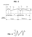
- Figure 2 shows the voltage output signal to VCOI 117 as contemplated by embodiments of the present invention.
- Figure 2 shows two sets of frequency sweeps. The first is referred to the period of f(synth). This period includes two equal time intervals t 1 and a time interval t 2 . These two time intervals show the voltage output from VCO1 117 as having two slopes m 1 (and -m 1 ) and m 2 .
- the offset frequency period f(synth-delta) and as the offset frequency is set so as to include the carrier frequency, the length of the internal time periods t 3 and t 4 are adjusted to be much shorter.
- embodiments of the present invention contemplate the slopes m 1 and m 2 of the voltage waveform input into VCO1 117 as remaining the same values.
- the sweep signal as shown in Figure 2 has the two different slopes m 1 and m 2 so the resulting sweep is slow enough (m 2 ) to lock on the carrier signal at the worst signal to noise ratio (SNR) that the system is specified to work.
- SNR signal to noise ratio
- the sweep (m 1 ) is allowed to be relatively fast in order to minimize the acquisition time of the carrier.
- Embodiments of the present invention contemplate the voltage provided by the demodulation controller to the VCO1 117 as ideally linear. Alternatively, non-linear sweeps are envisioned as well as to allow for precise control over the sweeping interval.
- the peak to peak value of the signal of Figure 2 determines the frequency swing around the expected IF carrier (as generally represented at 480 MHz for terrestrial applications or 70 MHz in satellite receivers).
- the f(synth) period is followed by the f(synth-delta) period.
- the alteration of one waveform then the other wave form allows for fast acquisition of the down converted carrier signal as, if the carrier is not acquired during the f(synth) period, then altering the down conversion carrier frequency may likely acquire the carrier during the f(synth-delta) period.
- the present invention contemplates sweeping with the f(synth) period multiple times before switching to the f(synth-delta) period. This method allows for system averaging accounting for transient reception effects (for example, temporary blockage of the carrier signal).
- the present invention contemplates a third scheme for initiating the f(synth-delta) period where the f(synth-delta) is only initiated after an established lock and subsequent failure (for example, when the carrier frequency shifts due to LNA).
- Figure 3 shows the output of VCO1 117 during the harmonic avoidance scheme.
- F saw(min) and F saw(max) represent the minimum and maximum frequencies allowed to pass through SAW filter 105. Accordingly, all down converted carriers frequencies should be controlled to fall within this range. Further, embodiments of the present invention contemplate keeping, for example, F min apart from F saw(min) because of the relatively fast roll off of signal strength near the edges of the SAW filter's cut off frequencies.
- VCO1 117 sweeps through its controlled frequency range F min to F max . As shown here, the harmonic frequency f harmonic is close to the actual down converted carrier frequency F lock-int .
- the carrier recovery loop with VCO1 may, as shown here, or may not actually lock onto the down converted carrier signal, the closeness of the harmonic frequency to the carrier frequency may disrupt the operation of the carrier recovery loop.
- the carrier recovery loop looses lock at time t d .
- the microprocessor (or micro controller) 122 alters the synthesizer's down converting frequency from F(synth) to F(synth-delta).
- the carrier recovery loop starts sweeping for the carrier using shorter intervals at time t d .
- the final lock is achieved onto the down converted carrier frequency.
- the carrier recovery loop will eventually lock and a true/ false lock decision is made by the controller or by the microprocessor. If the lock is not onto the proper carrier (for example, a false lock onto an alternate phase of the carrier), then the system breaks lock until the correct lock is achieved. Also, if too many errors are generated by the harmonic, through reducing the SNR beyond a threshold level, the system again breaks lock and repeats the acquisition process until a true lock has been achieved.
- the true/false lock determination is described in greater detail in U.S. Serial No. 08/427,660, entitled “Method And Apparatus For Locating And Tracking A QPSK Carrier” which is a continuation of U.S. Serial No. 08/160.839, entitled “Method And Apparatus For Locating And Tracking A QPSK Carrier", now abandoned, which is incorporated by reference for all necessary disclosure.
- the forming and breaking of lock is shown as the frequency F lock-int .
- the present invention contemplates that the frequency sweep range (from F min to F max ) to be larger than the expected LNA offset plus the synthesizer resolution step and SAW filter. Also, embodiments of the present invention contemplate baseband LPF should not distort the spectrum of the signal. Also, for noise reduction purposes, embodiments of the present invention contemplate separating F min and F max from the cut off frequencies (F saw(min) and F saw(max) of the SAW filter because of signal degradation near these cut off frequencies. Therefore, the system offers enough clearance from the distortion at F saw(min) and F saw(max) so as to accommodate the sweep and the lock of the carrier recovery loop even at the extreme of the sweep cycle.
- the shifted carrier frequency is adjusted so as to be as far away from degrading frequencies as possible.
- the carrier frequency is adjusted to be equally between the initial lock frequency (which failed previously to lock) F lock-int and one of the frequencies of SAW filter F saw(min) .
- F saw(min) is preferable to move to as the harmonic is closer to F saw(max) that F saw(min) .
- the F lock-final frequency is moved in the direction of F saw(max) to avoid a harmonic closer to F saw(min) .
- the F harmonic frequency and at least one of the F min and F max frequencies are used to place the F lock-final frequency.
- the frequencies in which to avoid are those containing degrading characteristics.
- the frequency of F min was chosen over the frequency F saw(min) in one example (and reversed in another example) as determining which set of frequencies to use is system specific as to avoid noisy frequencies. For instance, if F saw(min) was far from F min , then present embodiments of the invention contemplate F min as the lower frequency limit as moving too far in the direction of F saw(min) may extend F final-lock below F min . The same process is readily applied to the upper frequencies as well.
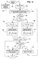
- Figure 4 shows a flowchart as contemplated by embodiments of the present invention.
- the system determines whether a harmonic is present which may disrupt carrier recovery operations. If there is no carrier, the system (for example, an integrated receiver-decoder) locks onto the down converted carrier using regular procedures as shown above with respect to Figure 1, as shown by step 402. If there is a harmonic signal present, then the system determines (for example, through a sensing operation of microprocessor 122 or through manual input of internal clock frequencies) the frequency of the harmonic (or harmonics, as the case may be). The system next attempts to lock the carrier recovery unit onto the carrier signal at step 404.
- a harmonic for example, an integrated receiver-decoder
- the tuner is controlled to sweep in the wide fast/slow sweep using alternating frequency offsets.
- the frequency offset is 250 kHz.
- Figure 5 shows the wide fast/slow sweep pattern centered about, for example 480 MHz.
- An example of the 250 kHz offset applied is shown in Figure 6 by the inclusion of delta, in one cycle.
- the carrier should be locked, albeit possibly near the harmonic frequency.
- step 405 the frequency of the VCO1 is read through divider 123.
- the next portion of the carrier locking scheme as shown in Figure 4 relates to separating the carrier's down converted frequency from the harmonic frequency.
- the scheme determines if the harmonic frequency is above or below the down converted carrier frequency.
- the center frequency for the narrow sweep as shown through time periods t d through t j in Figure 3 is determined. It should be noted that, in this example, the frequency of the synthesizer is placed above that of the received signals. If, however, one desired to have the frequency of the synthesizer placed below that of the received signals, the equations used would be similar but with minor modifications as apparent to one of ordinary skill in the art.
- new frequency of the synthesizer 107 is determined as offset from the original frequency by f off as shown in step 411.
- the scheme sweeps for a number of cycles as shown in step 412.
- the number of sweeps is 4. This number is adjusted to account for any transient signals which may occur so as to maximize the chances for a new lock at the newly adjusted carrier frequency.
- the system determines whether the carrier recovery loop has locked. If yes, then as shown in step 414, the scheme determines if this is a proper lock, far from any problems (for example, locking on an out of phase false carrier or excessive error signals). If this is a good lock as determined in step 415, then the scheme loops back to step 414 to continue to monitor the quality of the lock.
- step 412 If not a good lock, the scheme loops back to step 412 until the limit on the number of sweep cycles is reached. From step 413, if no lock is found, then the system changes back to the wide sweep back at the original carrier down converted frequency shown here, for example, as the sweep centered at 480 MHz with a +/- 3 MHz sweep.
Claims (3)
- Demodulator mit einer Rückgewinnungsschleife, in der ein Oberschwingungssignal auf einer Oberschwingungsfrequenz die Erfassung oder Verfolgung eines Trägersignals unterbricht, mitdadurch gekennzeichnet, dass das Steuergerät den Frequenzgenerator so steuert, dass er das Signal auf einer zweiten Frequenz erzeugt, die von der ersten Frequenz abweicht, sodass die niedrigere Frequenz aus dem Wandler weiter von der Oberschwingungsfrequenz getrennt wird.einer Eingabe zum Empfangen eines Trägersignals auf einer mit einem Datensignal modulierten Trägerfrequenz,einem Frequenzgenerator zum Erzeugen eines Signals auf einer ersten Frequenz,einem Wandler zum Umwandeln des Trägersignals auf der Trägerfrequenz in eine niedrigere Frequenz in Reaktion auf das Signal vom Frequenzgenerator,einem Steuergerät zum Steuem des Frequenzgenerators undeiner Aufschaltungsschaltung zum Aufschalten auf die niedrigere Frequenz, wobei die Aufschaltungsschaltung die Quelle des Oberschwingungssignals ist,
- Demodulator nach Anspruch 1, dadurch gekennzeichnet, dass das Steuergerät feststellt, wie nahe die Oberschwingungsfrequenz an der abwärtsgewandelten Trägerfrequenz liegt.
- Demodulator nach Anspruch 1, dadurch gekennzeichnet, dass die Aufschaltungsschaltung zwei verschiedene Abtastzeiten zum Aufschalten auf die Trägerfrequenz verwendet.
Applications Claiming Priority (3)
| Application Number | Priority Date | Filing Date | Title |
|---|---|---|---|
| US3676997P | 1997-01-31 | 1997-01-31 | |
| US36769P | 1997-01-31 | ||
| PCT/US1998/000826 WO1998035544A2 (en) | 1997-01-31 | 1998-01-15 | System and method for harmonic interference avoidance in carrier recovery for digital demodulation |
Publications (3)
| Publication Number | Publication Date |
|---|---|
| EP0962046A2 EP0962046A2 (de) | 1999-12-08 |
| EP0962046A4 EP0962046A4 (de) | 1999-12-22 |
| EP0962046B1 true EP0962046B1 (de) | 2003-04-02 |
Family
ID=21890540
Family Applications (1)
| Application Number | Title | Priority Date | Filing Date |
|---|---|---|---|
| EP98903523A Expired - Lifetime EP0962046B1 (de) | 1997-01-31 | 1998-01-15 | Anordnung und verfahren zum herabsetzen von interferenzen bei trägerruckgewinnung für digitale demodulierung |
Country Status (8)
| Country | Link |
|---|---|
| US (1) | US6148039A (de) |
| EP (1) | EP0962046B1 (de) |
| JP (1) | JP2002501688A (de) |
| AU (1) | AU6027398A (de) |
| CA (1) | CA2279850A1 (de) |
| DE (1) | DE69812914T2 (de) |
| TW (1) | TW391114B (de) |
| WO (1) | WO1998035544A2 (de) |
Families Citing this family (10)
| Publication number | Priority date | Publication date | Assignee | Title |
|---|---|---|---|---|
| JPH11205172A (ja) | 1998-01-12 | 1999-07-30 | Alps Electric Co Ltd | 衛星放送受信機用チュ−ナ |
| CN1192496C (zh) * | 1999-03-11 | 2005-03-09 | 三菱电机株式会社 | 无线终端装置 |
| EP1063826A1 (de) * | 1999-06-25 | 2000-12-27 | Sony International (Europe) GmbH | Trägerrückgewinnungvorrichtung für ein digitales Quadratur-Signal |
| GB0020527D0 (en) | 2000-08-22 | 2000-10-11 | Mitel Semiconductor Ltd | Digital tuner |
| GB0210849D0 (en) * | 2002-05-11 | 2002-06-19 | Cedardell Ltd | Method of processing radio frequency signals and radio frequency receiver apparatus for use in such method |
| US7675996B2 (en) * | 2003-02-28 | 2010-03-09 | Johnson Richard A | Television receiver suitable for multi-standard operation and method therefor |
| WO2009115863A1 (en) * | 2008-03-19 | 2009-09-24 | Freescale Semiconductor, Inc. | Dc compensation for vlif signals |
| EP2343813B1 (de) | 2010-01-11 | 2013-05-15 | Elster | Verfahren und System zur Leistungsverwaltung von elektronischen Geräten |
| EP2343803B1 (de) * | 2010-01-11 | 2013-09-11 | Elster | Automatisches Frequenzoffsetkompensationsverfahren und Vorrichtung |
| US11165622B2 (en) * | 2019-10-18 | 2021-11-02 | Hughes Network Systems, LLC. | System and method for low-rate high-rate coupled acquisition and tracking of high symbol rate inroutes |
Family Cites Families (30)
| Publication number | Priority date | Publication date | Assignee | Title |
|---|---|---|---|---|
| US4000476A (en) * | 1974-12-19 | 1976-12-28 | Digital Communications Corporation | Phase locked loop with circuit for preventing sidelock |
| US4042884A (en) * | 1975-02-20 | 1977-08-16 | Rixon, Inc. | Phase demodulator with offset frequency reference oscillator |
| US4246546A (en) * | 1979-04-05 | 1981-01-20 | Motorola, Inc. | Apparatus and method for locking a PLL onto a selected offset frequency sideband |
| US4354277A (en) * | 1979-11-23 | 1982-10-12 | Trw Inc. | Signal acquisition system |
| US4314206A (en) * | 1979-12-26 | 1982-02-02 | Motorola Inc. | Noise chopper for preventing false locks in a coherent carrier recovery system |
| US4545072A (en) * | 1982-02-22 | 1985-10-01 | Motorola, Inc. | Method and apparatus for eliminating interference due to spurious signals generated in synthesized receivers |
| US4513448A (en) * | 1983-08-12 | 1985-04-23 | The United States Of America As Represented By The Secretary Of The Army | Low power radio synthesizer with harmonic identification feature |
| US4568888A (en) * | 1983-11-08 | 1986-02-04 | Trw Inc. | PLL Fast frequency synthesizer with memories for coarse tuning and loop gain correction |
| US4590440A (en) * | 1984-07-06 | 1986-05-20 | American Microsystems, Inc. | Phase locked loop with high and/or low frequency limit detectors for preventing false lock on harmonics |
| US4613825A (en) * | 1984-12-20 | 1986-09-23 | Motorola, Inc. | Rapid acquisition, tracking PLL with fast and slow sweep speeds |
| US4718117A (en) * | 1985-10-30 | 1988-01-05 | Capetronic (Bsr) Ltd. | TVRO receiver system with low-cost video-noise reduction filter |
| US4761825A (en) * | 1985-10-30 | 1988-08-02 | Capetronic (Bsr) Ltd. | TVRO earth station receiver for reducing interference and improving picture quality |
| US4876739A (en) * | 1985-10-30 | 1989-10-24 | Capetronic (Bsr) Ltd. | TVRO receiver system with low-cost video-noise reduction filter |
| JPH0810879B2 (ja) * | 1986-02-20 | 1996-01-31 | 富士通株式会社 | 復調装置 |
| JPH0710051B2 (ja) * | 1987-07-16 | 1995-02-01 | 八重洲無線株式会社 | 無線受信機 |
| DE3784930T2 (de) * | 1987-09-03 | 1993-09-02 | Philips Nv | Empfaenger mit zwei zweigen. |
| US4944025A (en) * | 1988-08-09 | 1990-07-24 | At&E Corporation | Direct conversion FM receiver with offset |
| US4910467A (en) * | 1988-11-02 | 1990-03-20 | Motorola, Inc. | Method and apparatus for decoding a quadrature modulated signal |
| US4866395A (en) * | 1988-11-14 | 1989-09-12 | Gte Government Systems Corporation | Universal carrier recovery and data detection for digital communication systems |
| US4979230A (en) * | 1989-12-04 | 1990-12-18 | General Instrument Corporation | Up-conversion homodyne receiver for cable television converter with frequency offset to avoid adjacent channel interference |
| US5222106A (en) * | 1990-02-07 | 1993-06-22 | Kokusai Denshin Denwa Kabushiki Kaisha | Interference detection and reduction |
| US5042052A (en) * | 1990-02-16 | 1991-08-20 | Harris Corporation | Carrier acquisition scheme for QAM and QPSK data |
| US5212817A (en) * | 1990-09-14 | 1993-05-18 | Atkinson Noel D | Ultra high speed scan system |
| JPH04192702A (ja) * | 1990-11-27 | 1992-07-10 | Toshiba Corp | 復調回路 |
| US5184092A (en) * | 1990-12-26 | 1993-02-02 | Hughes Aircraft Company | Phase-locked loop frequency tracking device including a direct digital synthesizer |
| FR2682841B1 (fr) * | 1991-10-21 | 1993-11-19 | Alcatel Telspace | Procede de detection de faux accrochages d'un signal de reference sur un signal initialement module en modulation numerique plurivalente decalee, procede de demodulation numerique coherente l'utilisant. |
| US5325401A (en) * | 1992-03-13 | 1994-06-28 | Comstream Corporation | L-band tuner with quadrature downconverter for PSK data applications |
| JPH05304467A (ja) * | 1992-04-24 | 1993-11-16 | Ricoh Co Ltd | 発振回路 |
| MA23383A1 (fr) * | 1993-12-03 | 1995-07-01 | Scientific Atlanta | Procede et dispositif pour localiser et suivre une porteuse qpsk |
| ES2108631B1 (es) * | 1995-03-31 | 1998-07-01 | Alcatel Standard Electrica | Recuperador de reloj de datos. |
-
1998
- 1998-01-14 TW TW087100412A patent/TW391114B/zh not_active IP Right Cessation
- 1998-01-15 EP EP98903523A patent/EP0962046B1/de not_active Expired - Lifetime
- 1998-01-15 AU AU60273/98A patent/AU6027398A/en not_active Abandoned
- 1998-01-15 WO PCT/US1998/000826 patent/WO1998035544A2/en active IP Right Grant
- 1998-01-15 DE DE69812914T patent/DE69812914T2/de not_active Expired - Lifetime
- 1998-01-15 JP JP53573298A patent/JP2002501688A/ja active Pending
- 1998-01-15 CA CA002279850A patent/CA2279850A1/en not_active Abandoned
- 1998-01-30 US US09/016,763 patent/US6148039A/en not_active Expired - Lifetime
Also Published As
| Publication number | Publication date |
|---|---|
| EP0962046A2 (de) | 1999-12-08 |
| WO1998035544A2 (en) | 1998-08-20 |
| CA2279850A1 (en) | 1998-08-20 |
| US6148039A (en) | 2000-11-14 |
| JP2002501688A (ja) | 2002-01-15 |
| DE69812914T2 (de) | 2004-01-29 |
| WO1998035544A3 (en) | 1998-10-22 |
| EP0962046A4 (de) | 1999-12-22 |
| DE69812914D1 (de) | 2003-05-08 |
| AU6027398A (en) | 1998-09-08 |
| TW391114B (en) | 2000-05-21 |
Similar Documents
| Publication | Publication Date | Title |
|---|---|---|
| US4837853A (en) | Dual port FM demodulation in phase locked receivers | |
| US6133964A (en) | Digital demodulator and method therefor | |
| US5260671A (en) | Receiving circuit for demodulating an angle modulated signal | |
| JPH11355810A (ja) | 計測用受信器 | |
| EP0962046B1 (de) | Anordnung und verfahren zum herabsetzen von interferenzen bei trägerruckgewinnung für digitale demodulierung | |
| US4625331A (en) | Automatic frequency control system or an SSB receiver | |
| JPH0846661A (ja) | Qam搬送波を再生する方法および装置 | |
| US4993048A (en) | Self-clocking system | |
| JP4338895B2 (ja) | Dbsプロダクト用lnbドリフト・システム | |
| US7110475B2 (en) | Digital TV receiver | |
| US6693978B1 (en) | Carrier reproducing circuit | |
| CN101998028B (zh) | 载波追踪系统与其方法 | |
| US6389082B1 (en) | Receiver | |
| JPH06315040A (ja) | デジタル伝送受信装置 | |
| JPH1188795A (ja) | 衛星放送用チューナの自動周波数同調装置 | |
| JP2877177B2 (ja) | 周波数分割多元接続通信方式における受信装置 | |
| ul Haq et al. | A novel dual PLL if block for on-board LEO satellite receivers | |
| JPH10178599A (ja) | ディジタル衛星放送受信機 | |
| JP3396047B2 (ja) | 受信装置 | |
| JP4332966B2 (ja) | テレビ放送用pll選局制御方法およびテレビ放送用pll選局制御装置 | |
| JP3334292B2 (ja) | Afc装置 | |
| CN1144438C (zh) | 一种利用双导频实现数字化传输中的载波恢复的装置 | |
| JPH0715482A (ja) | 自動周波数制御装置 | |
| JPH11177897A (ja) | 衛星受信機 | |
| JPH07273821A (ja) | 復調装置 |
Legal Events
| Date | Code | Title | Description |
|---|---|---|---|
| PUAI | Public reference made under article 153(3) epc to a published international application that has entered the european phase |
Free format text: ORIGINAL CODE: 0009012 |
|
| 17P | Request for examination filed |
Effective date: 19990721 |
|
| AK | Designated contracting states |
Kind code of ref document: A2 Designated state(s): DE FR GB |
|
| A4 | Supplementary search report drawn up and despatched |
Effective date: 19991110 |
|
| AK | Designated contracting states |
Kind code of ref document: A4 Designated state(s): DE FR GB |
|
| RIC1 | Information provided on ipc code assigned before grant |
Free format text: 6H 03D 7/16 A, 6H 03J 7/02 B |
|
| RAP1 | Party data changed (applicant data changed or rights of an application transferred) |
Owner name: SCIENTIFIC-ATLANTA, INC. |
|
| GRAH | Despatch of communication of intention to grant a patent |
Free format text: ORIGINAL CODE: EPIDOS IGRA |
|
| GRAH | Despatch of communication of intention to grant a patent |
Free format text: ORIGINAL CODE: EPIDOS IGRA |
|
| GRAA | (expected) grant |
Free format text: ORIGINAL CODE: 0009210 |
|
| AK | Designated contracting states |
Designated state(s): DE FR GB |
|
| REG | Reference to a national code |
Ref country code: GB Ref legal event code: FG4D |
|
| REF | Corresponds to: |
Ref document number: 69812914 Country of ref document: DE Date of ref document: 20030508 Kind code of ref document: P |
|
| ET | Fr: translation filed | ||
| PGFP | Annual fee paid to national office [announced via postgrant information from national office to epo] |
Ref country code: FR Payment date: 20040102 Year of fee payment: 7 |
|
| PLBE | No opposition filed within time limit |
Free format text: ORIGINAL CODE: 0009261 |
|
| STAA | Information on the status of an ep patent application or granted ep patent |
Free format text: STATUS: NO OPPOSITION FILED WITHIN TIME LIMIT |
|
| 26N | No opposition filed |
Effective date: 20040105 |
|
| PG25 | Lapsed in a contracting state [announced via postgrant information from national office to epo] |
Ref country code: FR Free format text: LAPSE BECAUSE OF NON-PAYMENT OF DUE FEES Effective date: 20050930 |
|
| REG | Reference to a national code |
Ref country code: FR Ref legal event code: ST |
|
| PGFP | Annual fee paid to national office [announced via postgrant information from national office to epo] |
Ref country code: DE Payment date: 20170125 Year of fee payment: 20 |
|
| PGFP | Annual fee paid to national office [announced via postgrant information from national office to epo] |
Ref country code: GB Payment date: 20170127 Year of fee payment: 20 |
|
| REG | Reference to a national code |
Ref country code: DE Ref legal event code: R071 Ref document number: 69812914 Country of ref document: DE |
|
| REG | Reference to a national code |
Ref country code: GB Ref legal event code: PE20 Expiry date: 20180114 |
|
| PG25 | Lapsed in a contracting state [announced via postgrant information from national office to epo] |
Ref country code: GB Free format text: LAPSE BECAUSE OF EXPIRATION OF PROTECTION Effective date: 20180114 |
|
| REG | Reference to a national code |
Ref country code: GB Ref legal event code: 732E Free format text: REGISTERED BETWEEN 20200312 AND 20200318 |
|
| REG | Reference to a national code |
Ref country code: DE Ref legal event code: R082 Ref document number: 69812914 Country of ref document: DE Representative=s name: BOSCH JEHLE PATENTANWALTSGESELLSCHAFT MBH, DE Ref country code: DE Ref legal event code: R081 Ref document number: 69812914 Country of ref document: DE Owner name: CISCO TECHNOLOGY, INC., SAN JOSE, US Free format text: FORMER OWNER: SCIENTIFIC-ATLANTA, INC., LAWRENCEVILLE, GA., US |
|
| REG | Reference to a national code |
Ref country code: DE Ref legal event code: R082 Ref document number: 69812914 Country of ref document: DE Representative=s name: BOSCH JEHLE PATENTANWALTSGESELLSCHAFT MBH, DE Ref country code: DE Ref legal event code: R081 Ref document number: 69812914 Country of ref document: DE Owner name: CISCO TECHNOLOGY, INC., SAN JOSE, US Free format text: FORMER OWNER: SCIENTIFIC-ATLANTA, LLC, LAWRENCEVILLE, GA, US |