EP0941573B1 - Ein-/aus-funktionsschalter für schaltnetzteil mit burst-mode-betrieb - Google Patents
Ein-/aus-funktionsschalter für schaltnetzteil mit burst-mode-betrieb Download PDFInfo
- Publication number
- EP0941573B1 EP0941573B1 EP98932458A EP98932458A EP0941573B1 EP 0941573 B1 EP0941573 B1 EP 0941573B1 EP 98932458 A EP98932458 A EP 98932458A EP 98932458 A EP98932458 A EP 98932458A EP 0941573 B1 EP0941573 B1 EP 0941573B1
- Authority
- EP
- European Patent Office
- Prior art keywords
- mode
- stand
- voltage
- switched
- power supply
- Prior art date
- Legal status (The legal status is an assumption and is not a legal conclusion. Google has not performed a legal analysis and makes no representation as to the accuracy of the status listed.)
- Expired - Lifetime
Links
- 238000004804 winding Methods 0.000 claims description 33
- 239000003990 capacitor Substances 0.000 claims description 22
- 230000008878 coupling Effects 0.000 claims description 9
- 238000010168 coupling process Methods 0.000 claims description 9
- 238000005859 coupling reaction Methods 0.000 claims description 9
- 230000000977 initiatory effect Effects 0.000 claims 3
- 238000010586 diagram Methods 0.000 description 5
- 230000004048 modification Effects 0.000 description 2
- 238000012986 modification Methods 0.000 description 2
- 230000004044 response Effects 0.000 description 2
- 230000003213 activating effect Effects 0.000 description 1
- 230000004075 alteration Effects 0.000 description 1
- 230000001276 controlling effect Effects 0.000 description 1
- 230000001105 regulatory effect Effects 0.000 description 1
Images

Classifications
-
- H—ELECTRICITY
- H02—GENERATION; CONVERSION OR DISTRIBUTION OF ELECTRIC POWER
- H02M—APPARATUS FOR CONVERSION BETWEEN AC AND AC, BETWEEN AC AND DC, OR BETWEEN DC AND DC, AND FOR USE WITH MAINS OR SIMILAR POWER SUPPLY SYSTEMS; CONVERSION OF DC OR AC INPUT POWER INTO SURGE OUTPUT POWER; CONTROL OR REGULATION THEREOF
- H02M3/00—Conversion of DC power input into DC power output
- H02M3/22—Conversion of DC power input into DC power output with intermediate conversion into AC
- H02M3/24—Conversion of DC power input into DC power output with intermediate conversion into AC by static converters
- H02M3/28—Conversion of DC power input into DC power output with intermediate conversion into AC by static converters using discharge tubes with control electrode or semiconductor devices with control electrode to produce the intermediate AC
- H02M3/325—Conversion of DC power input into DC power output with intermediate conversion into AC by static converters using discharge tubes with control electrode or semiconductor devices with control electrode to produce the intermediate AC using devices of a triode or a transistor type requiring continuous application of a control signal
- H02M3/335—Conversion of DC power input into DC power output with intermediate conversion into AC by static converters using discharge tubes with control electrode or semiconductor devices with control electrode to produce the intermediate AC using devices of a triode or a transistor type requiring continuous application of a control signal using semiconductor devices only
- H02M3/33507—Conversion of DC power input into DC power output with intermediate conversion into AC by static converters using discharge tubes with control electrode or semiconductor devices with control electrode to produce the intermediate AC using devices of a triode or a transistor type requiring continuous application of a control signal using semiconductor devices only with automatic control of the output voltage or current, e.g. flyback converters
- H02M3/33523—Conversion of DC power input into DC power output with intermediate conversion into AC by static converters using discharge tubes with control electrode or semiconductor devices with control electrode to produce the intermediate AC using devices of a triode or a transistor type requiring continuous application of a control signal using semiconductor devices only with automatic control of the output voltage or current, e.g. flyback converters with galvanic isolation between input and output of both the power stage and the feedback loop
-
- H—ELECTRICITY
- H02—GENERATION; CONVERSION OR DISTRIBUTION OF ELECTRIC POWER
- H02M—APPARATUS FOR CONVERSION BETWEEN AC AND AC, BETWEEN AC AND DC, OR BETWEEN DC AND DC, AND FOR USE WITH MAINS OR SIMILAR POWER SUPPLY SYSTEMS; CONVERSION OF DC OR AC INPUT POWER INTO SURGE OUTPUT POWER; CONTROL OR REGULATION THEREOF
- H02M1/00—Details of apparatus for conversion
- H02M1/0003—Details of control, feedback or regulation circuits
- H02M1/0032—Control circuits allowing low power mode operation, e.g. in standby mode
-
- H—ELECTRICITY
- H02—GENERATION; CONVERSION OR DISTRIBUTION OF ELECTRIC POWER
- H02M—APPARATUS FOR CONVERSION BETWEEN AC AND AC, BETWEEN AC AND DC, OR BETWEEN DC AND DC, AND FOR USE WITH MAINS OR SIMILAR POWER SUPPLY SYSTEMS; CONVERSION OF DC OR AC INPUT POWER INTO SURGE OUTPUT POWER; CONTROL OR REGULATION THEREOF
- H02M1/00—Details of apparatus for conversion
- H02M1/0083—Converters characterised by their input or output configuration
- H02M1/009—Converters characterised by their input or output configuration having two or more independently controlled outputs
-
- H—ELECTRICITY
- H04—ELECTRIC COMMUNICATION TECHNIQUE
- H04N—PICTORIAL COMMUNICATION, e.g. TELEVISION
- H04N5/00—Details of television systems
- H04N5/63—Generation or supply of power specially adapted for television receivers
-
- Y—GENERAL TAGGING OF NEW TECHNOLOGICAL DEVELOPMENTS; GENERAL TAGGING OF CROSS-SECTIONAL TECHNOLOGIES SPANNING OVER SEVERAL SECTIONS OF THE IPC; TECHNICAL SUBJECTS COVERED BY FORMER USPC CROSS-REFERENCE ART COLLECTIONS [XRACs] AND DIGESTS
- Y02—TECHNOLOGIES OR APPLICATIONS FOR MITIGATION OR ADAPTATION AGAINST CLIMATE CHANGE
- Y02B—CLIMATE CHANGE MITIGATION TECHNOLOGIES RELATED TO BUILDINGS, e.g. HOUSING, HOUSE APPLIANCES OR RELATED END-USER APPLICATIONS
- Y02B70/00—Technologies for an efficient end-user side electric power management and consumption
- Y02B70/10—Technologies improving the efficiency by using switched-mode power supplies [SMPS], i.e. efficient power electronics conversion e.g. power factor correction or reduction of losses in power supplies or efficient standby modes
-
- Y—GENERAL TAGGING OF NEW TECHNOLOGICAL DEVELOPMENTS; GENERAL TAGGING OF CROSS-SECTIONAL TECHNOLOGIES SPANNING OVER SEVERAL SECTIONS OF THE IPC; TECHNICAL SUBJECTS COVERED BY FORMER USPC CROSS-REFERENCE ART COLLECTIONS [XRACs] AND DIGESTS
- Y10—TECHNICAL SUBJECTS COVERED BY FORMER USPC
- Y10S—TECHNICAL SUBJECTS COVERED BY FORMER USPC CROSS-REFERENCE ART COLLECTIONS [XRACs] AND DIGESTS
- Y10S323/00—Electricity: power supply or regulation systems
- Y10S323/902—Optical coupling to semiconductor
Definitions
- the subject invention relates to switched-mode power supply circuits for television receivers.
- Switched-mode power supply circuits are used in television receivers to provide main operating power and stand-by power to the various circuit in the television receiver.
- a particular type of switched-mode power supply circuit provides stand-by power using a burst mode of operation. Although power consumption during this stand-by burst mode is low, there is still an appreciable amount of power being consumed.
- the television receiver also includes a main power switch for terminating all power to the television receiver when a user anticipates that the television receiver will not be used for a significant period of time.
- This main power switch is usually in the form of a mechanical switch which is bulky and expensive.
- a first object of the invention provides a switched-mode power supply circuit as claimed in claim 1.
- the coupling of the first output terminal of the generating means to the stand-by mode detecting input of the controller is removed.
- the drop in voltage at the stand-by mode detecting input is detected by the turning off means which, in response, turns off the start-up current source and activates the means for stopping the switching signals. This then effectively turns off the switched-mode power supply circuit, in that it now only consumes approximately 300 ⁇ A of current.
- the switched-mode power supply circuit as described above is characterized in that the controller further comprises means for limiting power consumption when said coupling means selectively uncouples the first output terminal of said generating means from said stand-by detecting input of said controller.
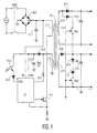
- Fig. 1 shows a schematic block diagram of a known switched-mode power supply using primary control.
- a diode rectifier bridge REC is connected to a line voltage source through a master switch SWM.
- An output from the rectifier bridge REC is connected to ground through a capacitor C11 and to one end of a primary winding L11 of a transformer TR.
- the other end of primary winding L11 is connected to one terminal of a controllable switch Tr11, the other terminal of which being connected to ground through a sense resistor R SENSE .
- a first secondary winding L12 of the transformer TR has a first end and a second end connected to each other through a series arrangement of a diode D11 and a main output capacitor C12, the second end of the first secondary winding L12 also being connected to ground.
- a load (not shown) may be connected across the main output capacitor C12.
- the transformer TR also includes a second secondary winding L13 having a first end and a second end connected to each other through a series arrangement of a diode D12 and a control output capacitor C13, the second end of the second secondary winding L13 also being connected to ground.
- a microprocessor (not shown), for controlling, for example, a television receiver in which the switched-mode power supply circuit is installed, is connected across the control output capacitor C13 to receive operating power.
- the first end of the first secondary winding L12 is also connected, via a diode D13 and a controllable switch Sw1, to one end of the control output capacitor C13, while the control output capacitor C13 is shunted by a series arrangement of a light emitting diode D14 of an opto-coupler, a Zener diode Z1 and a controllable switch Sw2.
- the controllable switches Sw1 and Sw2 are controlled by a signal from the microprocessor to initiate the stand-by mode of the switched-mode power supply circuit.
- the transformer TR further includes an auxiliary primary winding L14 which has one end connected to a diode D15, and then to ground through a V AUX capacitor C14, to a V AUX input of a controller IC, and to one terminal of a light sensor Tr12 of the opto-coupler, the other terminal of the light sensor Tr12 being connected to a stand-by mode detecting input (OOB)of the controller IC.
- the other end of the auxiliary primary winding L14 is connected to ground.
- the controller IC also has a V IN input connected to the output of the rectifier bridge REC, a DEMAG input connected through a resistor R11 to the one end of the auxiliary primary winding L14, a driver output connected to the control input of controllable switch Tr11, and an I SENSE input connected to the resistor R SENSE .
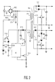
- Fig. 2 shows the switched-mode power supply circuit of Fig. 1 in which the subject invention has been incorporated.
- the series arrangement of two resistors R12 and R13 and a Zener diode Z2 is connected between the first output terminal of the rectifier bridge REC and ground.
- the junction between the Zener diode Z2 and resistor R13 is connected to the OOB input of the controller IC via a switch Sw3, which is further connected to ground via a resistor R14.
- switch Sw3 When it is desired to turn off the switched-mode power supply circuit, switch Sw3 is opened, removing the voltage across the Zener diode Z2 from the OOB input of the controller IC.
- the controller IC detects this drop in the voltage on the OOB input and stops the controllable switch Tr11 from switching. In this state, the controller IC draws less than 300 ⁇ A thereby effecting the OFF state.
- FIG. 2 uses a separate opto-coupler in primary sensing to signal the controller IC that burst mode stand-by is desired.
- an opto-coupler is already being used to regulate the control voltage during normal operation.
- FIG. 3 shows a second embodiment of the switched-mode power supply circuit of the subject invention in which the already existing opto-coupler is additionally used in secondary sensing to signal burst mode stand-by operation.
- the light emitting diode D14 of the opto-coupler is connected through resistors R15 and R16 to the anode of a Zener diode Z3, the cathode of which being connected to ground.
- a series combination of a resistor R17 and a capacitor C15 connects the anode of the Zener diode Z3 to a control terminal of the Zener diode Z3 and to junction point between resistors R18 and R19 connected between the output of the first secondary winding L12 and ground.
- Switch Sw2 connects the anode of Zener diode Z1 to the output of the second secondary winding L13, the cathode of Zener diode Z1 being connected to ground through the series arrangement of resistors R20 and R21.
- the junction between resistors R15 and R16 is connected to the collector of an NPN transistor Tr13, having an emitter connected to ground and a base connected to the junction between resistors R20 and R21.
- the junction between the light sensor Tr12 of the opto-coupler and the diode D16 is further connected through a resistor R22 to a V CNTL input of the controller IC which is also connected to ground through the parallel arrangement of a resistor R23 and a capacitor C16.
- transistor Tr13 is off and the intensity of the light being emitted by the light emitting diode D14 of the opto-coupler is controlled by the circuit R16-R19, C15 and Z3.
- This variable light intensity causes a corresponding response in the light sensor Tr12 which applies a portion of the V AUX voltage to the V CNTL input of the controller IC for regulating the controllable switch Tr11.
- transistor Tr13 turns on fully causing the light emitting diode D14 to emit a much increased light output, which, in turn, causes the light sensor Tr12 to apply the whole of the V AUX voltage to the OOB input of the controller IC.
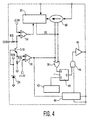
- the controller IC includes a start-up current source 30 coupled to the V IN input and a Vcc management circuit 32 connected to the V AUX input.
- the OOB input is connected to a resistor R24 and then to a first comparator 34 for comparing the voltage thereon to +2.4V, and generating an "OFF/ON" signal. This OFF/ON signal is applied to an input of the Vcc management circuit 32.
- the resistor R24 is also connected to the collector of an PNP transistor Tr15.
- the base of transistor Tr15 is connected to a Vcca voltage source, and to ground via a Zener diode 24.
- the emitter of the transistor Tr15 is connected to a second comparator 36 for comparing the voltage thereon to +1.4V, for generating a "Burst Mode Stand-by" signal S6.
- This signal S6 is applied to the start-up current source 30 and to one input of an OR-gate 38.
- An output (S5) from the Vcc management circuit 32 is also applied to the start-up current source 30 and to an inverting input of OR-gate 38.
- An output from OR-gate 38 is applied to the reset input of an RS flip-flop 40, the set input being connected to an output of an oscillator 42.
- the Q output from the RS flip-flop 40 is connected to one input of an AND-gate 44 which has an output connected to a driver 46 for driving the controllable switch Tr11.
- the Vcc management circuit 32 turns on the signal S5 and the controller IC (at t 2 ⁇ t ⁇ t 4 ) now starts causing the controllable switch Tr11 to switch which then causes the transformer TR to start transferring energy from the primary winding L11 to the secondary windings L12 and L13, and also to the auxiliary primary winding L14 which then takes over supplying the V AUX capacitor C14.
- the switched-mode power supply circuit is now in normal operation.
- the microprocessor closes switches Sw1 and Sw2 thereby coupling the first secondary winding L12 to the second secondary winding L13 thereby removing energy from the main output capacitor C12.
- switch Sw2 connects the light emitting diode D14 of the opto-coupler and the Zener diode Z1 across the second secondary winding L13.
- the coupling of the first and second secondary windings L12 and L13 now causes an increase in the control output voltage across the control output capacitor C13.
- the control output voltage exceeds the Zener diode Z1 voltage
- the light emitting diode D14 is energized. This causes the light sensor Tr12 to couple the V AUX voltage to the OOB input of the controller IC. Since the V AUX voltage is in excess of, for example, +5.6V, the comparator 36 generates the signal S6 resetting the flip-flop 40 which stops the controllable switch Tr11 from switching.
- transformer TR ceases transferring energy form the primary winding L11 to the first and second secondary windings L12 and L13 and to the auxiliary primary winding L14.
- the control output capacitor C13 and the V AUX capacitor C14 begin to drain causing the control voltage and the V AUX voltage to begin to drop.
- the light emitting diode D14 stops emitting light
- the light sensor Tr12 removes the V AUX voltage from input OOB of the controller IC, and the comparator 36 stops generating the signal S6.
- the Vcc management circuit 32 stops generating the signal S5 thereby maintaining the reset condition of the flip-flop 40, and activating the start-up current source 30 for charging up the V AUX capacitor C14 thereby raising the V AUX voltage.
- the Vcc management circuit 32 generates the S5 signal which turns off the start-up current source 30 and allows the controllable switch Tr11 to commence switching.
- the switching of the controllable switch Tr11 allows the transformer TR to transfer energy from the primary winding L11 to the first and second secondary windings L12 and L13 and to the auxiliary primary winding L14. This cycle then repeats itself until the microprocessor opens switches Sw1 and Sw2 indicating an end to the burst mode stand-by operation and a return to normal operation.
- resistors R14, R24 and R25, and transistor Tr15 provide this protection.
- resistor R14 ensures that the voltage at the OOB input is close to ground.
- the first comparator 34 then senses an OFF state and the controller IC goes into a "sleep" mode where it does not start the switched-mode power supply circuit.
- Burst mode is initiated by the light sensor Tr12 of the opto-coupler.
- the light sensor Tr12 forces a voltage greater than +5.6V at the OOB input and at the same time, provides a current large enough to force a voltage greater than the reference voltage, i.e., +1.4V, of the second comparator 36 on the resistor R25.
- the output of second comparator 36 then goes high and causes the switched-mode power supply circuit to go into burst mode stand-by operation.
- Resistor R24 is chosen based on a fault condition where the input OOB is shorted to the V AUX input. In such a situation, the system should then go into burst mode operation thereby keeping the dissipation in the switched-mode power supply circuit below 15W. To this end, R24 acts as a current limiter.
- Transistor Tr15 is chosen to be a bipolar PNP transistor, instead of a PMOS type transistor, because of the high threshold voltage of a PMOS transistor (2.1V). Due to this higher threshold voltage, the burst mode trip level would be raised. The higher trip level would then make it impossible to put the switched-mode power supply into burst mode stand-by operation when a fault occurred.
- V AUX When there is a short circuit between the OOB input and the V AUX input, the voltage V AUX is applied to the OOB input causing the second comparator 36 to detect burst mode stand-by operation.
- the voltage V CLAMP has a dependence on the value of R24, I START from the start-up current source 30, and temperature.
- the V AUX voltage can get clamped at a voltage which is lower than the start-up voltage for the controller IC. In such a state, the controller IC "hangs" and never initiates a start-up. If V CLAMP is higher than the start-up voltage, the controller IC starts up and immediately senses a burst mode condition.
Landscapes
- Engineering & Computer Science (AREA)
- Power Engineering (AREA)
- Dc-Dc Converters (AREA)
- Television Receiver Circuits (AREA)
Claims (8)
- Schaltnetzteil mit einer Betriebsmode und einer Bereitschaftsmode, wobei dieser Schaltnetzteil die nachfolgenden Elemente umfasst:Mittel (REC) zum Erzeugen einer DC-Speisespannung mit einer ersten Ausgangsklemme und einer zweiten Ausgangsklemme;einen Transformator (TR) mit einer Primärwicklung (L11), einer Hilfs-Primärwicklung (C14), und einer Sekundärwicklung (L12) mit einer ersten und einer zweiten Klemme, wobei von der genannten Primärwicklung (L11) eine erste Klemme mit der ersten Ausgangsklemme der genannten Speisespannungserzeugungsmittel (REC) gekoppelt ist, wobei die genannte Sekundärwicklung (L12) eine erste Ausgangsspannung in der Betriebsmode und eine zweite Ausgangsspannung in der Bereitschaftsmode schafft, wobei die genannte zweite Ausgangsspannung niedriger ist als die genannte erste Ausgangsspannung;einen steuerbaren Schalter (Tr11), der mit der zweiten Klemme der genannten Primärwicklung (L11) und der zweiten Ausgangsklemme der genannten Speisespannungserzeugungsmittel (REC) in Reihe verbunden ist;Mittel (SW1, D14, Tr12), die mit der genannten Sekundärwicklung (L12) gekoppelt sind zum Auslösen der genannten Bereitschaftsmode;einen Controller (IC) mit einem Ausgang zum Liefern von Schaltsignalen zu dem genannten steuerbaren Schalter (Tr11), einen Hilfsspannungsfühleingang, der über einen überbrückenden Hilfskondensator (C14) mit der genannten Hilfs-Primärwicklung (L14) des genannten Transformators (TR) gekoppelt ist, und mit einem Bereitschaftsmode-Detektiereingang (OOB), der mit einem Ausgang der genannten Bereitschaftsmode-Auslösemittel (SW1, D14, Tr12) gekoppelt ist, wobei der genannte Controller (IC) dafür sorgt, dass der genannte steuerbare Schalter (Tr11) während der genannten Breitschafismode intermittierend in Bursts schaltet, wobei der genannte Controller (IC) eine Aufstartstromquelle (30) aufweist zum Aufladen des genannten Hilfskondensators (C14) während des Aufstartens des genannten Schaltnetzteils, dadurch gekennzeichnet, dass während der genannten Bereitschaftsmode die genannte Aufstartstromquelle (30) benutzt wird zum intermittierenden Aufladen des Hilfskondensators (C14), wenn der genannte steuerbare Schalter (Tr11) nicht schaltet; undMittel (SW3) zum selektiven Koppeln des genannten Bereitschaftsmode-Detektiereingangs (OOB) des genannten Controllers mit der genannten ersten Ausgangsklemme der genannten Speisespannungserzeugungsmittel (REC), wobei der genannte Controller (IC) weiterhin Mittel (36) aufweist zum Abschalten der genannten Aufstartstromquelle (30) und Mittel (38, 40) zum Beenden der genannten Schaltsignale, wodurch der genannte Schaltnetzteil abgeschaltet wird, wenn die genannte erste Ausgangsklemme nicht mit dem genannten Bereitschaftsmodedetektionseingang (OOB) gekoppelt ist.
- Schaltnetzteil nach Anspruch 1, dadurch gekennzeichnet, dass in dem genannten Controller (IC) die genannten Abschaltmittel (36) eine Vergleichsschaltung (36) umfassen, von denen ein erster Eingang mit dem genannten Bereitschaftsmodedetektionseingang gekoppelt ist, wobei ein zweiter Eingang eine vorbestimmte Spannung (1,4 V) empfängt und von dem ein Ausgang mit einem Steuereingang der genannten Aufstartstromquelle (3) sowie mit Mitteln zum Beenden (38, 40) der genannten Schaltsignale gekoppelt ist, wodurch wenn eine Spannung an dem genannten Bereitschaftsmodedetektionseingang bis unter die genannte vorbestimmte Spannung abfällt, angegeben wird, dass die genannte erste Ausgangsklemme nicht mit dem genannten Bereitschaftsmodedetektionseingang gekoppelt ist, wobei die genannte Vergleichsschaltung (36) die genannten Aufstartstrommittel (30) abschaltet und dafür sorgt, dass die Mittel (38, 40) mit der Erzeugung der genannten Schaltsignale aufhören.
- Schaltnetzteil nach Anspruch 1, dadurch gekennzeichnet, dass der genannte Schaltnetzteil weiterhin Mittel (Z2, R12, R13) umfasst zum Begrenzen einer Spannung an dem genannten Bereitschaftsmodedetektionseingang (OOB) des genannten Controllers (IC), wenn die genannte erste Ausgangsklemme der genannten Spannungserzeugungsmittel (REC) mit dem genannten Bereitschaftsdetektionseingang des genannten Controllers gekoppelt ist.
- Schaltnetzteil nach Anspruch 3, dadurch gekennzeichnet, dass die genannten Begrenzungsmittel eine Reihenschaltung aus einem Widerstand (R12, R13) und einer Zener-Diode (Z2) umfasst, die zwischen der ersten Ausgangsklemme der genannten Speisespannungserzeugungsmittel (REC) und Erde vorgesehen ist, wobei die genannten Kopplungsmittel (SW3) einen Knotenpunkt zwischen dem genannten Widerstand (R12, R13) und der genannten Zener-Diode (Z2) mit dem genannten Bereitschafismodedetektionseingang (OOB) des genannten Controllers (IC) selektiv koppeln.
- Schaltnetzteil nach Anspruch 3, dadurch gekennzeichnet, dass der genannte Schaltnetzteil weiterhin Mittel umfasst zum Abführen (R14) einer Spannung an dem genannten Bereitschaftsmodedetektionseingang (OOB) des genannten Controllers (IC), wenn der genannte Bereitschaftsmodedetektionseingang (OOB) nicht mit der genannten ersten Klemme der genannten Erzeugungsmittel (REC) gekoppelt ist.
- Schaltnetzteil nach Anspruch 5, dadurch gekennzeichnet, dass die genannten Abführungsmittel (R14) einen Widerstand (R14) aufweisen, der den genannten Bereitschaftsmodedetektionseingang (OOB) mit Erde koppelt.
- Schaltnetzteil nach Anspruch 2, dadurch gekennzeichnet, dass der genannte Controller (IC) weiterhin Mittel (R22) aufweist zum Begrenzen des Energieverbrauchs, wenn die genannten Kopplungsmittel (SW3) die erste Ausgangsklemme der genannten Speisespannungserzeugungsmittel (REC) von dem genannten Bereitschaftsdetektionseingang (OOB) des genannten Controllers (IC) selektiv entkoppeln.
- Schaltnetzteil nach Anspruch 7, wobei der genannte Controller (IC) eine weitere Vergeleichsschaltung (34) aufweist, von der ein erster Eingang mit dem Bereitschaftsmodedetektionseingang (OOB) des genannten Controllers (IC) gekoppelt ist, von der ein zweiter Eingang eine weitere vorbestimmte Spannung (2,4 V) empfängt, und von der ein Ausgang mit einem weiteren Steuereingang der genannten Aufstartstromquelle (30) sowie mit Mitteln (38, 40) zum Beenden der Lieferung von Schaltsignalen zu dem genannten steuerbaren Schalter (Tr11) gekoppelt ist, wodurch, wenn die genannte Spannung an dem genannten Bereitschaftsmodedetektionseingang (OOB) der genannten Bereitschaftsmodeauslösungsmittel (SW1, D14, Tr12) eine Schwellenspannung übersteigt, die genannte weitere Vergleichsschaltung (34) dadurch den Bereitschaftsburstbetrieb auslöst, dass dafür gesorgt wird, dass die genannten Mittel (38, 40) die genannten Schaltsignale abschalten und dass die genannte Aufstartstromquelle (30) den Hilfskondensator (C14) auflädt, dadurch gekennzeichnet, dass die genannten den Stromverbrauch begrenzenden Mittel einen Widerstand (R22) aufweisen, der zwischen dem genannten Bereitschaftsmodedetektionseingang (OOB) und dem ersten Eingang der genannten Vergleichsschaltung (34) vorgesehen ist; und einen NPN-Transistor (Tr14), dessen Kollektor mit dem ersten Eingang der genannten Vergleichsschaltung (34) verbunden ist, dessen Emitter mit dem ersten Eingang der genannten weiteren Vergleichsschaltung (36) verbunden ist, die über einen weiteren Widerstand (R23) ebenfalls mit Erde verbunden ist und dessen Basis mit einer Spannungsquelle (VCCA) sowie über eine Zener-Diode (Z4) mit Erde verbunden ist, wodurch der genannte Widerstand (R22) als Strombegrenzer wirksam ist und der genannte NPN-Transistor gewährleistet, dass die weitere Vergleichsschaltung (36) den genannten Schaltnetzteil in die Bereitschaftsmode bringt, wenn eine Spannung, höher als die genannte Schwellenspannung, dem Bereitschaftsmodedetektionseingang (OOB) des genannten Controllers (IC) zugeführt wird.
Applications Claiming Priority (3)
| Application Number | Priority Date | Filing Date | Title |
|---|---|---|---|
| US903774 | 1992-06-24 | ||
| US08/903,774 US5995384A (en) | 1997-07-31 | 1997-07-31 | Functional on/off switch for switched-mode power supply circuit with burst mode operation |
| PCT/IB1998/001137 WO1999007061A2 (en) | 1997-07-31 | 1998-07-27 | Functional on/off switch for switched-mode power supply circuit with burst mode operation |
Publications (2)
| Publication Number | Publication Date |
|---|---|
| EP0941573A1 EP0941573A1 (de) | 1999-09-15 |
| EP0941573B1 true EP0941573B1 (de) | 2002-04-24 |
Family
ID=25418048
Family Applications (1)
| Application Number | Title | Priority Date | Filing Date |
|---|---|---|---|
| EP98932458A Expired - Lifetime EP0941573B1 (de) | 1997-07-31 | 1998-07-27 | Ein-/aus-funktionsschalter für schaltnetzteil mit burst-mode-betrieb |
Country Status (5)
| Country | Link |
|---|---|
| US (1) | US5995384A (de) |
| EP (1) | EP0941573B1 (de) |
| JP (1) | JP4430746B2 (de) |
| DE (1) | DE69805052T2 (de) |
| WO (1) | WO1999007061A2 (de) |
Families Citing this family (65)
| Publication number | Priority date | Publication date | Assignee | Title |
|---|---|---|---|---|
| DE19757364A1 (de) * | 1997-12-22 | 1999-07-01 | Siemens Ag | Schaltungsanordnung und Verfahren zur Erzeugung einer konstanten Ausgangsspannung bei Umrichtern |
| DE19826152A1 (de) * | 1998-06-12 | 1999-12-16 | Thomson Brandt Gmbh | Anordnung mit einem Schaltnetzteil und einem Mikroprozessor |
| US6292233B1 (en) * | 1998-12-31 | 2001-09-18 | Stmicroelectronics S.R.L. | Device controller with low power standby mode |
| US6137696A (en) * | 1999-04-12 | 2000-10-24 | Semicondutor Components Industries, Llc | Switching regulator for power converter with dual mode feedback input and method thereof |
| DE19932711A1 (de) * | 1999-07-16 | 2001-01-18 | Thomson Brandt Gmbh | Schaltnetzteil |
| JP4355058B2 (ja) * | 1999-07-27 | 2009-10-28 | 日本信号株式会社 | 電源装置 |
| US6462971B1 (en) | 1999-09-24 | 2002-10-08 | Power Integrations, Inc. | Method and apparatus providing a multi-function terminal for a power supply controller |
| US6462437B1 (en) * | 1999-11-12 | 2002-10-08 | Koninklijke Philips Electronics N.V. | System and method for alternating standby mode |
| US6344981B1 (en) * | 1999-11-16 | 2002-02-05 | Exabyte Corporation | Power supply circuit and method of calibration therefor |
| EP1124315B1 (de) * | 2000-02-11 | 2007-01-03 | Semiconductor Components Industries, LLC | Schaltnetzteil mit programmierbarem Impulsunterdrückungsmodus |
| JP3475892B2 (ja) * | 2000-02-25 | 2003-12-10 | 株式会社村田製作所 | スイッチング電源装置 |
| JP4606561B2 (ja) * | 2000-10-18 | 2011-01-05 | ローム株式会社 | インターフェース回路 |
| EP1209793A1 (de) * | 2000-11-23 | 2002-05-29 | Semiconductor Components Industries LLC | Verfahren und Gerät zur Steuerung einer Stromversorgungseinrichtung |
| US6480401B2 (en) * | 2001-03-13 | 2002-11-12 | Astec International Limited | Method and apparatus for reducing standby power in power supplies |
| KR100419224B1 (ko) * | 2002-01-19 | 2004-02-21 | 삼성전자주식회사 | 전원 절약 모드 기능을 갖는 전원 장치 |
| US6683443B2 (en) * | 2002-02-20 | 2004-01-27 | Texas Instruments Incorporated | Soft start circuit for regulated power supply |
| JP3697218B2 (ja) * | 2002-03-20 | 2005-09-21 | キヤノン株式会社 | 電源装置 |
| US6724174B1 (en) * | 2002-09-12 | 2004-04-20 | Linear Technology Corp. | Adjustable minimum peak inductor current level for burst mode in current-mode DC-DC regulators |
| KR101066996B1 (ko) * | 2002-10-29 | 2011-09-22 | 페어차일드코리아반도체 주식회사 | 펄스 폭 변조 신호 발생 장치 및 이를 포함하는 스위칭모드 파워 서플라이 |
| US7054170B2 (en) * | 2004-01-05 | 2006-05-30 | System General Corp. | Power-mode controlled power converter |
| CN2692915Y (zh) * | 2004-02-19 | 2005-04-13 | Bcd半导体制造有限公司 | 基于384x的跳频式pwm控制器 |
| KR101058935B1 (ko) * | 2004-05-03 | 2011-08-23 | 페어차일드코리아반도체 주식회사 | 스위칭 모드 파워 서플라이 |
| GB0410837D0 (en) * | 2004-05-14 | 2004-06-16 | Goodrich Control Sys Ltd | Compensation circuit and drive circuit including such a compensation circuit |
| US7071742B2 (en) * | 2004-06-15 | 2006-07-04 | Elster Electricity, Llc | Power supply restart delay prevention circuit |
| US7535735B2 (en) * | 2004-09-13 | 2009-05-19 | Power Integrations, Inc. | Compensation for parameter variations in a feedback circuit |
| CN101218737A (zh) * | 2005-05-10 | 2008-07-09 | Nxp股份有限公司 | 用于开关模式电源的反馈通信技术 |
| EP1732317A1 (de) * | 2005-06-07 | 2006-12-13 | TTE Germany GmbH | Stromversorgungsanordnung |
| US7529105B1 (en) * | 2006-11-03 | 2009-05-05 | Fairchild Semiconductor Corporation | Configuring a power converter to operate with or without burst mode functionality |
| US8013474B2 (en) | 2006-11-27 | 2011-09-06 | Xslent Energy Technologies, Llc | System and apparatuses with multiple power extractors coupled to different power sources |
| US9431828B2 (en) | 2006-11-27 | 2016-08-30 | Xslent Energy Technologies | Multi-source, multi-load systems with a power extractor |
| US7960870B2 (en) | 2006-11-27 | 2011-06-14 | Xslent Energy Technologies, Llc | Power extractor for impedance matching |
| US7839025B2 (en) | 2006-11-27 | 2010-11-23 | Xslent Energy Technologies, Llc | Power extractor detecting a power change |
| EP2238675A1 (de) * | 2007-12-31 | 2010-10-13 | Arçelik Anonim Sirketi | Stromversorgung |
| US8054656B2 (en) * | 2008-04-11 | 2011-11-08 | System General Corp. | Switching control circuit for a switching power converter |
| WO2009140404A2 (en) * | 2008-05-13 | 2009-11-19 | Igo , Inc. | Circuit and method for ultra-low idle power |
| US7770039B2 (en) * | 2008-05-29 | 2010-08-03 | iGo, Inc | Primary side control circuit and method for ultra-low idle power operation |
| US7779278B2 (en) * | 2008-05-29 | 2010-08-17 | Igo, Inc. | Primary side control circuit and method for ultra-low idle power operation |
| US7795759B2 (en) * | 2008-06-27 | 2010-09-14 | iGo, Inc | Load condition controlled power strip |
| US7795760B2 (en) * | 2008-07-25 | 2010-09-14 | Igo, Inc. | Load condition controlled power module |
| US7800252B2 (en) * | 2008-06-27 | 2010-09-21 | Igo, Inc. | Load condition controlled wall plate outlet system |
| WO2010019691A1 (en) * | 2008-08-12 | 2010-02-18 | Ixys Corporation | System and method for conserving power applied to an electrical apparatus |
| JP5268615B2 (ja) | 2008-12-15 | 2013-08-21 | キヤノン株式会社 | 電源装置および画像形成装置 |
| US8179699B2 (en) * | 2008-12-31 | 2012-05-15 | Stmicroelectronics S.R.L. | Method for controlling a switching regulator and related switching regulator |
| US8693228B2 (en) | 2009-02-19 | 2014-04-08 | Stefan Matan | Power transfer management for local power sources of a grid-tied load |
| TWI401556B (zh) * | 2009-04-10 | 2013-07-11 | Hon Hai Prec Ind Co Ltd | 電源模組 |
| US8698474B2 (en) * | 2010-06-11 | 2014-04-15 | System General Corp. | Start-up circuit with low standby power loss for power converters |
| KR101184252B1 (ko) | 2010-12-09 | 2012-09-21 | 박완수 | 대기전력 절감 smps |
| US9306460B2 (en) * | 2011-02-23 | 2016-04-05 | Vkr Holding A/S | Power supply comprising a standby feature |
| TWI582575B (zh) * | 2011-03-17 | 2017-05-11 | 和碩聯合科技股份有限公司 | 電子裝置 |
| KR101208182B1 (ko) | 2011-06-01 | 2012-12-04 | 삼성전기주식회사 | 전원공급장치, 전원공급장치의 제어 집적회로 및 전원공급장치의 제어방법 |
| MY165232A (en) * | 2012-02-10 | 2018-03-14 | Thomson Licensing | Switch mode power supply module and associated hiccup control method |
| US9036369B2 (en) * | 2012-10-12 | 2015-05-19 | Power Integrations, Inc. | Programming of an integrated circuit on a multi-function terminal |
| US9368961B2 (en) * | 2013-01-08 | 2016-06-14 | Power Integrations, Inc. | Overvoltage protection circuit |
| US9774266B2 (en) * | 2014-09-27 | 2017-09-26 | Apple Inc. | Reducing output voltage undershoot in isolated power converters |
| US9559597B2 (en) * | 2015-02-27 | 2017-01-31 | Dialog Semiconductor Inc. | Detecting open connection of auxiliary winding in a switching mode power supply |
| KR102384205B1 (ko) * | 2015-04-29 | 2022-04-07 | 삼성전자주식회사 | 전원 공급 장치 및 그의 전원 공급 방법 |
| CN105244981B (zh) * | 2015-11-20 | 2017-12-26 | 深圳市祝你快乐科技有限公司 | 一种能自动断电的节能充电器 |
| CN107743678B (zh) * | 2015-12-09 | 2019-12-31 | 富士电机株式会社 | 电力变换装置 |
| US10153702B2 (en) * | 2017-02-07 | 2018-12-11 | Infineon Technologies Austria Ag | Switched-mode power supply controller using a single pin for both input voltage sensing and control of power supply charging |
| EP3756262B1 (de) * | 2018-02-22 | 2024-01-10 | Volvo Truck Corporation | Mehrspannungsladevorrichtung |
| CN109194964A (zh) * | 2018-10-30 | 2019-01-11 | 北京优博信科技有限公司 | 一种安防视频压缩用设备 |
| TWI762896B (zh) * | 2020-04-01 | 2022-05-01 | 宏碁股份有限公司 | 消除過電流保護誤動作之電源供應器 |
| CN113839566B (zh) * | 2020-06-24 | 2023-07-21 | 宏碁股份有限公司 | 消除过电流保护误动作的电源供应器 |
| TWI726758B (zh) * | 2020-07-01 | 2021-05-01 | 宏碁股份有限公司 | 消除振鈴效應之電源供應器 |
| US12489370B2 (en) * | 2023-06-19 | 2025-12-02 | Power Forest Technology Corporation | Low power consumption feedback circuit for power supply device |
Family Cites Families (4)
| Publication number | Priority date | Publication date | Assignee | Title |
|---|---|---|---|---|
| NL8502338A (nl) * | 1985-08-26 | 1987-03-16 | Philips Nv | Geschakelde voedingsspanningsschakeling met twee toestanden. |
| KR100411170B1 (ko) * | 1995-04-05 | 2004-03-30 | 코닌클리케 필립스 일렉트로닉스 엔.브이. | 스위치모드전원공급회로및이를포함한화상디스플레이장치 |
| DE19518863A1 (de) * | 1995-05-23 | 1996-11-28 | Thomson Brandt Gmbh | Schaltnetzteil mit Bereitschaftsbetrieb |
| US5812383A (en) * | 1997-07-31 | 1998-09-22 | Philips Electronics North North America Corporation | Low power stand-by for switched-mode power supply circuit with burst mode operation |
-
1997
- 1997-07-31 US US08/903,774 patent/US5995384A/en not_active Expired - Lifetime
-
1998
- 1998-07-27 DE DE69805052T patent/DE69805052T2/de not_active Expired - Fee Related
- 1998-07-27 EP EP98932458A patent/EP0941573B1/de not_active Expired - Lifetime
- 1998-07-27 JP JP51072299A patent/JP4430746B2/ja not_active Expired - Lifetime
- 1998-07-27 WO PCT/IB1998/001137 patent/WO1999007061A2/en not_active Ceased
Also Published As
| Publication number | Publication date |
|---|---|
| DE69805052D1 (de) | 2002-05-29 |
| US5995384A (en) | 1999-11-30 |
| JP4430746B2 (ja) | 2010-03-10 |
| DE69805052T2 (de) | 2002-12-19 |
| EP0941573A1 (de) | 1999-09-15 |
| WO1999007061A2 (en) | 1999-02-11 |
| WO1999007061A3 (en) | 1999-04-29 |
| JP2001501439A (ja) | 2001-01-30 |
Similar Documents
| Publication | Publication Date | Title |
|---|---|---|
| US5995384A (en) | Functional on/off switch for switched-mode power supply circuit with burst mode operation | |
| EP0935843B1 (de) | Burst-mode-bereitschaftsbetrieb mit niedrigem energieverbrauch für schaltnetzteil | |
| US5852550A (en) | Switched-mode power supply circuit having a very low power stand-by mode | |
| EP0651310B1 (de) | Stromversorgungsvorrichtung | |
| JP3367300B2 (ja) | スイッチング電源回路 | |
| JPH0624390U (ja) | 電源回路 | |
| JP2001516520A (ja) | ビデオ表示装置用待機電源 | |
| JP3880071B2 (ja) | 電源 | |
| EP0914705A2 (de) | Auf einem entmagnetisierungssignal basierte überspannungsschutzschaltung für ein schaltnetzteil | |
| JP2784136B2 (ja) | スイッチング電源の過負荷・短絡保護回路 | |
| EP0794607B1 (de) | Schaltnetzteil | |
| JP4163959B2 (ja) | 電力コンバータに対する初期バイアス及びイネーブル信号を供給するための方法及び装置 | |
| JP2002204572A (ja) | スイッチング電源及びその制御方法 | |
| EP0806076B1 (de) | Stromversorgungsschaltung | |
| US6119238A (en) | Apparatus for generating a power off/on signal | |
| JP4292851B2 (ja) | 直流電源装置 | |
| JPH09113546A (ja) | 過電流検出回路 | |
| JP2673966B2 (ja) | バッテリ充電器 | |
| JP4374714B2 (ja) | スイッチング電源装置 | |
| JP3042171B2 (ja) | スイッチング電源装置 | |
| US6160356A (en) | Strobo system used for camera | |
| JPH06233528A (ja) | スイッチング電源装置 | |
| JP2705303B2 (ja) | 電源回路 | |
| JP2002135967A (ja) | 安定化電源における過電圧保護回路 | |
| JP2953941B2 (ja) | 電源起動切断回路 |
Legal Events
| Date | Code | Title | Description |
|---|---|---|---|
| PUAI | Public reference made under article 153(3) epc to a published international application that has entered the european phase |
Free format text: ORIGINAL CODE: 0009012 |
|
| 17P | Request for examination filed |
Effective date: 19990503 |
|
| AK | Designated contracting states |
Kind code of ref document: A1 Designated state(s): DE FR GB |
|
| 17Q | First examination report despatched |
Effective date: 20000508 |
|
| GRAG | Despatch of communication of intention to grant |
Free format text: ORIGINAL CODE: EPIDOS AGRA |
|
| GRAG | Despatch of communication of intention to grant |
Free format text: ORIGINAL CODE: EPIDOS AGRA |
|
| GRAH | Despatch of communication of intention to grant a patent |
Free format text: ORIGINAL CODE: EPIDOS IGRA |
|
| REG | Reference to a national code |
Ref country code: GB Ref legal event code: IF02 |
|
| GRAH | Despatch of communication of intention to grant a patent |
Free format text: ORIGINAL CODE: EPIDOS IGRA |
|
| GRAA | (expected) grant |
Free format text: ORIGINAL CODE: 0009210 |
|
| AK | Designated contracting states |
Kind code of ref document: B1 Designated state(s): DE FR GB |
|
| REG | Reference to a national code |
Ref country code: GB Ref legal event code: FG4D |
|
| REF | Corresponds to: |
Ref document number: 69805052 Country of ref document: DE Date of ref document: 20020529 |
|
| ET | Fr: translation filed | ||
| ET | Fr: translation filed | ||
| REG | Reference to a national code |
Ref country code: FR Ref legal event code: D6 |
|
| REG | Reference to a national code |
Ref country code: GB Ref legal event code: 746 Effective date: 20021205 |
|
| PLBE | No opposition filed within time limit |
Free format text: ORIGINAL CODE: 0009261 |
|
| STAA | Information on the status of an ep patent application or granted ep patent |
Free format text: STATUS: NO OPPOSITION FILED WITHIN TIME LIMIT |
|
| 26N | No opposition filed |
Effective date: 20030127 |
|
| REG | Reference to a national code |
Ref country code: GB Ref legal event code: 732E |
|
| REG | Reference to a national code |
Ref country code: FR Ref legal event code: TP |
|
| PGFP | Annual fee paid to national office [announced via postgrant information from national office to epo] |
Ref country code: DE Payment date: 20090723 Year of fee payment: 12 |
|
| REG | Reference to a national code |
Ref country code: FR Ref legal event code: ST Effective date: 20110331 |
|
| PG25 | Lapsed in a contracting state [announced via postgrant information from national office to epo] |
Ref country code: DE Free format text: LAPSE BECAUSE OF NON-PAYMENT OF DUE FEES Effective date: 20110201 |
|
| REG | Reference to a national code |
Ref country code: DE Ref legal event code: R119 Ref document number: 69805052 Country of ref document: DE Effective date: 20110201 |
|
| PG25 | Lapsed in a contracting state [announced via postgrant information from national office to epo] |
Ref country code: FR Free format text: LAPSE BECAUSE OF NON-PAYMENT OF DUE FEES Effective date: 20100802 |
|
| PGFP | Annual fee paid to national office [announced via postgrant information from national office to epo] |
Ref country code: FR Payment date: 20090911 Year of fee payment: 12 |
|
| REG | Reference to a national code |
Ref country code: GB Ref legal event code: 732E Free format text: REGISTERED BETWEEN 20121108 AND 20121114 |
|
| PGFP | Annual fee paid to national office [announced via postgrant information from national office to epo] |
Ref country code: GB Payment date: 20170626 Year of fee payment: 20 |
|
| REG | Reference to a national code |
Ref country code: GB Ref legal event code: PE20 Expiry date: 20180726 |
|
| PG25 | Lapsed in a contracting state [announced via postgrant information from national office to epo] |
Ref country code: GB Free format text: LAPSE BECAUSE OF EXPIRATION OF PROTECTION Effective date: 20180726 |