EP0938812B1 - Standby power supply for video display apparatus - Google Patents
Standby power supply for video display apparatus Download PDFInfo
- Publication number
- EP0938812B1 EP0938812B1 EP97911395A EP97911395A EP0938812B1 EP 0938812 B1 EP0938812 B1 EP 0938812B1 EP 97911395 A EP97911395 A EP 97911395A EP 97911395 A EP97911395 A EP 97911395A EP 0938812 B1 EP0938812 B1 EP 0938812B1
- Authority
- EP
- European Patent Office
- Prior art keywords
- standby
- run
- mode
- power supply
- switch
- Prior art date
- Legal status (The legal status is an assumption and is not a legal conclusion. Google has not performed a legal analysis and makes no representation as to the accuracy of the status listed.)
- Expired - Lifetime
Links
- 238000004804 winding Methods 0.000 claims description 55
- 230000008878 coupling Effects 0.000 claims description 4
- 238000010168 coupling process Methods 0.000 claims description 4
- 238000005859 coupling reaction Methods 0.000 claims description 4
- 239000003990 capacitor Substances 0.000 description 11
- 230000005669 field effect Effects 0.000 description 5
- 230000009977 dual effect Effects 0.000 description 4
- 238000010586 diagram Methods 0.000 description 2
- 230000001105 regulatory effect Effects 0.000 description 2
- 229920002799 BoPET Polymers 0.000 description 1
- RYGMFSIKBFXOCR-UHFFFAOYSA-N Copper Chemical compound [Cu] RYGMFSIKBFXOCR-UHFFFAOYSA-N 0.000 description 1
- 239000004677 Nylon Substances 0.000 description 1
- 230000006378 damage Effects 0.000 description 1
- 230000001419 dependent effect Effects 0.000 description 1
- 238000009413 insulation Methods 0.000 description 1
- 238000002955 isolation Methods 0.000 description 1
- 238000012986 modification Methods 0.000 description 1
- 230000004048 modification Effects 0.000 description 1
- 229920001778 nylon Polymers 0.000 description 1
- 230000002747 voluntary effect Effects 0.000 description 1
Images

Classifications
-
- H—ELECTRICITY
- H04—ELECTRIC COMMUNICATION TECHNIQUE
- H04N—PICTORIAL COMMUNICATION, e.g. TELEVISION
- H04N5/00—Details of television systems
- H04N5/63—Generation or supply of power specially adapted for television receivers
-
- H—ELECTRICITY
- H02—GENERATION; CONVERSION OR DISTRIBUTION OF ELECTRIC POWER
- H02J—CIRCUIT ARRANGEMENTS OR SYSTEMS FOR SUPPLYING OR DISTRIBUTING ELECTRIC POWER; SYSTEMS FOR STORING ELECTRIC ENERGY
- H02J9/00—Circuit arrangements for emergency or stand-by power supply, e.g. for emergency lighting
- H02J9/005—Circuit arrangements for emergency or stand-by power supply, e.g. for emergency lighting using a power saving mode
-
- H—ELECTRICITY
- H02—GENERATION; CONVERSION OR DISTRIBUTION OF ELECTRIC POWER
- H02M—APPARATUS FOR CONVERSION BETWEEN AC AND AC, BETWEEN AC AND DC, OR BETWEEN DC AND DC, AND FOR USE WITH MAINS OR SIMILAR POWER SUPPLY SYSTEMS; CONVERSION OF DC OR AC INPUT POWER INTO SURGE OUTPUT POWER; CONTROL OR REGULATION THEREOF
- H02M3/00—Conversion of DC power input into DC power output
- H02M3/22—Conversion of DC power input into DC power output with intermediate conversion into AC
- H02M3/24—Conversion of DC power input into DC power output with intermediate conversion into AC by static converters
- H02M3/28—Conversion of DC power input into DC power output with intermediate conversion into AC by static converters using discharge tubes with control electrode or semiconductor devices with control electrode to produce the intermediate AC
- H02M3/285—Single converters with a plurality of output stages connected in parallel
-
- H—ELECTRICITY
- H02—GENERATION; CONVERSION OR DISTRIBUTION OF ELECTRIC POWER
- H02M—APPARATUS FOR CONVERSION BETWEEN AC AND AC, BETWEEN AC AND DC, OR BETWEEN DC AND DC, AND FOR USE WITH MAINS OR SIMILAR POWER SUPPLY SYSTEMS; CONVERSION OF DC OR AC INPUT POWER INTO SURGE OUTPUT POWER; CONTROL OR REGULATION THEREOF
- H02M1/00—Details of apparatus for conversion
- H02M1/0003—Details of control, feedback or regulation circuits
- H02M1/0032—Control circuits allowing low power mode operation, e.g. in standby mode
-
- Y—GENERAL TAGGING OF NEW TECHNOLOGICAL DEVELOPMENTS; GENERAL TAGGING OF CROSS-SECTIONAL TECHNOLOGIES SPANNING OVER SEVERAL SECTIONS OF THE IPC; TECHNICAL SUBJECTS COVERED BY FORMER USPC CROSS-REFERENCE ART COLLECTIONS [XRACs] AND DIGESTS
- Y02—TECHNOLOGIES OR APPLICATIONS FOR MITIGATION OR ADAPTATION AGAINST CLIMATE CHANGE
- Y02B—CLIMATE CHANGE MITIGATION TECHNOLOGIES RELATED TO BUILDINGS, e.g. HOUSING, HOUSE APPLIANCES OR RELATED END-USER APPLICATIONS
- Y02B70/00—Technologies for an efficient end-user side electric power management and consumption
- Y02B70/10—Technologies improving the efficiency by using switched-mode power supplies [SMPS], i.e. efficient power electronics conversion e.g. power factor correction or reduction of losses in power supplies or efficient standby modes
Definitions
- This invention relates generally to the field of power supplies, and, in particular, to standby mode power supplies for video display apparatus such as, for example, television receivers.
- the power consumption of a video display apparatus may approach, or even exceed, approximately ten watts during standby mode operation.
- a level of standby power consumption poses a concern.
- an article in the September 19, 1997, issue of Europe Energy reports that the European Commission regards reducing the energy consumed by electronic equipment in the standby mode of operation as a priority.
- the article further states that the Commission has concentrated its initial efforts at reducing the standby power consumption of televisions and VCRs, and that it has elicited voluntary commitments from manufacturers of such products to progressively reduce average standby power consumption to less than three watts.
- a conventional power supply arrangement for a video display apparatus is disclosed in Japanese laid-open patent document number JP 6-225529.
- a run mode output stage 2 is coupled to a converter 1 through a switch SW, and a standby mode output stage 3 is inseparably connected to the converter 1.
- the arrangement disclosed in JP 6-225529 is undesirably inefficient because the standby mode output stage 3 dissipates power during the run mode of operation.
- a single power supply circuit is used to implement both standby and run mode operation.
- the power supply control circuit senses that the secondary side of the power supply is unloaded, the power supply is placed into a "burst" mode of standby operation, whereby the power supply continues to generate standby voltages for the remote control receiver and the microcontroller.
- a disadvantage of this conventional power supply implementation in that the primary inductance of the switched mode power supply transformer is too law for proper standby operation. This low primary inductance results in uncreased power consumption by the video display apparatus in the standby mode.
- the reduction in the energy consumed by the video display apparatus during the standby mode of operation dictates either that the pulse width of the drive pulses from power supply control circuit be reduced ; or, that the inductance seen by the drive pulses during the standby mode be increased relative to the inductance of the primary winding of the switched mode power supply transformer.
- the present invention is directed to increase the inductance seen by the drive pulses of a power supply control circuit during the standby mode of operation and to further reduce power dissipation in both the run and standby modes.
- a switched mode power supply circuit is as defined in claim 1. It preferably comprises : a run mode output stage for providing a run mode output voltage during said run mode of operation ; a standby mode output stage for providing a standby mode output voltage during said standby mode of operation ; and a control circuit coupled to said run and standby mode output stages for providing drives pulses to only one of said output stages during each of said modes of operation.
- the dependent claims relate to embodiments thereof.
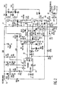
- a dual switched mode power supply circuit 100 shown in FIGURE 1 embodies an inventive arrangement for a standby mode power supply for a television receiver.
- the power supply circuit 100 uses two switched-mode power supplies: a run mode power supply using a flyback transformer T1 and a standby mode power supply using a flyback transformer T2.
- Run transformer T1 is used during the run mode operation of the television receiver.
- Run transformer T1 has a primary winding n1 which has a first terminal 11 coupled to the rectified mains voltage 10 and a second terminal 12 coupled to a run power switch Q1.
- the secondary winding n2 is coupled to the switched mode power supply controller circuit 20, and the secondary windings n3 and n4 provide voltages which, after being rectified by diodes D5 and D4, respectively, are used to power other circuits within the television receiver.
- the secondary winding n3 is used to power the microcontroller (not shown) and the remote control receiver (not shown) when the television receiver is in the run mode.
- the standby transformer T2 is used during the standby mode operation of the television receiver.
- Standby transformer T2 has a primary winding n51 which has a first terminal 14 coupled to the rectified mains voltage 10 and a second terminal 15 coupled to a standby power switch Q51.
- the secondary winding n52 is coupled to the switched mode power supply controller circuit 20, and a secondary winding n53 provides a standby voltage which, after being rectified by diode D57, is used to power the microcontroller and the remote control receiver when the television receiver operates in a standby mode.
- the run power switch Q1 and the standby power switch Q51 are both controlled by the switched mode power supply controller circuit 20.
- the first switch S1 is open and the second switch S2 is closed, as shown in FIGURE 1.
- the control electrode 13 of the power switch Q1 is coupled to the ground, or reference potential, and the power switch Q1 is thus turned off.
- the drive pulses 30 at the output of the switched mode power supply controller circuit 20 are coupled to the control electrode 16 of the standby power switch Q51 through the resistor R55.
- the standby power switch Q51 switches responsive to the drive pulses 30, energy is transferred from the primary winding n51 of the standby transformer T2 to the secondary winding n53.
- the voltage across the secondary winding n53 is rectified by the diode D57 to provide the voltage Vn3 to the microcontroller and the remote control receiver.
- the first switch S1 is closed and the second switch S2 is open.
- the control electrode 16 of the standby power switch Q51 1 is coupled to the ground, or reference, potential and the standby power switch Q51 is turned off.
- the drive pulses 30 at the output of the switched mode power supply controller circuit 20 are coupled to the control electrode 13 of the run power switch Q1 through the resistor R10.
- the run power switch Q1 switches responsive to drive pulses 30, energy is transferred from the primary winding n1 of the run transformer T1 to the secondary windings n3 and n4.
- the voltages across the secondary windings n3 and n4 are rectified by the diodes D5 and D4, respectively, to power other circuits within the television receiver.
- FIGURE 2 illustrates a presently preferred embodiment of the dual switched mode power supply circuit 100, which uses field effect transistors for the run power switch Q1 and the standby power switch Q51.
- the run transformer T1 may comprise a conventional design for switched-mode power supply applications, and will not be described further herein.
- the standby transformer T2 used in the preferred embodiment of FIGURE 2 was constructed using an E16 type core with a total air gap of 0.1 mm.
- the primary winding n51 has approximately 500 turns of 0.1 mm CuN wire (copper wire with nylon insulation).
- the secondary winding n52 has approximately 60 turns and the secondary winding n53 has approximately 24 turns. Approximately 5 layers of 0.1 mm thickness MYLAR® brand polymeric film provide electrical isolation between the primary winding n51 and the secondary windings n52 and n53.
- the inductance of the primary winding n51 is equal to approximately 70 mH, which is relatively large in comparison to the inductance of the primary winding n1 of the run transformer T1. This relatively high inductance is necessary to accommodate the use of the switched mode power supply controller circuit 20 with the standby transformer T2.
- the reduction in the energy consumed by the video display apparatus during the standby mode of operation dictates either that the pulse width of the drive pulses 30 from the switched mode power supply controller circuit 20 be reduced; or, that the inductance seen by the drive pulses 30 during the standby mode be increased relative to the inductance of the primary winding n1 of the run transformer T1.
- the relatively high inductance of the primary winding n51 of the standby transformer T2 is used because the drive pulses 30 from the switched mode power supply controller circuit 20 cannot have a pulse width that is smaller than a minimum pulse width.
- a typical minimum pulse width may equal, for example, approximately one microsecond. Due to the relatively high inductance of the primary winding n51 of the standby transformer T2, the drive pulses 30 have a substantially similar frequency and duty cycle regardless of whether they are applied to the run power switch Q1 in the run mode or to the standby power switch Q51 in the standby mode.
- the power supply circuit 100 has a separate feedback path for both the run and standby modes of operation of the television receiver.
- a voltage at the terminal 17 of the run transformer T1 is fed back to the switched mode power supply controller circuit 20.
- the switched mode power supply controller circuit 20 may comprise, for example, a TDA4605 power supply controller integrated circuit manufactured by Siemens Aktiengesellschaft.
- the following voltages are fed back from terminal 17 of the secondary winding n2 to the controller circuit 20: a supply voltage to pin 6 of the controller circuit 20 through the diode D1; a zero detector voltage to pin 8 of the controller circuit 20 through the resistors R8 and R9 and the capacitor C6; and a regulating voltage to pin 1 of the controller circuit 20 through the resistor R9, the capacitor C6, and the diode D2.
- a voltage at the terminal 18 of the standby transformer T2 is fed back to the switched mode power supply controller circuit 20.
- the following voltages are fed back from terminal 18 of the secondary winding n52 to the controller circuit 20: a supply voltage to pin 6 of the controller circuit 20 through the diode D51; a zero detector voltage to pin 8 of the controller circuit 20 through the resistors R52 and R53 and the capacitor C51; and a regulating voltage to pin 1 of the controller circuit 20 through the resistor R53, the capacitor C51, and the diode D52.
- the current I diode flowing through the light-emitting diode of the optocoupler 40 is equal to approximately zero.
- the transistor Q53 is thus off and the drive pulses 30 from pin 5 of the controller circuit 20 are applied to the control electrode 16, or gate electrode, of the standby power switch Q51.
- the drive pulses 30 turn on the standby power switch Q51, the base electrode of the drive transistor Q52 is coupled to the ground, or reference potential, through the diode D55 and the standby power switch Q51; the drive transistor Q52 and the run power switch Q1 are thereby turned off.
- the voltage at the drain electrode of the standby power switch Q51 can be used in this way to control the drive transistor Q52, and hence the run power switch Q1, because the standby power switch Q51 can switch more rapidly than the run power switch Q1.
- the current I diode flowing through the light-emitting diode of the optocoupler 40 is equal to approximately two milliamps.
- This turns on the transistor of the optocoupler 40, thereby coupling a supply voltage, equal to approximately +12 V in the preferred embodiment shown in FIGURE 2, to the base electrode of the transistor Q53 through the voltage divider formed by the resistors R57 and R58.
- the transistor Q53 thus turns on, thereby bringing the control electrode 16, or gate electrode, of the standby power switch Q51 to the ground, or reference, potential.
- the standby power switch Q51 thus turns off and the voltage at the drain electrode of the standby power switch 51 goes to a high level.
- the diode D55 becomes reverse biased and the drive pulses 30 are applied through the resistor R54 to the base electrode of the drive transistor Q52 and through the resistor R10 to the collector electrode of the drive transistor Q52.
- the drive transistor Q52 then drives the run power switch Q1 responsive to the drive pulses 30.
- energy is transferred from the primary winding n1 of the run transformer T1 to the secondary windings n3 and n4.
- the voltages across the secondary windings n3 and n4 are rectified by the diodes D5 and D4, respectively, to power other circuits within the television receiver.
- the anode of the diode D56 is coupled to the emitter electrode of the drive transistor Q52 and the cathode of the diode D56 is coupled to a terminal of the resistor R56.
- the other terminal of the resistor R56 is coupled to the base electrode of the transistor Q53.
- the diode D54 is coupled in parallel with, and oppositely poled to, the drive transistor Q52.
- the diode D54 and the resistor R10 which couples the output pin 5 of the controller circuit 20 to the collector electrode of the drive transistor 52, provide a path to discharge the gate capacitance of the run power switch Q1, thereby enabling the run power switch to turn off.
- the output capacitors for example the capacitor C8 in FIGURE 2
- the run power switch Q1 When the television receiver is switched from the standby mode to the run mode, the output capacitors, for example the capacitor C8 in FIGURE 2, are discharged.
- the run power switch Q1 When the run power switch Q1 then turns on for the first time in the run mode after the switch from the standby mode, an excessively high peak current may flow through the run power switch Q1, possibly destroying it.
- the excessively high current is a consequence of the feature of a flyback system that a relatively long time is required to transfer energy from a primary winding of a flyback transformer, for example primary winding n1 of run transformer T1, to a secondary side of the flyback transformer, for example secondary winding n4 of the run transformer T1, if the voltage at the secondary side of the flyback transformer is relatively low.
- a small current is fed to pin 1 of the controller circuit 20 through the resistor R51.
- the magnitude of the current is equal to approximately (+12 V / R51), which for the embodiment shown in FIGURE 2 is equal to approximately 26 ⁇ A.
- This current simulates a high feedback voltage at pin 1 of the controller circuit 20, which causes the controller circuit 20 to go into a "no-load” mode or a "burst” mode, whereby the pulse widths of the drive pulses 30 are reduced to their minimum width.
- the width of the drive pulses 30 increases and eventually returns to a nominal width as the output capacitors become charged.
- a snubber circuit 60 formed by the series combination of the capacitor C52 and the diode D53 is coupled in parallel with the primary winding n51 of the standby transformer T2.
- the snubber circuit 60 is used to control the current in the start-up resistor R1.
- a voltage Vs at the junction of the capacitor C52 and the diode D53 is greater than the rectified mains voltage at the emitter electrode of the start-up transistor Q54.
- the start-up transistor Q54 is thus off, no current flows through the start-up resistor R1 during the standby mode, and, consequently, the power consumption is reduced during the standby mode.
- the snubber network 61 for the primary winding n1 of the run transformer T1 could also be used to turn off the start-up transistor Q54, by coupling a junction of the capacitor C7 and the diode D3 to the start-up transistor through an appropriately valued resistance.
- FIGURE 3 shows a dual switched mode power supply circuit 100', which uses a bipolar junction transistor for the standby power switch Q51'.
- the standby power switch Q51 can be implemented using either a field effect or a bipolar junction transistor, as will be seen in FIGURES 2 and 3.
- the run power switch Q1 can also be implemented using a bipolar junction transistor. Using a bipolar junction transistor for the run power switch Q1 would require a different controller circuit 20, for example a TDA4601 power supply controller integrated circuit manufactured by Siemens Aktiengesellschaft; a drive circuit specific to bipolar junction transistors would also be required. Such modifications are well within the purview of one having ordinary skill in the art.
- the embodiment shown in FIGURE 3 operates substantiality in the same manner as the embodiment shown in FIGURE 2.
- One difference between field effect and bipolar junction transistors is that the turn-on time of a bipolar transistor is longer than that for a field effect transistor. Therefore, unlike in the embodiment shown in FIGURE 2, wherein the voltage at the drain electrode of the standby power switch Q51 was used to control the drive transistor Q52 and hence the run power switch Q1, the voltage at the collector electrode of the standby power switch Q51' cannot be used to control the drive transistor Q52.
- the drive transistor Q52 is controlled by the optocoupler 40 through the transistor Q55.
- the drive circuit for the standby power switch Q51 comprises the resistors R55 and R61, the capacitor C53, and the diodes D59 and60 ; the operation of this drive circuit is well-known to those having ordinary skill in the art and will not be described further herein.
- the transistor of the optocoupler 40 does not conduct, so that the transistor Q53 is off and the standby power switch Q51 is consequently switching responsive to the drive pulses 30 from the controller circuit 20.
- the transistor Q55 is on, so that both the drive transistor Q52 and the run power switch Q1 are off.
- the transistor of the optocoupler 40 conducts ; the transistor Q53 is on and the standby power switch Q51 is consequently off ; the transistor Q55 is off ; and the drive transistor Q52 drives the run power switch Q1 responsive to the drive pulses 30 from the controller circuit 20.
- the present invention advantageously reduces the power consumed by a television receiver operating in the standby mode. For example, assuming a load equal to approximately 200 mW, which approximates a standard microcontroller operating in the run mode, the power consumed by the television receiver may be reduced from approximately six watts to approximately one watt by utilizing the inventive arrangement described herein.
Landscapes
- Engineering & Computer Science (AREA)
- Power Engineering (AREA)
- Multimedia (AREA)
- Signal Processing (AREA)
- Business, Economics & Management (AREA)
- Emergency Management (AREA)
- Dc-Dc Converters (AREA)
- Television Receiver Circuits (AREA)
Applications Claiming Priority (3)
| Application Number | Priority Date | Filing Date | Title |
|---|---|---|---|
| GBGB9623612.0A GB9623612D0 (en) | 1996-11-13 | 1996-11-13 | Separate power supplies for standby operation |
| GB9623612 | 1996-11-13 | ||
| PCT/IB1997/001431 WO1998021886A1 (en) | 1996-11-13 | 1997-11-13 | Standby power supply for video display apparatus |
Publications (2)
| Publication Number | Publication Date |
|---|---|
| EP0938812A1 EP0938812A1 (en) | 1999-09-01 |
| EP0938812B1 true EP0938812B1 (en) | 2003-02-12 |
Family
ID=10802871
Family Applications (1)
| Application Number | Title | Priority Date | Filing Date |
|---|---|---|---|
| EP97911395A Expired - Lifetime EP0938812B1 (en) | 1996-11-13 | 1997-11-13 | Standby power supply for video display apparatus |
Country Status (11)
| Country | Link |
|---|---|
| US (2) | US6144566A (enExample) |
| EP (1) | EP0938812B1 (enExample) |
| JP (2) | JP3809499B2 (enExample) |
| KR (2) | KR100497578B1 (enExample) |
| CN (2) | CN1202659C (enExample) |
| AU (2) | AU4880497A (enExample) |
| DE (2) | DE19782104T1 (enExample) |
| GB (1) | GB9623612D0 (enExample) |
| MY (1) | MY128192A (enExample) |
| TW (1) | TW391138B (enExample) |
| WO (2) | WO1998021886A1 (enExample) |
Families Citing this family (33)
| Publication number | Priority date | Publication date | Assignee | Title |
|---|---|---|---|---|
| HU225166B1 (en) | 1998-09-25 | 2006-07-28 | Koninkl Philips Electronics Nv | Signal processing apparatus having means for reducing the power consumption |
| JP2000299231A (ja) * | 1999-04-15 | 2000-10-24 | Fujitsu Ltd | トランス及びスイッチングレギュレータ |
| US6166926A (en) * | 2000-01-11 | 2000-12-26 | Thomson Licensing S.A. | Zero voltage switching power supply with burst mode |
| US6578152B1 (en) * | 2000-02-04 | 2003-06-10 | Iomega Corporation | Dual power switching network system for isolating between different power supplies and applying appropriate power supply to a connected peripheral device |
| US6324082B1 (en) | 2000-06-06 | 2001-11-27 | Thomson Licensing, S.A. | Mains frequency synchronous burst mode power supply |
| KR100376131B1 (ko) | 2000-09-22 | 2003-03-15 | 삼성전자주식회사 | 대기전원 절전형 전원장치 및 그 제어방법 |
| DE10106132A1 (de) * | 2001-02-10 | 2002-08-14 | Philips Corp Intellectual Pty | Aufwachschaltung für ein elektrisches Gerät |
| US6650028B1 (en) * | 2001-11-27 | 2003-11-18 | Verilink, Inc. | Dual isolated input power supply |
| KR100503207B1 (ko) * | 2002-03-11 | 2005-07-25 | 박춘식 | 전자파를 에너지원으로 사용하는 전자파 감소장치 |
| US7586548B2 (en) * | 2002-12-02 | 2009-09-08 | Sony Corporation | Stand-by power supply shutdown at power on |
| GB2402271B (en) | 2003-05-27 | 2006-04-19 | Research In Motion Ltd | Method and apparatus for handling a charging state in a mobile electronic device |
| EP2562618A3 (en) * | 2004-02-17 | 2013-05-22 | Research In Motion Limited | Method and apparatus for handling a charging state in a mobile electronic device |
| EP2808755B1 (en) * | 2004-02-17 | 2019-03-06 | Fundamental Innovation Systems International LLC | Method and apparatus for handling a charging state in a mobile electronic device |
| EP1771931B1 (en) * | 2004-07-23 | 2018-07-11 | Thomson Licensing DTV | A system and method for reducing standby power consumption |
| DE102005006175A1 (de) * | 2005-02-10 | 2006-08-24 | Siemens Ag Österreich | Schaltnetzteil mit vom Betriebszustand des Leistungsteils unabhängiger Versorgung von Einrichtungen |
| TWI316176B (en) * | 2005-05-06 | 2009-10-21 | Amtran Technology Co Ltd | Power switch circuit |
| US7414868B2 (en) * | 2005-06-20 | 2008-08-19 | Astec International Limited | Switched current power converter with partial converter decoupling for low load conditions |
| US20070001017A1 (en) * | 2005-06-29 | 2007-01-04 | Moshe Nuri | Reduced complexity multifunction expansion card and method of operating the same |
| US7586765B2 (en) * | 2005-07-26 | 2009-09-08 | Astec International Limited | Switched current power converter with reduced power losses during low load conditions |
| US20070085574A1 (en) * | 2005-10-11 | 2007-04-19 | Atron Lo | Audio signal detection utilizing low power standby power supply |
| US20070134063A1 (en) * | 2005-12-14 | 2007-06-14 | Shaw And Sons, Inc. | Dowel device with closed end speed cover |
| CN200976549Y (zh) * | 2006-09-22 | 2007-11-14 | 何曙光 | 一种超低功耗待机电路 |
| US20100164450A1 (en) * | 2008-12-30 | 2010-07-01 | International Business Machines Corporation | Apparatus, system, and method for providing high efficiency in a power supply over a range of load conditions |
| KR20110051862A (ko) * | 2009-11-11 | 2011-05-18 | 삼성전자주식회사 | 대기모드에서 hdmi를 통한 네트워크 통신장치 및 방법 |
| EP2372493B1 (en) | 2010-03-30 | 2020-05-13 | Electrolux Home Products Corporation N.V. | Device for reducing standby-mode energy consumption of an electric household appliance |
| EP2372488B1 (en) | 2010-03-30 | 2013-08-07 | Electrolux Home Products Corporation N.V. | Household appliance circuit arrangement |
| EP2434613B1 (en) | 2010-09-28 | 2018-02-21 | Electrolux Home Products Corporation N.V. | Electronic control device and method for reducing stand-by state energy consumption of an electric household appliance |
| EP2434612B1 (en) * | 2010-09-28 | 2020-09-09 | Electrolux Home Products Corporation N.V. | Electronic control device and method for reducing stand-by state energy consumption of an electric household appliance |
| CN104345659A (zh) * | 2013-08-06 | 2015-02-11 | 海尔集团公司 | 家电设备功能模块的电源控制方法和电路 |
| TWI503645B (zh) * | 2014-05-07 | 2015-10-11 | Nuvoton Technology Corp | 電壓調節器、方法與晶片 |
| CN105652718B (zh) * | 2016-02-29 | 2018-09-11 | 深圳市中兴环境仪器有限公司 | 一种水下小功率开关装置和开关系统 |
| CN106896859B (zh) * | 2017-04-06 | 2018-09-25 | 六安市同心畅能电子科技有限公司 | 一种全自动洗衣机零功耗待机电路 |
| CN110995009B (zh) * | 2019-12-18 | 2021-08-03 | 深圳航天科技创新研究院 | 一种一体化阴极电源及其系统 |
Family Cites Families (9)
| Publication number | Priority date | Publication date | Assignee | Title |
|---|---|---|---|---|
| DE3223756C2 (de) * | 1982-06-25 | 1984-08-23 | Licentia Patent-Verwaltungs-Gmbh, 6000 Frankfurt | Schaltnetzteil für ein elektrisches Gerät mit Bereitschaftsbetrieb, insbesondere einen Fernsehempfänger |
| US4751580A (en) * | 1985-12-19 | 1988-06-14 | Rca Licensing Corporation | Television receiver standby power supply |
| FR2607991B1 (fr) * | 1986-12-05 | 1989-02-03 | Radiotechnique Ind & Comm | Alimentation a decoupage pour un televiseur muni d'un systeme de veille |
| US4734771A (en) * | 1987-04-24 | 1988-03-29 | Rca Corporation | Start-up control circuitry for a television apparatus |
| GB9000238D0 (en) * | 1990-01-05 | 1990-03-07 | Rca Licensing Corp | Minimum power standby circuit arrangement |
| JPH06225529A (ja) * | 1993-01-21 | 1994-08-12 | Sony Corp | スイッチング電源装置 |
| EP0765541B1 (en) * | 1995-04-05 | 2000-08-09 | Koninklijke Philips Electronics N.V. | Switched-mode power supply |
| US5812383A (en) * | 1997-07-31 | 1998-09-22 | Philips Electronics North North America Corporation | Low power stand-by for switched-mode power supply circuit with burst mode operation |
| US5852550A (en) * | 1997-08-04 | 1998-12-22 | Philips Electronics North America Corporation | Switched-mode power supply circuit having a very low power stand-by mode |
-
1996
- 1996-11-13 GB GBGB9623612.0A patent/GB9623612D0/en active Pending
-
1997
- 1997-11-13 WO PCT/IB1997/001431 patent/WO1998021886A1/en not_active Ceased
- 1997-11-13 EP EP97911395A patent/EP0938812B1/en not_active Expired - Lifetime
- 1997-11-13 CN CNB971996954A patent/CN1202659C/zh not_active Expired - Lifetime
- 1997-11-13 MY MYPI97005440A patent/MY128192A/en unknown
- 1997-11-13 AU AU48804/97A patent/AU4880497A/en not_active Abandoned
- 1997-11-13 DE DE19782104T patent/DE19782104T1/de not_active Withdrawn
- 1997-11-13 KR KR10-1999-7004165A patent/KR100497578B1/ko not_active Expired - Lifetime
- 1997-11-13 KR KR10-1999-7004262A patent/KR100496482B1/ko not_active Expired - Lifetime
- 1997-11-13 CN CNB971996962A patent/CN1161982C/zh not_active Expired - Lifetime
- 1997-11-13 JP JP52234298A patent/JP3809499B2/ja not_active Expired - Lifetime
- 1997-11-13 AU AU48803/97A patent/AU4880397A/en not_active Abandoned
- 1997-11-13 WO PCT/IB1997/001430 patent/WO1998021885A1/en not_active Ceased
- 1997-11-13 US US09/297,415 patent/US6144566A/en not_active Expired - Lifetime
- 1997-11-13 JP JP52234398A patent/JP3897127B2/ja not_active Expired - Lifetime
- 1997-11-13 DE DE69719060T patent/DE69719060T2/de not_active Expired - Lifetime
- 1997-11-13 US US09/297,416 patent/US6043994A/en not_active Expired - Lifetime
- 1997-12-03 TW TW086118169A patent/TW391138B/zh not_active IP Right Cessation
Also Published As
| Publication number | Publication date |
|---|---|
| DE19782104T1 (de) | 2000-05-11 |
| WO1998021885A1 (en) | 1998-05-22 |
| US6144566A (en) | 2000-11-07 |
| GB9623612D0 (en) | 1997-01-08 |
| US6043994A (en) | 2000-03-28 |
| CN1238097A (zh) | 1999-12-08 |
| WO1998021886A1 (en) | 1998-05-22 |
| DE69719060T2 (de) | 2003-10-23 |
| CN1202659C (zh) | 2005-05-18 |
| KR20000068960A (ko) | 2000-11-25 |
| TW391138B (en) | 2000-05-21 |
| JP2001516520A (ja) | 2001-09-25 |
| EP0938812A1 (en) | 1999-09-01 |
| CN1161982C (zh) | 2004-08-11 |
| AU4880397A (en) | 1998-06-03 |
| AU4880497A (en) | 1998-06-03 |
| JP2001516519A (ja) | 2001-09-25 |
| JP3809499B2 (ja) | 2006-08-16 |
| CN1238096A (zh) | 1999-12-08 |
| DE69719060D1 (de) | 2003-03-20 |
| MY128192A (en) | 2007-01-31 |
| KR20000068973A (ko) | 2000-11-25 |
| KR100497578B1 (ko) | 2005-07-01 |
| JP3897127B2 (ja) | 2007-03-22 |
| KR100496482B1 (ko) | 2005-06-22 |
Similar Documents
| Publication | Publication Date | Title |
|---|---|---|
| EP0938812B1 (en) | Standby power supply for video display apparatus | |
| US8488348B2 (en) | Switch mode power supply apparatus having active clamping circuit | |
| US6775159B2 (en) | Switching power converter circuits providing main and auxiliary output voltages | |
| EP1459431B1 (en) | Flyback power converter | |
| US6906934B2 (en) | Integrated start-up circuit with reduced power consumption | |
| US6912143B2 (en) | Synchronous rectifier with burst mode control | |
| EP0605925B1 (en) | Power supply circuit | |
| US5963438A (en) | Bi-directional magnetic isolator | |
| US5883795A (en) | Clamp circuit for a power converter and method of operation thereof | |
| CN108631601A (zh) | 多输入变换器 | |
| KR20250083520A (ko) | 보조 권선에 기초하여 스위치 전원의 제어 회로에 전력을 공급하기 위한 회로 | |
| US6072702A (en) | Ringing choke converter | |
| JP3346543B2 (ja) | スイッチング電源装置 | |
| JP3303753B2 (ja) | スイッチング電源装置 | |
| JP4278208B2 (ja) | 電気機器のスイッチモード電源 | |
| US5703763A (en) | Power supply apparatus with improved efficiency | |
| KR100631138B1 (ko) | 스위칭-모드 전원 장치를 위한 보호 회로 | |
| MXPA99004388A (es) | Suministro de energia de reserva para aparato dedespliegue de vi | |
| JPH1198829A (ja) | スイッチング電源 | |
| EP0673106A1 (en) | A circuit for achieving a higher power factor in a switched mode power supply | |
| CA2356187A1 (en) | A synchronous flyback converter | |
| EP1001519A1 (en) | Protection circuit for a switched-mode power supply | |
| JPH11136943A (ja) | スイッチング電源 | |
| JP2894161B2 (ja) | 直流変換器 | |
| JP2001119941A (ja) | スイッチング電源回路 |
Legal Events
| Date | Code | Title | Description |
|---|---|---|---|
| PUAI | Public reference made under article 153(3) epc to a published international application that has entered the european phase |
Free format text: ORIGINAL CODE: 0009012 |
|
| 17P | Request for examination filed |
Effective date: 19990608 |
|
| AK | Designated contracting states |
Kind code of ref document: A1 Designated state(s): DE GB |
|
| RAP1 | Party data changed (applicant data changed or rights of an application transferred) |
Owner name: THOMSON LICENSING S.A. |
|
| 17Q | First examination report despatched |
Effective date: 20010924 |
|
| GRAG | Despatch of communication of intention to grant |
Free format text: ORIGINAL CODE: EPIDOS AGRA |
|
| GRAG | Despatch of communication of intention to grant |
Free format text: ORIGINAL CODE: EPIDOS AGRA |
|
| GRAH | Despatch of communication of intention to grant a patent |
Free format text: ORIGINAL CODE: EPIDOS IGRA |
|
| GRAH | Despatch of communication of intention to grant a patent |
Free format text: ORIGINAL CODE: EPIDOS IGRA |
|
| GRAA | (expected) grant |
Free format text: ORIGINAL CODE: 0009210 |
|
| AK | Designated contracting states |
Designated state(s): DE GB |
|
| REG | Reference to a national code |
Ref country code: GB Ref legal event code: FG4D |
|
| REF | Corresponds to: |
Ref document number: 69719060 Country of ref document: DE Date of ref document: 20030320 Kind code of ref document: P |
|
| PLBE | No opposition filed within time limit |
Free format text: ORIGINAL CODE: 0009261 |
|
| STAA | Information on the status of an ep patent application or granted ep patent |
Free format text: STATUS: NO OPPOSITION FILED WITHIN TIME LIMIT |
|
| 26N | No opposition filed |
Effective date: 20031113 |
|
| REG | Reference to a national code |
Ref country code: DE Ref legal event code: R082 Ref document number: 69719060 Country of ref document: DE Representative=s name: ROSSMANITH, MANFRED, DIPL.-PHYS. DR.RER.NAT., DE Effective date: 20120202 Ref country code: DE Ref legal event code: R081 Ref document number: 69719060 Country of ref document: DE Owner name: THOMSON LICENSING, FR Free format text: FORMER OWNER: THOMSON LICENSING S.A., BOULOGNE, CEDEX, FR Effective date: 20120202 |
|
| PGFP | Annual fee paid to national office [announced via postgrant information from national office to epo] |
Ref country code: DE Payment date: 20161129 Year of fee payment: 20 Ref country code: GB Payment date: 20161129 Year of fee payment: 20 |
|
| REG | Reference to a national code |
Ref country code: DE Ref legal event code: R071 Ref document number: 69719060 Country of ref document: DE |
|
| REG | Reference to a national code |
Ref country code: GB Ref legal event code: PE20 Expiry date: 20171112 |
|
| PG25 | Lapsed in a contracting state [announced via postgrant information from national office to epo] |
Ref country code: GB Free format text: LAPSE BECAUSE OF EXPIRATION OF PROTECTION Effective date: 20171112 |