EP0938096B1 - Ferroelektrische Speicheranordnung - Google Patents
Ferroelektrische Speicheranordnung Download PDFInfo
- Publication number
- EP0938096B1 EP0938096B1 EP99301080A EP99301080A EP0938096B1 EP 0938096 B1 EP0938096 B1 EP 0938096B1 EP 99301080 A EP99301080 A EP 99301080A EP 99301080 A EP99301080 A EP 99301080A EP 0938096 B1 EP0938096 B1 EP 0938096B1
- Authority
- EP
- European Patent Office
- Prior art keywords
- electrode
- transistor
- line
- plate driving
- lines
- Prior art date
- Legal status (The legal status is an assumption and is not a legal conclusion. Google has not performed a legal analysis and makes no representation as to the accuracy of the status listed.)
- Expired - Lifetime
Links
Images

Classifications
-
- G—PHYSICS
- G11—INFORMATION STORAGE
- G11C—STATIC STORES
- G11C11/00—Digital stores characterised by the use of particular electric or magnetic storage elements; Storage elements therefor
- G11C11/21—Digital stores characterised by the use of particular electric or magnetic storage elements; Storage elements therefor using electric elements
- G11C11/22—Digital stores characterised by the use of particular electric or magnetic storage elements; Storage elements therefor using electric elements using ferroelectric elements
Definitions
- the present invention relates to a nonvolatile semiconductor memory device for storing and holding information utilizing a polarization state of a ferroelectric film sandwiched between electrodes of a capacitor.
- a semiconductor memory device using a ferroelectric (hereinafter, referred to as a ferroelectric memory device) is a nonvolatile memory which stores data utilizing the polarization direction of the ferroelectric.
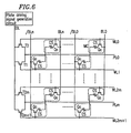
- Figure 6 shows an exemplary conventional nonvolatile semiconductor memory device using this type of ferroelectric. See, for example, T. Sumi et al., 1994 IEEE International Solid-State Circuits Conference, Digest of Technical Papers, pp. 268-269
- the ferroelectric memory device shown in Figure 6 includes a plurality of memory cells MC each including a capacitor Cs and a MOS transistor Qc .
- the capacitor Cs has two opposing electrodes and a ferroelectric film sandwiched by the electrodes.
- One of the electrodes of the capacitor Cs is connected to one of a source electrode and a drain electrode of the MOS transistor Qc .
- the plurality of memory cells MC are arranged in row and column directions.
- a plurality of word lines WL 0 to WL 2m+1 are arranged to correspond to rows of the plurality of memory cells MC , so that each word line is connected to gate electrodes of the transistors Qc of the corresponding row of the memory cells MC .
- the memory cells MC connected to the selected word line are put in a selected state.
- a plurality of bit lines BL 0 to BL n and a plurality of bit bar lines /BL 0 to /BL n are arranged to correspond to columns of the plurality of memory cells MC , so that each of the bit lines and bit bar lines is connected to the other of the source electrode and the drain electrode of each MOS transistor Qc of the corresponding column of the memory cells MC .
- a plurality of plate lines PL 0 to PL m extending in the row direction are arranged every other row of the plurality of memory cells MC , so that each plate line is connected to the other electrode of each of the capacitors Cs of the corresponding two rows of the memory cells MC which is not connected to the corresponding transistor Qc (hereinafter, such an electrode of the capacitor Cs is referred to as a plate electrode).
- a plurality of MOS transistors T 0 to T 2m+1 are arranged to correspond to the plurality of word lines WL 0 to WL 2m+1 so that gate electrodes of the plurality of MOS transistors T 0 to T 2m+1 are connected to the corresponding word lines WL 0 to WL 2m+1 , source electrodes thereof are connected to the corresponding plate lines PL 0 to PL m , and drain electrodes thereof are connected to a drive line DL .
- a plate driving signal generation circuit 1 supplies a plate driving signal to the drive line DL .
- Figure 7 is a timing chart of the ferroelectric memory device shown in Figure 6 .
- a word line e.g., the word line WL 0
- the bit lines BL 0 to BL n the bit bar lines /BL 0 to /BL n
- the drive line DL are in a grounding potential level.
- the word line WL 0 rises to a high level
- the memory cells MC connected to the word line WL 0 turn to a selected state, and the transistor T 0 is turned on, to allow the plate line PL 0 to be connected with the drive line DL .
- the plate driving signal then becomes a high level to provide a plate driving voltage Vp1, which is applied to the plate line PL 0 .
- Vp1 plate driving voltage
- the bit bar lines /BL 0 to /BL n which are paired with the bit lines BL 0 to BL n , respectively, are selectively connected to reference cells (not shown) to generate a reference voltage level.
- the reference voltage is set at a potential just in the middle of potentials at the bit line generated when the information read from the memory cell MC is "1" and when it is "0". This setting is achieved by adjusting the size of a capacitor of each reference cell.
- a voltage difference between the paired ones of the bit lines BL 0 to BL n and the bit bar lines /BL 0 to /BL n is sense-amplified, to read outside the information stored in the memory cells in the selected state. Thereafter, the plate driving signal becomes a low level to provide a grounding potential, which is applied to the plate line PL 0 . This allows information to be written again in the memory cells in the selected state.
- the ferroelectric film of the capacitor Cs of each memory cell MC is provided with positive and negative induced polarization, to store information in the memory cell MC .
- the stored information is read by detecting the state of the induced polarization. For this detection, it is required to supply a predetermined potential, such as the potential Vp1, to the corresponding plate line as described above.
- a predetermined potential such as the potential Vp1
- the capacitor Cs is made of a ferroelectric, the capacitance value thereof tends to be greater than that of a conventional DRAM.
- the plate lines are generally made of precious metal, such as Au, Pt, and Ru, for the conformity with the dielectric of the capacitors. It is difficult to thicken such precious metal since the processability thereof is a problem.
- the conventional ferroelectric memory device has a construction in which the plate lines are driven at a predetermined voltage for each access. This requires a long time for driving the plate lines, making it difficult to realize high-speed operation. Moreover, power consumption increases for charging and discharging of the plate lines.
- US 5 309 391 discloses a two transistor, single capacitor ferroelectric memory cell in which a stepped voltage is applied to the drive line for writing polarization states into the capacitor.
- US 5 357 460 discloses a semiconductor memory device with unit memory cells each with two transistors and a capacitor.
- the column selection plate driving circuit includes a main drive line, a plate driving signal generation circuit for supplying a plate driving signal to the main drive line, and a plurality of MOS transistors, gates of the plurality of MOS transistors are respectively connected to a plurality of address decode signal lines, first electrodes of the plurality of MOS transistors are connected to the main drive line, and second electrodes of the plurality of MOS transistors are respectively connected to the plurality of column selection plate driving lines.
- a preferred embodiment of the semiconductor memory device of this invention includes: a plurality of memory cells arranged in row and column directions, a plurality of word lines extending in the row direction, a plurality of bit lines extending in the column direction, a plurality of bit bar lines extending in the column direction, a plurality of column selection plate driving lines extending in the column direction, and a plurality of second transistors, wherein each of the plurality of memory cells includes a capacitor and a first transistor, the capacitor includes a first electrode, a second electrode opposing the first electrode, and a ferroelectric film sandwiched by the first and second electrodes, and stores and holds binary information utilizing a polarizing state of the ferroelectric film, the first transistor includes a first electrode, a second electrode, and a gate electrode, each of the plurality of second transistors includes a first electrode, a second electrode, and a gate electrode, the first electrode of the first transistor is connected to one of the plurality of bit lines and the plurality of bit bar lines, the second electrode of the first
- the invention described herein makes possible the advantage of providing a semiconductor memory device capable of operating at high speed with reduced power consumption.
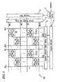
- Figure 1 is a circuit diagram of a ferroelectric memory device 100 of Example 1.
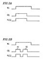
- Figures 2A and 2B are timing charts of the ferroelectric memory device 100 shown in Figure 1 .
- the ferroelectric memory device 100 shown in Figure 1 includes a plurality of memory cells MC arranged in row and column directions. Each of the memory cells MC has a capacitor Cs , a first transistor Qa , and a second transistor Qd .
- the capacitor Cs includes a first electrode and a second electrode opposing the first electrode, with a ferroelectric film sandwiched by the first and second electrodes.
- the capacitor Cs stores and holds binary information utilizing the polarization state of the ferroelectric film.
- the second electrode of the capacitor Cs is also referred to as a plate electrode.
- the first transistor Qa includes source and drain electrodes (one of these electrodes is also referred to as the first electrode, while the other is also referred to as the second electrode), and a gate electrode.
- the second electrode of the first transistor Qa is connected to the first electrode of the capacitor Cs .
- the second transistor Qd includes source and drain electrodes (one of these electrodes is also referred to as the first electrode, while the other is also referred to as the second electrode), and a gate electrode.
- the first electrode of the second transistor Qd is connected to the second electrode of the capacitor Cs .
- a plurality of word lines WL 0 , WL 1 , ... are arranged to correspond to rows of the plurality of memory cells MC , so that each word line is connected to gate electrodes of the transistors Qa and Qd of the corresponding row of the memory cells MC .
- a plurality of bit lines BL 0 , BL 1 , ... and a plurality of bit bar lines /BL 0 , /BL 1 , ... are arranged to correspond to columns of the plurality of memory cells MC , so that each of the bit lines and bit bar lines is connected to the first electrode (one of the source electrode and the drain electrode) of each of the transistors Qa of the corresponding column of the memory cells MC .
- the second electrode (one of the source electrode and the drain electrode) of the transistor Qd of each of the columns of the memory cells MC is connected to corresponding one of a plurality of column selection plate driving lines CD 0 , CD 1 , ....
- the plate electrode of the capacitor Cs as a node is referred to as PL(i,j).
- the ferroelectric memory device 100 shown in Figure 1 further includes: an address buffer 2 which receives an address signal generated externally (or internally); a row decoder 3 and a column decoder 4 which receive a signal output from the address buffer 2 ; a word line driving circuit 5 which receives an address decode signal output from the row decoder 3 and drives the word lines WL 0 , WL 1 , ...; and a column selection plate driving circuit 6 which receives a column address decode signal output from the column decoder 4 and drives the column selection plate driving lines CD 0 , CD 1 , ....
- the column selection plate driving lines CD 0 , CD 1 , ... are made of polysilicon interconnects or normal metal interconnects (such as aluminum interconnects).
- bit lines BL 0 , BL 1 , ..., the bit bar lines /BL 0 , /BL 1 , ..., and the column selection plate driving lines CD 0 , CD 1 , ... are in a grounding potential level.
- a predetermined word line e.g., a word line WL i
- the transistors Qa of the memory cells MC connected to the word line WL i are turned on, to allow the first electrode of each of the capacitors Cs of the memory cells MC to be put in the grounding potential level which is the same as the potential level of the bit lines or the bit bar lines.
- the column selection plate driving lines CD 0 , CD 1 (not shown), ... are connected to the plate electrodes PL(i,0), PL(i,1) (not shown), ..., respectively.
- the bit bar line /BL j which is paired with the bit line BL j is put in a reference voltage level by selecting a reference cell (not shown). Information stored in the memory cell in the selected state can be read outside by sense-amplifying a potential difference between the pair of the bit line BL j and the bit bar line /BL j .
- any non-selected memory cell which is not in the j-th column no potential difference is generated between the pair of the bit line and the bit bar line. Accordingly, information stored in such a memory cell is not sense-amplified to be read outside. In other words, only the memory cell MC located in the i-th row and the j-th column is sense-amplified.
- the signal at the column selection plate driving line CD j becomes the grounding potential level, and thus the voltage at the plate electrode PL(i,j) becomes the grounding potential.
- a read and a rewrite are completed by one pulse of the column selection plate driving signal.
- the ferroelectric memory device 100 may be operated according to the timing chart shown in Figure 2B .
- a read is completed by a pulse P1 of the column selection plate driving signal and then a rewrite is ensured by a subsequent pulse P2 of the column selection plate driving signal.
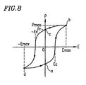
- the rewrite as used herein refers to an operation as follows. Referring to Figure 8 , in the read operation described above, the state at point c has been changed to the state at point a , resulting in breaking the data at point c . Thus, a positive electric field Emax is applied to the ferroelectric film of the capacitor, to resume the state at point c .
- any non-selected memory cell MC which is not in the i-th row since the capacitor Cs of the memory cells MC is isolated from the bit line (or the bit bar line) by the transistors Qa and Qd , the voltage between the electrodes of the capacitor Cs does not vary, irrespective of whether or not the voltage Vp1 is applied to the column plate driving line CD x (x is an integer excluding i), preventing the polarization information from being broken.
- any memory cell MC which is connected to the selected word line WL i and connected to the column selection plate driving lines CD in a non-selected level no sense-amplification is performed, preventing the polarization information from being broken.
- the column selection plate driving circuit 6 is only required to drive the plate electrode PL(i,j) of a single memory cell MC for each access operation, and thus the capacitance value and resistance value thereof are small. This reduces the time required to drive the plate electrode and thus realizes high-speed operation and low power consumption. Moreover, since only information stored in a single memory cell MC is sense-amplified, the current consumption in the sense-amplification is also greatly reduced.
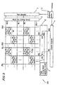
- FIG. 3 is a circuit diagram of a ferroelectric emory device 200 of Example 2.
- the ferroelectric memory evice 200 includes a plurality of memory cells MC, a lurality of word lines WL 0 , WL 1 , ..., a plurality of bit lines BL 0 , BL 1 , ..., a plurality of bit bar lines /BL 0 , /BL 1 , ..., and a column selection plate driving circuit 6' .
- the construction of the ferroelectric memory device 200 shown in Figure 3 is the same as that of the ferroelectric memory device 100 except for the column selection plate driving circuit 6' .
- the same components as those of the ferroelectric memory device 100 are denoted by the same reference numerals, and the description thereof is basically omitted.
- the column selection plate driving circuit 6' includes a main drive line 8 , a plate driving signal generation circuit 7 which outputs a plate driving signal to the main drive line 8 , and a plurality of MOS transistors QC 0 , ... QC j , ....
- Gates of the plurality of MOS transistors QC 0 , ... QC j , .... are connected to address decode signal lines AD 0 , ... , AD j , ... connected to the column decoder 4, respectively.
- Drains or sources of the plurality of MOS transistors QC 0 , ... QC j , ... are commonly connected to the main drive line 8 .
- the others of the drains and sources of the plurality of MOS transistors QC 0 , ... QC j , ... are connected to the column selection plate driving lines CD 0 , ..., CD j , ..., respectively.
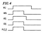
- Figure 4 is a timing chart of the ferroelectric memory device 200 .
- the bit lines BL 0 , BL 1 , ..., the bit bar lines /BL 0 , /BL 1 , ..., and the column selection plate driving lines CD 0 , CD 1 , ... are in a grounding potential level.
- a word line (e.g., the word line WL i ) becomes a selected level in response to the row address signal.
- the transistors Qa of the memory cells MC connected to the selected word line WL are turned on, to allow the first electrode of each of the capacitors Cs of the memory cells MC to be put in the grounding potential level which is the same as the potential level of the bit lines or the bit bar lines.
- the transistors Qd of the memory cells MC connected to the selected word line WL are also turned on, to allow the second electrode of each of the capacitors Cs to be connected to the corresponding column selection plate driving line CD .
- the plate driving signal generation circuit 7 outputs a main drive signal MDL (a high voltage Vp1) as a plate driving signal, to the main drive line 8 .
- the column decoder 4 outputs address decode signals ADS 0 , ..., ADS j , ... to the column selection plate driving circuit 6' .
- the column selection plate driving circuit 6' selects at least one column selection plate driving line CD based on the address decode signals ADS 0 , ..., ADS j , ....
- the main drive signal MDL is then supplied to the selected column selection plate driving line CD .
- Example 1 As a result, as in Example 1 described above, only information stored in the memory cell MC in the i-th row and the j-th column is read to the bit line BL j and sense-amplified. The sense-amplified information is then read outside. After the read operation, while the address decode signal AD j is still in the selected level, the main drive line 8 is returned to the grounding potential level. This turns again the column selection plate driving signal line CD j and the plate electrode PL(i,j) to the grounding potential level, to allow information to be written again in the memory cell in the selected state.
- FIG. 5 is a circuit diagram of a ferroelectric emory device 300 of Example 3.
- the ferroelectric memory device 300 includes a plurality of memory cells MC , a plurality of word lines WL 0 , WL 1 , ..., a plurality of bit lines BL 0 , BL 1 , ..., a plurality of bit bar lines /BL 0 , /BL 1 , ..., and a column selection plate driving circuit 6" .
- Example 3 the a-th to (a+j)-th columns are regarded as one unit.
- the bit lines BL 0 to BL j and the bit bar lines /BL 0 to /BL j are regarded as one unit, while the bit lines BL j+1 to BL 2j+1 and the bit bar lines /BL j+1 to /BL 2j+1 are regarded as one unit.
- the first electrodes of the capacitors Cs of the memory cells MC which are in the 0-th to (0+j)-th rows are connected to the transistors Qa of the respective memory cells MC .
- the second electrodes of the capacitors Cs of the memory cells MC which are in the 0-th to (0+j)-th row are connected to one common transistor Qd via a certain plate line.
- the each gate electrode of the transistors Qa and Qd is connected to the word line WL .
- the second electrodes of the capacitors Cs of the plurality of memory cells MC connected to the word line WL 0 and connected to the bit lines BL 0 to BL j are connected to the first electrode of the transistor Qd 0 via a certain plate line.
- the gate electrode of the transistor Qd 0 is connected to the word line WL 0 .
- the second electrodes of the capacitors Cs of the plurality of memory cells MC connected to the word line WL 1 and connected to the bit bar lines /BL 0 to /BL j are connected to the first electrode of the transistor Qd 1 via a certain plate line.
- the gate electrode of the transistor Qd 1 is connected to the word line WL 1 .
- the second electrodes of the capacitors Cs of the plurality of memory cells MC connected to the word line WL i and connected to the bit lines BL 0 to BL j are connected to the first electrode of the transistor Qd i via a certain plate line.
- the gate electrode of the transistor Qd i is connected to the word line WL i .
- the second electrodes of the transistors Qd 0 , ..., Qd i are connected to the common column selection plate driving line CD 0 .
- the first electrode as used herein is referred to as either one of the source and the drain of a transistor, while the second electrode as used herein is referred to as the other of the source and the drain.
- the second electrodes of the capacitors Cs of the plurality of memory cells MC connected to the word lines WL i and connected to the bit lines BL j+1 to BL 2j+1 or the bit bar lines /BL j+1 to /BL 2j+1 are connected to the common column selection plate driving line CD 1 via the corresponding transistors.
- the column selection plate driving circuit 6" includes a main drive line 8 , a plate driving signal generation circuit 7 which outputs a plate driving signal to the main drive line 8 , and a plurality of MOS transistors QC 0 , ... QC j , ....
- Gates of the plurality of MOS transistors QC 0 , ... QC j , .... are connected to address decode signal lines AD 0 , ..., AD j , ... connected to the column decoder 4 , respectively.
- the first electrodes of the plurality of MOS transistors QC 0 , ... QC j are commonly connected to the main drive line 8 .
- the second electrodes of the plurality of MOS transistors QC 0 , ... QC j are commonly connected to the column selection plate driving line CD 0 .
- the first electrode as used herein is referred to as either one of the source and the drain of a transistor, while the second electrode as used herein is referred to as the other of the source and the drain.
- the common column selection plate driving line CD 0 is configured to transmit an output of the plate driving signal generation circuit 7 when any of the 0-th to j-th columns is selected in response to the address decode signal output from the column decoder 4 .
- address decode signals for the 0-th to j-th columns are input into gates of the transistors Qc 0 to Qc j , respectively.
- the number of the transistors Qd required in the ferroelectric memory device can be reduced to 1/(j+1). This reduces the area of the memory cells MC and thus reduces the production cost of the ferroelectric memory device.
- the plate of the memory cells is divided into sections in row and column directions. This makes it possible to select and operate only one memory cell among the plurality of memory cells by a single access operation of the semiconductor memory device. As a result, the plate driving time can be reduced, compared with the conventional semiconductor memory device, and thus high-speed operation of the memory cells is possible. Additionally, in the semiconductor memory device according to the present invention, power consumption can be reduced.
Landscapes
- Engineering & Computer Science (AREA)
- Computer Hardware Design (AREA)
- Dram (AREA)
- Semiconductor Memories (AREA)
- Thin Film Transistor (AREA)
- Semiconductor Integrated Circuits (AREA)
Claims (3)
- Halbleiterspeichervorrichtung (100) mit wenigstens einer Speicherzelle (MC), wobei die oder jede Speicherzelle (MC) einen Kondensator (Cs), einen ersten Transistor (Qa) und einen zweiten Transistor (Qd) aufweist, wobei
der Kondensator (Cs) eine erste Elektrode, eine zweite Elektrode, die der ersten Elektrode gegenüberliegt, und einen ferroelektrischen Film aufweist, der zwischen der ersten und zweiten Elektrode angeordnet ist, wobei der Kondensator unter Verwendung eines Polarisationszustandes des ferroelektrischen Films Binärinformationen speichert und beinhaltet,
der erste Transistor (Qa) eine erste Elektrode, eine zweite Elektrode und eine Gate-Elektrode aufweist, wobei die zweite Elektrode mit der ersten Elektrode des Kondensators (Cs) verbunden ist, und
der zweite Transistor (Qd) eine erste Elektrode, eine zweite Elektrode und eine Gate-Elektrode aufweist, wobei die erste Elektrode mit der zweiten Elektrode des Kondensators (Cs) verbunden ist,
dadurch gekennzeichnet, dass
die Speicherzelle (MC) des weiteren eine Wortleitung (WLj), eine Bitleitung. (BLj), eine Bit-Schienen-Leitung (/BLj) und eine Mehrzahl von Spaltenauswahl-Platten-Versorgungsleitungen (CD0, CD1...) aufweist, wobei
die erste Elektrode des ersten Transistors (Qa) mit der Bitleitung (BLj) oder Bit-Schienen-Leitung (/BLj) verbunden ist,
die Gate-Elektrode des ersten Transistors (Qa) mit der Wortleitung (WLj) verbunden ist,
die zweite Elektrode des zweiten Transistors (Qd) mit einer der Mehrzahl von Spaltenauswahl-Platten-Versorgungsleitungen (CD0, CD1,...) verbunden ist, und
die Gate-Elektrode des zweiten Transistors (Qd) mit der Wortleitung (WLj) verbunden ist,
wobei die Zelle (MC) des weiteren eine Spaltenauswahl-Platten-Versorgungsschaltung zum Auswählen einer aus der Mehrzahl von Spaltenauswahl-Platten-Versorgungsleitungen auf der Basis eines Spaltenadress-Entschlüsselungssignals aufweist. - Halbleiterspeichervorrichtung nach Anspruch 1, wobei die Spaltenauswahl-Platten-Versorgungsschaltung eine Hauptversorgungsleitung, eine Platten-Versorgungssignal-Erzeugungsschaltung zum Liefern eines Platten-Versorgungssignals zur Hauptversorgungsleitung und eine Mehrzahl von MOS-Transistoren aufweist,
die Gates der Mehrzahl von MOS-Transistoren jeweils mit einer Mehrzahl von Adress-Entschlüsselungs-Signalleitungen verbunden sind,
die ersten Elektroden der Mehrzahl von MOS-Transistoren mit der Hauptversorgungsleitung verbunden sind, und
die zweiten Elektroden der Mehrzahl von MOS-Transistoren jeweils mit der Mehrzahl von Spaltenauswahl-Platten-Versorgungsleitungen verbunden sind. - Halbleiterspeichervorrichtung nach Anspruch 1, mit einer Mehrzahl von Speicherzellen (MC), die in Zeilen und Spalten angeordnet sind, einer Mehrzahl von Wortleitungen, die sich in der Richtung der Zeilen erstrecken, einer Mehrzahl von Bitleitungen, die sich in der Richtung der Spalten erstrecken, einer Mehrzahl von Bit-Schienen-Leitungen, die sich in der Richtung der Spalten erstrecken, einer Mehrzahl von Spaltenauswahl-Platten-Versorgungsleitungen, die sich in der Richtung der Spalten erstrecken, und einer Mehrzahl von zweiten Transistoren, wobei
jede aus der Mehrzahl von Speicherzellen (MC) einen Kondensator (Cs) und einen ersten Transistor (Qa) aufweist,
die Mehrzahl von Speicherzellen (MC) in eine Mehrzahl von Gruppen klassifiziert ist,
die zweiten Elektroden der Kondensatoren (Cs) einer Mehrzahl von Speicherzellen einer Gruppe in einer ersten Zeile mit der ersten Elektrode von einem aus der Mehrzahl von zweiten Transistoren mittels einer Platten-Leitung verbunden sind,
die zweite Elektrode des einen der Mehrzahl von zweiten Transistoren (Qd) in der ersten Zeile mit einer der Mehrzahl von Spaltenauswahl-Platten-Versorgungsleitungen verbunden ist,
die Gate-Elektrode des einen aus der Mehrzahl von zweiten Transistoren in der ersten Zeile mit einer aus der Mehrzahl von Wortleitungen (WLj) verbunden ist,
die Gate-Elektrode des ersten Transistors (Qa) in der ersten Zeile mit derjenigen Wortleitung verbunden ist, mit der der zweite Transistor (Qd) in der ersten Zeile verbunden ist.
die zweiten Elektroden der Kondensatoren einer Mehrzahl von Speicherzellen (MC) einer Gruppe in einer zweiten Zeile mit der ersten Elektrode eines aus der Mehrzahl von zweiten Transistoren über eine Platten-Leitung verbunden sind, die zweite Elektrode des einen aus der Mehrzahl von zweiten Transistoren in der zweiten Reihe mit einer aus der Mehrzahl von Spaltenauswahl-Platten-Versorgungsleitungen (CD0, CD1...) verbunden ist,
die Gate-Elektrode des einen aus der Mehrzahl von zweiten Transistoren in der zweiten Zeile mit einer aus der Mehrzahl von Wortleitungen verbunden ist, und
die Gate-Elektrode des ersten Transistors (Qa) in der zweiten Zeile mit derjenigen Wortleitung verbunden ist, mit der der zweite Transistor in der zweiten Zeile verbunden ist.
Applications Claiming Priority (2)
| Application Number | Priority Date | Filing Date | Title |
|---|---|---|---|
| JP3715298 | 1998-02-19 | ||
| JP03715298A JP3495905B2 (ja) | 1998-02-19 | 1998-02-19 | 半導体記憶装置 |
Publications (3)
| Publication Number | Publication Date |
|---|---|
| EP0938096A2 EP0938096A2 (de) | 1999-08-25 |
| EP0938096A3 EP0938096A3 (de) | 2000-08-16 |
| EP0938096B1 true EP0938096B1 (de) | 2004-10-20 |
Family
ID=12489645
Family Applications (1)
| Application Number | Title | Priority Date | Filing Date |
|---|---|---|---|
| EP99301080A Expired - Lifetime EP0938096B1 (de) | 1998-02-19 | 1999-02-15 | Ferroelektrische Speicheranordnung |
Country Status (6)
| Country | Link |
|---|---|
| US (1) | US6154387A (de) |
| EP (1) | EP0938096B1 (de) |
| JP (1) | JP3495905B2 (de) |
| KR (1) | KR100314491B1 (de) |
| DE (1) | DE69921215T2 (de) |
| TW (1) | TW416050B (de) |
Families Citing this family (25)
| Publication number | Priority date | Publication date | Assignee | Title |
|---|---|---|---|---|
| JP3377762B2 (ja) * | 1999-05-19 | 2003-02-17 | 株式会社半導体理工学研究センター | 強誘電体不揮発性メモリ |
| DE10008243B4 (de) | 2000-02-23 | 2005-09-22 | Infineon Technologies Ag | Integrierter Speicher mit Plattenleitungssegmenten |
| JP4047531B2 (ja) * | 2000-10-17 | 2008-02-13 | 株式会社東芝 | 強誘電体メモリ装置 |
| CN100336226C (zh) * | 2001-12-14 | 2007-09-05 | 株式会社日立制作所 | 半导体器件 |
| US6809949B2 (en) | 2002-05-06 | 2004-10-26 | Symetrix Corporation | Ferroelectric memory |
| JP2004220705A (ja) * | 2003-01-15 | 2004-08-05 | Seiko Epson Corp | 強誘電体記憶装置 |
| JP2007053321A (ja) * | 2005-08-19 | 2007-03-01 | Matsushita Electric Ind Co Ltd | 半導体記憶装置 |
| US7164595B1 (en) * | 2005-08-25 | 2007-01-16 | Micron Technology, Inc. | Device and method for using dynamic cell plate sensing in a DRAM memory cell |
| WO2007086438A1 (ja) * | 2006-01-27 | 2007-08-02 | Kyocera Corporation | 無線通信端末及び配信コンテンツ受信方法 |
| JP4887853B2 (ja) * | 2006-03-17 | 2012-02-29 | 富士通セミコンダクター株式会社 | 半導体記憶装置 |
| JP4872976B2 (ja) * | 2008-07-07 | 2012-02-08 | セイコーエプソン株式会社 | 強誘電体メモリ装置 |
| EP3507832A4 (de) | 2016-08-31 | 2020-04-08 | Micron Technology, Inc. | Speicherzellen und speicherarrays |
| SG11201901210UA (en) | 2016-08-31 | 2019-03-28 | Micron Technology Inc | Ferroelectric memory cells |
| EP3840046A1 (de) | 2016-08-31 | 2021-06-23 | Micron Technology, Inc. | Speicherzellen und speicherarrays |
| EP3507802A4 (de) | 2016-08-31 | 2020-04-08 | Micron Technology, Inc. | Sensorverstärkerkonstruktionen |
| JP6777369B2 (ja) | 2016-08-31 | 2020-10-28 | マイクロン テクノロジー,インク. | 強誘電体メモリを含み、強誘電体メモリを動作するための装置及び方法 |
| CN109155311A (zh) | 2016-08-31 | 2019-01-04 | 美光科技公司 | 存储器单元及存储器阵列 |
| US10355002B2 (en) | 2016-08-31 | 2019-07-16 | Micron Technology, Inc. | Memory cells, methods of forming an array of two transistor-one capacitor memory cells, and methods used in fabricating integrated circuitry |
| WO2018044510A1 (en) | 2016-08-31 | 2018-03-08 | Micron Technology, Inc. | Apparatuses and methods including two transistor-one capacitor memory and for accessing same |
| KR102188490B1 (ko) | 2016-08-31 | 2020-12-09 | 마이크론 테크놀로지, 인크. | 강유전체 메모리를 포함하며 강유전체 메모리에 액세스하기 위한 장치 및 방법 |
| WO2018044453A1 (en) | 2016-08-31 | 2018-03-08 | Micron Technology, Inc. | Memory cells and memory arrays |
| EP3507808A4 (de) | 2016-08-31 | 2020-05-27 | Micron Technology, Inc. | Speicherarrays |
| CN110192280A (zh) | 2017-01-12 | 2019-08-30 | 美光科技公司 | 存储器单元、双晶体管单电容器存储器单元阵列、形成双晶体管单电容器存储器单元阵列的方法及用于制造集成电路的方法 |
| US10867675B2 (en) | 2017-07-13 | 2020-12-15 | Micron Technology, Inc. | Apparatuses and methods for memory including ferroelectric memory cells and dielectric memory cells |
| CN110753962A (zh) | 2017-08-29 | 2020-02-04 | 美光科技公司 | 存储器电路 |
Family Cites Families (6)
| Publication number | Priority date | Publication date | Assignee | Title |
|---|---|---|---|---|
| US4888733A (en) * | 1988-09-12 | 1989-12-19 | Ramtron Corporation | Non-volatile memory cell and sensing method |
| US5357460A (en) * | 1991-05-28 | 1994-10-18 | Sharp Kabushiki Kaisha | Semiconductor memory device having two transistors and at least one ferroelectric film capacitor |
| US5309391A (en) * | 1992-10-02 | 1994-05-03 | National Semiconductor Corporation | Symmetrical polarization enhancement in a ferroelectric memory cell |
| JP3767703B2 (ja) * | 1995-11-16 | 2006-04-19 | ローム株式会社 | 強誘電体記憶装置および強誘電体コンデンサを用いた記憶方法 |
| US5764561A (en) * | 1995-11-16 | 1998-06-09 | Rohm Co., Ltd. | Ferroelectric memory devices and method of using ferroelectric capacitors |
| US5917746A (en) * | 1997-08-27 | 1999-06-29 | Micron Technology, Inc. | Cell plate structure for a ferroelectric memory |
-
1998
- 1998-02-19 JP JP03715298A patent/JP3495905B2/ja not_active Expired - Fee Related
-
1999
- 1999-02-12 US US09/249,477 patent/US6154387A/en not_active Expired - Fee Related
- 1999-02-12 TW TW088102223A patent/TW416050B/zh not_active IP Right Cessation
- 1999-02-15 DE DE69921215T patent/DE69921215T2/de not_active Expired - Fee Related
- 1999-02-15 EP EP99301080A patent/EP0938096B1/de not_active Expired - Lifetime
- 1999-02-18 KR KR1019990005350A patent/KR100314491B1/ko not_active IP Right Cessation
Also Published As
| Publication number | Publication date |
|---|---|
| EP0938096A3 (de) | 2000-08-16 |
| KR100314491B1 (ko) | 2001-11-15 |
| KR19990072706A (ko) | 1999-09-27 |
| EP0938096A2 (de) | 1999-08-25 |
| TW416050B (en) | 2000-12-21 |
| JPH11238386A (ja) | 1999-08-31 |
| DE69921215D1 (de) | 2004-11-25 |
| DE69921215T2 (de) | 2005-11-10 |
| US6154387A (en) | 2000-11-28 |
| JP3495905B2 (ja) | 2004-02-09 |
Similar Documents
| Publication | Publication Date | Title |
|---|---|---|
| EP0938096B1 (de) | Ferroelektrische Speicheranordnung | |
| US5917746A (en) | Cell plate structure for a ferroelectric memory | |
| US5574698A (en) | Ram row decode circuitry that utilizes a precharge circuit that is deactivated by a feedback from an activated word line driver | |
| US5751626A (en) | Ferroelectric memory using ferroelectric reference cells | |
| JP3183076B2 (ja) | 強誘電体メモリ装置 | |
| US5608667A (en) | Ferroelectric memory automatically generating biasing pulse for plate electrode | |
| US5373463A (en) | Ferroelectric nonvolatile random access memory having drive line segments | |
| US5847989A (en) | Ferroelectric memory using non-remnant reference circuit | |
| US5999439A (en) | Ferroelectric memory using ferroelectric reference cells | |
| US6859380B2 (en) | Ferroelectric memory and method of operating same | |
| US6240007B1 (en) | Nonvolatile ferroelectric memory device having global and local bitlines and split workline driver | |
| JPH10106272A (ja) | 半導体記憶装置 | |
| JPH06208796A (ja) | 半導体メモリ | |
| KR100323985B1 (ko) | 반도체 기억 장치 | |
| US6297985B1 (en) | Cell block structure of nonvolatile ferroelectric memory | |
| JP4490514B2 (ja) | 強誘電体メモリ | |
| US6807083B2 (en) | Ferroelectric memory device | |
| EP0944092B1 (de) | Nichtflüchtige Halbleiterspeicheranordnung | |
| US6438020B1 (en) | Ferroelectric memory device having an internal supply voltage, which is lower than the external supply voltage, supplied to the memory cells | |
| US7251153B2 (en) | Memory | |
| US6320783B1 (en) | Nonvolatile ferroelectric memory device and circuit for driving the same | |
| US6690198B2 (en) | Repeater with reduced power consumption | |
| JPH0845285A (ja) | 半導体記憶装置 | |
| US6538913B2 (en) | Method for operating a ferroelectric memory configuration and a ferroelectric memory configuration | |
| US6990007B2 (en) | Semiconductor memory device |
Legal Events
| Date | Code | Title | Description |
|---|---|---|---|
| PUAI | Public reference made under article 153(3) epc to a published international application that has entered the european phase |
Free format text: ORIGINAL CODE: 0009012 |
|
| AK | Designated contracting states |
Kind code of ref document: A2 Designated state(s): DE FR GB |
|
| AX | Request for extension of the european patent |
Free format text: AL;LT;LV;MK;RO;SI |
|
| PUAL | Search report despatched |
Free format text: ORIGINAL CODE: 0009013 |
|
| AK | Designated contracting states |
Kind code of ref document: A3 Designated state(s): AT BE CH CY DE DK ES FI FR GB GR IE IT LI LU MC NL PT SE |
|
| AX | Request for extension of the european patent |
Free format text: AL;LT;LV;MK;RO;SI |
|
| 17P | Request for examination filed |
Effective date: 20010109 |
|
| AKX | Designation fees paid |
Free format text: DE FR GB |
|
| 17Q | First examination report despatched |
Effective date: 20030827 |
|
| GRAP | Despatch of communication of intention to grant a patent |
Free format text: ORIGINAL CODE: EPIDOSNIGR1 |
|
| GRAS | Grant fee paid |
Free format text: ORIGINAL CODE: EPIDOSNIGR3 |
|
| GRAA | (expected) grant |
Free format text: ORIGINAL CODE: 0009210 |
|
| AK | Designated contracting states |
Kind code of ref document: B1 Designated state(s): DE FR GB |
|
| REG | Reference to a national code |
Ref country code: GB Ref legal event code: FG4D |
|
| REF | Corresponds to: |
Ref document number: 69921215 Country of ref document: DE Date of ref document: 20041125 Kind code of ref document: P |
|
| PLBE | No opposition filed within time limit |
Free format text: ORIGINAL CODE: 0009261 |
|
| STAA | Information on the status of an ep patent application or granted ep patent |
Free format text: STATUS: NO OPPOSITION FILED WITHIN TIME LIMIT |
|
| ET | Fr: translation filed | ||
| 26N | No opposition filed |
Effective date: 20050721 |
|
| PGFP | Annual fee paid to national office [announced via postgrant information from national office to epo] |
Ref country code: DE Payment date: 20090213 Year of fee payment: 11 |
|
| PGFP | Annual fee paid to national office [announced via postgrant information from national office to epo] |
Ref country code: GB Payment date: 20090211 Year of fee payment: 11 |
|
| PGFP | Annual fee paid to national office [announced via postgrant information from national office to epo] |
Ref country code: FR Payment date: 20090213 Year of fee payment: 11 |
|
| GBPC | Gb: european patent ceased through non-payment of renewal fee |
Effective date: 20100215 |
|
| REG | Reference to a national code |
Ref country code: FR Ref legal event code: ST Effective date: 20101029 |
|
| PG25 | Lapsed in a contracting state [announced via postgrant information from national office to epo] |
Ref country code: FR Free format text: LAPSE BECAUSE OF NON-PAYMENT OF DUE FEES Effective date: 20100301 |
|
| PG25 | Lapsed in a contracting state [announced via postgrant information from national office to epo] |
Ref country code: DE Free format text: LAPSE BECAUSE OF NON-PAYMENT OF DUE FEES Effective date: 20100901 |
|
| PG25 | Lapsed in a contracting state [announced via postgrant information from national office to epo] |
Ref country code: GB Free format text: LAPSE BECAUSE OF NON-PAYMENT OF DUE FEES Effective date: 20100215 |