EP0936681A2 - Fotoleitende Dünnschicht und diese Dünnschicht anwendende photovoltaische Vorrichtung - Google Patents
Fotoleitende Dünnschicht und diese Dünnschicht anwendende photovoltaische Vorrichtung Download PDFInfo
- Publication number
- EP0936681A2 EP0936681A2 EP99103051A EP99103051A EP0936681A2 EP 0936681 A2 EP0936681 A2 EP 0936681A2 EP 99103051 A EP99103051 A EP 99103051A EP 99103051 A EP99103051 A EP 99103051A EP 0936681 A2 EP0936681 A2 EP 0936681A2
- Authority
- EP
- European Patent Office
- Prior art keywords
- photovoltaic device
- layer
- thin film
- silicon
- crystal grains
- Prior art date
- Legal status (The legal status is an assumption and is not a legal conclusion. Google has not performed a legal analysis and makes no representation as to the accuracy of the status listed.)
- Withdrawn
Links
- 239000010409 thin film Substances 0.000 title claims abstract description 236
- 239000013078 crystal Substances 0.000 claims abstract description 120
- UFHFLCQGNIYNRP-UHFFFAOYSA-N Hydrogen Chemical compound [H][H] UFHFLCQGNIYNRP-UHFFFAOYSA-N 0.000 claims abstract description 114
- 239000001257 hydrogen Substances 0.000 claims abstract description 108
- 229910052739 hydrogen Inorganic materials 0.000 claims abstract description 108
- 239000000758 substrate Substances 0.000 claims abstract description 101
- 229910052710 silicon Inorganic materials 0.000 claims abstract description 91
- 239000010703 silicon Substances 0.000 claims abstract description 91
- 239000010408 film Substances 0.000 claims abstract description 41
- 238000000034 method Methods 0.000 claims abstract description 27
- XUIMIQQOPSSXEZ-UHFFFAOYSA-N Silicon Chemical compound [Si] XUIMIQQOPSSXEZ-UHFFFAOYSA-N 0.000 claims description 91
- 229910021417 amorphous silicon Inorganic materials 0.000 claims description 63
- 239000007789 gas Substances 0.000 claims description 38
- 229910008314 Si—H2 Inorganic materials 0.000 claims description 21
- XOLBLPGZBRYERU-UHFFFAOYSA-N tin dioxide Chemical compound O=[Sn]=O XOLBLPGZBRYERU-UHFFFAOYSA-N 0.000 claims description 20
- 230000003746 surface roughness Effects 0.000 claims description 17
- 238000005268 plasma chemical vapour deposition Methods 0.000 claims description 13
- 238000004544 sputter deposition Methods 0.000 claims description 13
- 238000002441 X-ray diffraction Methods 0.000 claims description 12
- BQCADISMDOOEFD-UHFFFAOYSA-N Silver Chemical compound [Ag] BQCADISMDOOEFD-UHFFFAOYSA-N 0.000 claims description 11
- 229910021421 monocrystalline silicon Inorganic materials 0.000 claims description 11
- HBMJWWWQQXIZIP-UHFFFAOYSA-N silicon carbide Chemical compound [Si+]#[C-] HBMJWWWQQXIZIP-UHFFFAOYSA-N 0.000 claims description 11
- 229910052709 silver Inorganic materials 0.000 claims description 11
- 239000004332 silver Substances 0.000 claims description 11
- OWXLRKWPEIAGAT-UHFFFAOYSA-N [Mg].[Cu] Chemical compound [Mg].[Cu] OWXLRKWPEIAGAT-UHFFFAOYSA-N 0.000 claims description 10
- 229910052782 aluminium Inorganic materials 0.000 claims description 8
- XAGFODPZIPBFFR-UHFFFAOYSA-N aluminium Chemical compound [Al] XAGFODPZIPBFFR-UHFFFAOYSA-N 0.000 claims description 8
- 239000010949 copper Substances 0.000 claims description 8
- RYGMFSIKBFXOCR-UHFFFAOYSA-N Copper Chemical compound [Cu] RYGMFSIKBFXOCR-UHFFFAOYSA-N 0.000 claims description 7
- 229910052802 copper Inorganic materials 0.000 claims description 7
- 230000015556 catabolic process Effects 0.000 abstract description 25
- 238000006731 degradation reaction Methods 0.000 abstract description 25
- 230000007774 longterm Effects 0.000 abstract description 3
- 239000010410 layer Substances 0.000 description 363
- 238000006243 chemical reaction Methods 0.000 description 37
- 229910021424 microcrystalline silicon Inorganic materials 0.000 description 31
- 125000004429 atom Chemical group 0.000 description 29
- 230000000052 comparative effect Effects 0.000 description 24
- 238000005259 measurement Methods 0.000 description 22
- 238000010521 absorption reaction Methods 0.000 description 21
- 230000015572 biosynthetic process Effects 0.000 description 14
- XYFCBTPGUUZFHI-UHFFFAOYSA-N Phosphine Chemical compound P XYFCBTPGUUZFHI-UHFFFAOYSA-N 0.000 description 13
- BLRPTPMANUNPDV-UHFFFAOYSA-N Silane Chemical compound [SiH4] BLRPTPMANUNPDV-UHFFFAOYSA-N 0.000 description 12
- 239000000463 material Substances 0.000 description 12
- 239000000969 carrier Substances 0.000 description 10
- 239000011521 glass Substances 0.000 description 10
- 229910000073 phosphorus hydride Inorganic materials 0.000 description 10
- WTEOIRVLGSZEPR-UHFFFAOYSA-N boron trifluoride Chemical compound FB(F)F WTEOIRVLGSZEPR-UHFFFAOYSA-N 0.000 description 9
- 238000003917 TEM image Methods 0.000 description 8
- 229910021420 polycrystalline silicon Inorganic materials 0.000 description 8
- 229910015900 BF3 Inorganic materials 0.000 description 7
- 230000007547 defect Effects 0.000 description 7
- XLOMVQKBTHCTTD-UHFFFAOYSA-N Zinc monoxide Chemical compound [Zn]=O XLOMVQKBTHCTTD-UHFFFAOYSA-N 0.000 description 6
- 230000004913 activation Effects 0.000 description 6
- 230000005684 electric field Effects 0.000 description 6
- VNWKTOKETHGBQD-UHFFFAOYSA-N methane Chemical compound C VNWKTOKETHGBQD-UHFFFAOYSA-N 0.000 description 6
- 230000035945 sensitivity Effects 0.000 description 6
- 229910000577 Silicon-germanium Inorganic materials 0.000 description 5
- 230000008859 change Effects 0.000 description 5
- 229910021419 crystalline silicon Inorganic materials 0.000 description 5
- 150000002431 hydrogen Chemical class 0.000 description 5
- OKTJSMMVPCPJKN-UHFFFAOYSA-N Carbon Chemical compound [C] OKTJSMMVPCPJKN-UHFFFAOYSA-N 0.000 description 4
- 238000001237 Raman spectrum Methods 0.000 description 4
- 229910052799 carbon Inorganic materials 0.000 description 4
- 238000010894 electron beam technology Methods 0.000 description 4
- 230000008569 process Effects 0.000 description 4
- 238000011160 research Methods 0.000 description 4
- 238000001771 vacuum deposition Methods 0.000 description 4
- 229910052796 boron Inorganic materials 0.000 description 3
- 230000007423 decrease Effects 0.000 description 3
- 230000000694 effects Effects 0.000 description 3
- 230000031700 light absorption Effects 0.000 description 3
- 238000004519 manufacturing process Methods 0.000 description 3
- 230000003287 optical effect Effects 0.000 description 3
- 230000006798 recombination Effects 0.000 description 3
- 238000005215 recombination Methods 0.000 description 3
- 239000002356 single layer Substances 0.000 description 3
- 239000007787 solid Substances 0.000 description 3
- 238000001228 spectrum Methods 0.000 description 3
- IJGRMHOSHXDMSA-UHFFFAOYSA-N Atomic nitrogen Chemical compound N#N IJGRMHOSHXDMSA-UHFFFAOYSA-N 0.000 description 2
- ZOXJGFHDIHLPTG-UHFFFAOYSA-N Boron Chemical compound [B] ZOXJGFHDIHLPTG-UHFFFAOYSA-N 0.000 description 2
- OAICVXFJPJFONN-UHFFFAOYSA-N Phosphorus Chemical compound [P] OAICVXFJPJFONN-UHFFFAOYSA-N 0.000 description 2
- 238000000137 annealing Methods 0.000 description 2
- 230000003247 decreasing effect Effects 0.000 description 2
- 238000009792 diffusion process Methods 0.000 description 2
- AMGQUBHHOARCQH-UHFFFAOYSA-N indium;oxotin Chemical compound [In].[Sn]=O AMGQUBHHOARCQH-UHFFFAOYSA-N 0.000 description 2
- 238000002329 infrared spectrum Methods 0.000 description 2
- 239000003921 oil Substances 0.000 description 2
- 229910052698 phosphorus Inorganic materials 0.000 description 2
- 239000011574 phosphorus Substances 0.000 description 2
- 230000002265 prevention Effects 0.000 description 2
- 229910000077 silane Inorganic materials 0.000 description 2
- 229910001220 stainless steel Inorganic materials 0.000 description 2
- 239000010935 stainless steel Substances 0.000 description 2
- 238000004627 transmission electron microscopy Methods 0.000 description 2
- 239000011787 zinc oxide Substances 0.000 description 2
- ZAMOUSCENKQFHK-UHFFFAOYSA-N Chlorine atom Chemical compound [Cl] ZAMOUSCENKQFHK-UHFFFAOYSA-N 0.000 description 1
- PXGOKWXKJXAPGV-UHFFFAOYSA-N Fluorine Chemical compound FF PXGOKWXKJXAPGV-UHFFFAOYSA-N 0.000 description 1
- 238000004566 IR spectroscopy Methods 0.000 description 1
- 238000001069 Raman spectroscopy Methods 0.000 description 1
- NEIHULKJZQTQKJ-UHFFFAOYSA-N [Cu].[Ag] Chemical compound [Cu].[Ag] NEIHULKJZQTQKJ-UHFFFAOYSA-N 0.000 description 1
- 238000000862 absorption spectrum Methods 0.000 description 1
- QVGXLLKOCUKJST-UHFFFAOYSA-N atomic oxygen Chemical compound [O] QVGXLLKOCUKJST-UHFFFAOYSA-N 0.000 description 1
- 230000008901 benefit Effects 0.000 description 1
- 238000004364 calculation method Methods 0.000 description 1
- 238000005229 chemical vapour deposition Methods 0.000 description 1
- 239000000460 chlorine Substances 0.000 description 1
- 229910052801 chlorine Inorganic materials 0.000 description 1
- 230000001419 dependent effect Effects 0.000 description 1
- 238000000151 deposition Methods 0.000 description 1
- 230000008021 deposition Effects 0.000 description 1
- 230000006866 deterioration Effects 0.000 description 1
- PZPGRFITIJYNEJ-UHFFFAOYSA-N disilane Chemical compound [SiH3][SiH3] PZPGRFITIJYNEJ-UHFFFAOYSA-N 0.000 description 1
- 230000005611 electricity Effects 0.000 description 1
- 238000005516 engineering process Methods 0.000 description 1
- 239000011737 fluorine Substances 0.000 description 1
- 229910052731 fluorine Inorganic materials 0.000 description 1
- 229910000078 germane Inorganic materials 0.000 description 1
- 229910052732 germanium Inorganic materials 0.000 description 1
- GNPVGFCGXDBREM-UHFFFAOYSA-N germanium atom Chemical compound [Ge] GNPVGFCGXDBREM-UHFFFAOYSA-N 0.000 description 1
- 238000010438 heat treatment Methods 0.000 description 1
- 230000006872 improvement Effects 0.000 description 1
- 238000009434 installation Methods 0.000 description 1
- 230000002452 interceptive effect Effects 0.000 description 1
- 150000002500 ions Chemical class 0.000 description 1
- 239000011777 magnesium Substances 0.000 description 1
- 238000001755 magnetron sputter deposition Methods 0.000 description 1
- 229910052751 metal Inorganic materials 0.000 description 1
- 239000002184 metal Substances 0.000 description 1
- 229910052757 nitrogen Inorganic materials 0.000 description 1
- 239000001301 oxygen Substances 0.000 description 1
- 229910052760 oxygen Inorganic materials 0.000 description 1
- 230000002441 reversible effect Effects 0.000 description 1
- 150000004756 silanes Chemical class 0.000 description 1
- 229910010271 silicon carbide Inorganic materials 0.000 description 1
- 230000003595 spectral effect Effects 0.000 description 1
- 230000007704 transition Effects 0.000 description 1
- VEDJZFSRVVQBIL-UHFFFAOYSA-N trisilane Chemical compound [SiH3][SiH2][SiH3] VEDJZFSRVVQBIL-UHFFFAOYSA-N 0.000 description 1
- 230000000007 visual effect Effects 0.000 description 1
Images

Classifications
-
- H—ELECTRICITY
- H10—SEMICONDUCTOR DEVICES; ELECTRIC SOLID-STATE DEVICES NOT OTHERWISE PROVIDED FOR
- H10F—INORGANIC SEMICONDUCTOR DEVICES SENSITIVE TO INFRARED RADIATION, LIGHT, ELECTROMAGNETIC RADIATION OF SHORTER WAVELENGTH OR CORPUSCULAR RADIATION
- H10F10/00—Individual photovoltaic cells, e.g. solar cells
- H10F10/10—Individual photovoltaic cells, e.g. solar cells having potential barriers
- H10F10/17—Photovoltaic cells having only PIN junction potential barriers
- H10F10/174—Photovoltaic cells having only PIN junction potential barriers comprising monocrystalline or polycrystalline materials
-
- H—ELECTRICITY
- H10—SEMICONDUCTOR DEVICES; ELECTRIC SOLID-STATE DEVICES NOT OTHERWISE PROVIDED FOR
- H10F—INORGANIC SEMICONDUCTOR DEVICES SENSITIVE TO INFRARED RADIATION, LIGHT, ELECTROMAGNETIC RADIATION OF SHORTER WAVELENGTH OR CORPUSCULAR RADIATION
- H10F71/00—Manufacture or treatment of devices covered by this subclass
- H10F71/10—Manufacture or treatment of devices covered by this subclass the devices comprising amorphous semiconductor material
- H10F71/103—Manufacture or treatment of devices covered by this subclass the devices comprising amorphous semiconductor material including only Group IV materials
-
- H—ELECTRICITY
- H10—SEMICONDUCTOR DEVICES; ELECTRIC SOLID-STATE DEVICES NOT OTHERWISE PROVIDED FOR
- H10F—INORGANIC SEMICONDUCTOR DEVICES SENSITIVE TO INFRARED RADIATION, LIGHT, ELECTROMAGNETIC RADIATION OF SHORTER WAVELENGTH OR CORPUSCULAR RADIATION
- H10F77/00—Constructional details of devices covered by this subclass
- H10F77/10—Semiconductor bodies
- H10F77/14—Shape of semiconductor bodies; Shapes, relative sizes or dispositions of semiconductor regions within semiconductor bodies
- H10F77/143—Shape of semiconductor bodies; Shapes, relative sizes or dispositions of semiconductor regions within semiconductor bodies comprising quantum structures
- H10F77/1437—Quantum wires or nanorods
-
- H—ELECTRICITY
- H10—SEMICONDUCTOR DEVICES; ELECTRIC SOLID-STATE DEVICES NOT OTHERWISE PROVIDED FOR
- H10F—INORGANIC SEMICONDUCTOR DEVICES SENSITIVE TO INFRARED RADIATION, LIGHT, ELECTROMAGNETIC RADIATION OF SHORTER WAVELENGTH OR CORPUSCULAR RADIATION
- H10F77/00—Constructional details of devices covered by this subclass
- H10F77/10—Semiconductor bodies
- H10F77/16—Material structures, e.g. crystalline structures, film structures or crystal plane orientations
- H10F77/162—Non-monocrystalline materials, e.g. semiconductor particles embedded in insulating materials
- H10F77/164—Polycrystalline semiconductors
- H10F77/1642—Polycrystalline semiconductors including only Group IV materials
- H10F77/1645—Polycrystalline semiconductors including only Group IV materials including microcrystalline silicon
-
- H—ELECTRICITY
- H10—SEMICONDUCTOR DEVICES; ELECTRIC SOLID-STATE DEVICES NOT OTHERWISE PROVIDED FOR
- H10F—INORGANIC SEMICONDUCTOR DEVICES SENSITIVE TO INFRARED RADIATION, LIGHT, ELECTROMAGNETIC RADIATION OF SHORTER WAVELENGTH OR CORPUSCULAR RADIATION
- H10F77/00—Constructional details of devices covered by this subclass
- H10F77/10—Semiconductor bodies
- H10F77/16—Material structures, e.g. crystalline structures, film structures or crystal plane orientations
- H10F77/162—Non-monocrystalline materials, e.g. semiconductor particles embedded in insulating materials
- H10F77/164—Polycrystalline semiconductors
- H10F77/1642—Polycrystalline semiconductors including only Group IV materials
- H10F77/1648—Polycrystalline semiconductors including only Group IV materials including microcrystalline Group IV-IV materials, e.g. microcrystalline SiGe
-
- H—ELECTRICITY
- H10—SEMICONDUCTOR DEVICES; ELECTRIC SOLID-STATE DEVICES NOT OTHERWISE PROVIDED FOR
- H10F—INORGANIC SEMICONDUCTOR DEVICES SENSITIVE TO INFRARED RADIATION, LIGHT, ELECTROMAGNETIC RADIATION OF SHORTER WAVELENGTH OR CORPUSCULAR RADIATION
- H10F77/00—Constructional details of devices covered by this subclass
- H10F77/10—Semiconductor bodies
- H10F77/16—Material structures, e.g. crystalline structures, film structures or crystal plane orientations
- H10F77/162—Non-monocrystalline materials, e.g. semiconductor particles embedded in insulating materials
- H10F77/166—Amorphous semiconductors
- H10F77/1662—Amorphous semiconductors including only Group IV materials
-
- H—ELECTRICITY
- H10—SEMICONDUCTOR DEVICES; ELECTRIC SOLID-STATE DEVICES NOT OTHERWISE PROVIDED FOR
- H10F—INORGANIC SEMICONDUCTOR DEVICES SENSITIVE TO INFRARED RADIATION, LIGHT, ELECTROMAGNETIC RADIATION OF SHORTER WAVELENGTH OR CORPUSCULAR RADIATION
- H10F77/00—Constructional details of devices covered by this subclass
- H10F77/70—Surface textures, e.g. pyramid structures
- H10F77/703—Surface textures, e.g. pyramid structures of the semiconductor bodies, e.g. textured active layers
-
- Y—GENERAL TAGGING OF NEW TECHNOLOGICAL DEVELOPMENTS; GENERAL TAGGING OF CROSS-SECTIONAL TECHNOLOGIES SPANNING OVER SEVERAL SECTIONS OF THE IPC; TECHNICAL SUBJECTS COVERED BY FORMER USPC CROSS-REFERENCE ART COLLECTIONS [XRACs] AND DIGESTS
- Y02—TECHNOLOGIES OR APPLICATIONS FOR MITIGATION OR ADAPTATION AGAINST CLIMATE CHANGE
- Y02E—REDUCTION OF GREENHOUSE GAS [GHG] EMISSIONS, RELATED TO ENERGY GENERATION, TRANSMISSION OR DISTRIBUTION
- Y02E10/00—Energy generation through renewable energy sources
- Y02E10/50—Photovoltaic [PV] energy
- Y02E10/545—Microcrystalline silicon PV cells
-
- Y—GENERAL TAGGING OF NEW TECHNOLOGICAL DEVELOPMENTS; GENERAL TAGGING OF CROSS-SECTIONAL TECHNOLOGIES SPANNING OVER SEVERAL SECTIONS OF THE IPC; TECHNICAL SUBJECTS COVERED BY FORMER USPC CROSS-REFERENCE ART COLLECTIONS [XRACs] AND DIGESTS
- Y02—TECHNOLOGIES OR APPLICATIONS FOR MITIGATION OR ADAPTATION AGAINST CLIMATE CHANGE
- Y02E—REDUCTION OF GREENHOUSE GAS [GHG] EMISSIONS, RELATED TO ENERGY GENERATION, TRANSMISSION OR DISTRIBUTION
- Y02E10/00—Energy generation through renewable energy sources
- Y02E10/50—Photovoltaic [PV] energy
- Y02E10/547—Monocrystalline silicon PV cells
-
- Y—GENERAL TAGGING OF NEW TECHNOLOGICAL DEVELOPMENTS; GENERAL TAGGING OF CROSS-SECTIONAL TECHNOLOGIES SPANNING OVER SEVERAL SECTIONS OF THE IPC; TECHNICAL SUBJECTS COVERED BY FORMER USPC CROSS-REFERENCE ART COLLECTIONS [XRACs] AND DIGESTS
- Y02—TECHNOLOGIES OR APPLICATIONS FOR MITIGATION OR ADAPTATION AGAINST CLIMATE CHANGE
- Y02E—REDUCTION OF GREENHOUSE GAS [GHG] EMISSIONS, RELATED TO ENERGY GENERATION, TRANSMISSION OR DISTRIBUTION
- Y02E10/00—Energy generation through renewable energy sources
- Y02E10/50—Photovoltaic [PV] energy
- Y02E10/548—Amorphous silicon PV cells
-
- Y—GENERAL TAGGING OF NEW TECHNOLOGICAL DEVELOPMENTS; GENERAL TAGGING OF CROSS-SECTIONAL TECHNOLOGIES SPANNING OVER SEVERAL SECTIONS OF THE IPC; TECHNICAL SUBJECTS COVERED BY FORMER USPC CROSS-REFERENCE ART COLLECTIONS [XRACs] AND DIGESTS
- Y02—TECHNOLOGIES OR APPLICATIONS FOR MITIGATION OR ADAPTATION AGAINST CLIMATE CHANGE
- Y02P—CLIMATE CHANGE MITIGATION TECHNOLOGIES IN THE PRODUCTION OR PROCESSING OF GOODS
- Y02P70/00—Climate change mitigation technologies in the production process for final industrial or consumer products
- Y02P70/50—Manufacturing or production processes characterised by the final manufactured product
Definitions
- This invention relates to a photoconductive thin film formed on a substrate and containing hydrogen and crystal grains of silicon, which is called microcrystalline silicon, and a photovoltaic device such as a solar cell and a photosensor, making use of the photoconductive thin film.
- amorphous silicon thin films in photovoltaic layers are considered advantageous, but have problems that they have a lower photoelectric conversion efficiency (hereinafter often “conversion efficiency”) than crystal type solar cells and the conversion efficiency decreases during irradiation by light (hereinafter often “light degradation”. Accordingly, almost all publication of researches on solar cells making use of amorphous silicon thin films (hereinafter often “amorphous solar cells”) concerns with two points, “how high conversion efficiency be achieved” and “how light degradation be made less occur”.
- a solar cell which is a single cell comprising an i-type layer formed of ⁇ c-Si:H has a high conversion efficiency and may cause less light degradation.
- This solar cell is spotlighted as a substitute for solar cells whose i-type layers are formed of a-SiGe:H.
- Such a cell can be free from the light degradation that is peculiar to amorphous silicon thin films such as a-SiGe:H film, and also does not require to use any expensive material gases such as germanium gas (GeH 4 ).
- This ⁇ c-Si:H thin film has not so large an absorption coefficient as the a-SiGe:H thin film, but has a possibility of attaining a short-circuit photocurrent (Jsc) comparable to the a-SiGe:H single cell when the i-type layer is formed in a layer thickness of 3 ⁇ m or larger.
- Jsc short-circuit photocurrent
- This solar cell is a solar cell produced by VHF plasma CVD making use of a frequency of 110 MHz, and has achieved a conversion efficiency of 7.7% in a single cell having one p-i-n junction (structure).
- this single cell has a great advantage that it is almost free from light degradation.
- an additional p-i-n junction having an amorphous silicon thin film as its 1-type layer is superposed on it to produce a stacked cell which has achieved a conversion efficiency of 13.1%.
- the i-type layer of this cell has a layer thickness of 3.5 ⁇ m, which is small for a poly-Si single cell, but has a fairly high short-circuit photocurrent (Jsc) of 26 mA/cm 2 .
- Jsc short-circuit photocurrent
- an additional p-i-n junction having an amorphous silicon thin film as its i-type layer is superposed on it to produce a stacked cell which has achieved a conversion efficiency of 12.8%.
- Publication 6 also reports a solar cell constituted of SiN/p + poly-Si/p poly-Si/n + poly-Si/Al on a glass substrate, having achieved a conversion efficiency of as high as 10.1% at maximum.
- the solar cell reported in this patent publication has a feature that the p + poly-Si has orientation of (100)- (111)- and (110)- planes.
- its thickness for forming a junction is fairly as large as 10 ⁇ m
- film-forming temperature and annealing temperature are also fairly as high as 500°C to 700°C. Because of such high film-forming temperature and annealing temperature, the hydrogen content in the film is presumed to be less than 1%.
- the i-type layer is an amorphous silicon thin film (a-Si:H, a-SiGe:H or a-SiC:H), and hence the light degradation is unavoidable.
- the Urbach energy is as large as about 120 meV, and hence defect levels are considered present in a large number, thus such a film is by no means usable in photovoltaic devices.
- the film has few Si-H bonds. Also, its Urbach energy is estimated to be about 66 meV, and the cell has a little low conversion efficiency of 7.7%.
- the cell has a high conversion efficiency of 9.8%, but the poly-Si:H thin film requires to have a layer thickness of about 3.5 ⁇ m. This is industrially disadvantageous compared with amorphous silicon thin films. Also, since the thin film is formed at a temperature of 550°C at maximum, hydrogen is considered to be little contained. Moreover, because of a high temperature process, the substrate used is necessarily limited to glass.
- the cell has a high conversion efficiency of 10.1%, but the thickness for forming a junction must be as large as 10 ⁇ m. Similarly, since the thin film is formed at a temperature of 550 to 700°C, hydrogen is considered to be little contained. Also, because of a high temperature process, there has been the problem that the substrate used is necessarily limited to glass.
- Objects of the present invention are to provide a non-single-crystal silicon thin film that may cause no light degradation, has a superior photoconductivity and is suited for photovoltaic devices such as solar cells and photosensors, and to provide a photovoltaic device that has superior temperature characteristics and long-term stability and is suited for its application to solar cells.
- the present invention is a photoconductive thin film formed on a substrate and having at least hydrogen and crystal grains of silicon, wherein;
- the present invention is also a photovoltaic device comprising a substrate and superposed successively thereon at least a back reflective layer, a photovoltaic p-i-n junction layer and a transparent conductive layer, wherein;
- p-i-n junction layer is herein meant to be a layer having p-i-n junction, i.e., a layer having regions of transition between p-type, i-type and n-type layers; the like applies also to the following p + -p - -n + junction layer and p + -n - -n + junction layer.
- the present invention is still also a photovoltaic device comprising a substrate and superposed successively thereon at least a back reflective layer, a photovoltaic p + -p - -n + junction layer and a transparent conductive layer, wherein;
- the present invention is still also a photovoltaic device comprising a substrate and superposed successively thereon at least a back reflective layer, a photovoltaic p + -n - -n + junction layer and a transparent conductive layer, wherein;
- hydrogen content C1 atom% ascribable to Si-H bonds and hydrogen content C2 atom% ascribable to Si-H 2 bonds may preferably have a relation of C1/C2 ⁇ 0.8 and 3 ⁇ C1+C2 ⁇ 8 atom%.
- the present invention is still also a photoconductive thin film formed on a substrate and having at least hydrogen and crystal grains of silicon, wherein;
- the present invention is still also a photovoltaic device comprising a substrate and superposed successively thereon at least a back reflective layer, a photovoltaic p-i-n junction layer and a transparent conductive layer, wherein;
- the present invention is still also a photovoltaic device comprising a substrate and superposed successively thereon at least a back reflective layer, a photovoltaic p + -p - -n + junction layer and a transparent conductive layer, wherein;
- the present invention is still also a photovoltaic device comprising a substrate and superposed successively thereon at least a back reflective layer, a photovoltaic p + -n - -n + junction layer and a transparent conductive layer, wherein;
- the above crystal grains of silicon may preferably have columnar shape.
- the Urbach energy Eu may preferably be an energy at 0.9 eV to 1.1 eV in the vicinity of 1.0 eV of photon energy.
- the columnar crystal grains may preferably have an angle of not larger than 8° which is formed by the longer direction of the grain and the normal direction of the substrate surface.
- Crystal grains of silicon may preferably have an average grain diameter of from 20 nm to 200 nm as calculated from the (220)-peak of silicon among X-ray diffraction peaks of the photoconductive thin film.
- the photoconductive thin film may preferably contain amorphous silicon, where the volume ratio R of the crystal grains of silicon with respect to the volume of the whole thin film is R ⁇ 0.5.
- the hydrogen content C1 ascribable to Si-H bonds may preferably be from 2 atom% to 6 atom%.
- the photoconductive thin film may preferably be formed by plasma CVD making use of electromagnetic waves with a frequency of from 50 MHz to 900 MHz, using silicon-containing gas and hydrogen gas and under conditions of a pressure of from 10 mTorr to 500 mTorr, a substrate-to-electrode distance of from 10 mm to 50 mm and a substrate temperature of from 200°C to 600°C.
- the i-type layer, p - -type layer or n - -type layer may preferably have a layer thickness of from 0.5 ⁇ m to 3 ⁇ m.
- a high-doped layer underlying the i-type layer, p - -type layer or n - -type layer constituting the p-i-n junction layer, p + -p - -n + junction layer or p + -n - -n + junction layer may preferably be a non-single-crystal silicon thin film containing hydrogen and crystal grains of silicon.
- An additional p-i-n junction layer A may preferably be provided between the p-i-n junction layer, p + -p - -n + junction layer or p + -n - -n + junction layer and the transparent conductive layer, and an i-type layer A constituting the p-i-n junction layer A may preferably be constituted of an amorphous silicon thin film containing hydrogen or an amorphous silicon carbide thin film containing hydrogen.
- the i-type layer A may preferably have a layer thickness of from 0.1 ⁇ m to 0.4 ⁇ m.
- the back reflective layer may preferably be constituted chiefly of an element comprising silver, copper, copper-magnesium or aluminum.
- the transparent conductive layer may preferably be formed of ITO (indium-tin oxide) formed by sputtering.
- the photovoltaic device may preferably have, between the p-i-n junction layer, p + -p - -n + junction layer or p + -n - -n + junction layer and the back reflective layer, a back transparent conductive layer formed of ZnO or SnO 2 .
- At least one layer of the transparent conductive layer, the back transparent conductive layer and the back reflective layer may preferably have a textured structure having a surface roughness Ra of from 0.1 ⁇ m to 5 ⁇ m.
- the photoconductive thin film of the present invention and the photovoltaic device making use of it will be described below along its constitution and operation.
- Fig. 1 is a cross-sectional view showing an example of how the photoconductive thin film of the present invention is formed.
- reference numeral 102 denotes a substrate.
- a photoconductive thin film 101 is formed thereon.
- Fig. 2 shows an absorption coefficient spectrum measured by the constant photocurrent method (CPM) to determine the Urbach energy Eu of the photoconductive thin film of the present invention.
- CPM constant photocurrent method
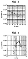
- Fig. 3 shows the relationship between Urbach energy Eu and ⁇ product of a photoconductive thin film formed on a glass substrate.
- a preferred range of the Urbach energy Eu measured by the constant photocurrent method (CPM) is 60 meV or below at 0.9 eV to 1.1 eV in the vicinity of 1.0 eV of photon energy.
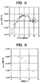
- Fig. 4 shows the relationship between hydrogen content C1 ascribable to Si-H bonds, hydrogen content C2 ascribable to Si-H 2 bonds and photoconductivity ⁇ product in the photoconductive thin film containing the present invention, formed on a silicon wafer.
- Solid black circles indicate those in as-depo state (a state after film formation and before irradiation by light), and marks x, those after 100-hour continuous irradiation by light of AM 1.5 (100 mW/cm 2 ).
- the C1/C2 and ⁇ product have a positive correlation.
- the ⁇ product is 10 -6 cm 2 /V or above, thus it is seen that the photoconductivity is good in that region.
- the ⁇ product little changes in the region where the C1/C2 is 0.8 or more, thus it is seen that light degradation little occurs.
- the Urbach energy Eu was also examined by CPM to find that Eu was 60 meV or below when the C1/C2 was 0.8 or more.
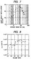
- Fig. 5 shows the relationship between C1+C2 and photoconductivity ⁇ product in the photoconductive thin film according to the present invention, formed on a silicon wafer.
- Solid black circles indicate those in as-depo state (a state after film formation and before irradiation by light), and marks x, those after 100-hour continuous irradiation by light of AM 1.5 (100 mW/cm 2 ).
- the ⁇ product is substantially 10 -6 cm 2 /V or above, thus it is seen that the photoconductivity is good in that region. Also, after irradiation by light, the ⁇ product is substantially 10 -6 cm 2 /V or above in the region where the C1+C2 is between 3% and 8%, showing little change before and after irradiation by light, thus it is seen that light degradation little occurs.
- the Urbach energy Eu was also examined by CPM to find that any Eu at 0.9 eV to 1.1 eV in the vicinity of 1.0 eV of photon energy was 60 meV or below in this region.
- a preferred relationship between the hydrogen content C1 atom% ascribable to Si-H bonds and the hydrogen content C2 atom% ascribable to Si-H 2 bonds is C1/C2 ⁇ 0.8 and 3 ⁇ C1+C2 ⁇ 8 atom%.
- crystal grains have an average grain diameter in the range of from about 5 nm to about 300 nm.
- a preferred range of the average grain diameter of the crystal grains is from 20 nm to 200 nm as calculated from the (220)-peak of silicon among X-ray diffraction peaks of the photoconductive thin film.
- the volume ratio has approximately been calculated from the resultant peak intensity ratios.
- the film may preferably be formed by plasma CVD making use of electromagnetic waves with a frequency of from 50 MHz to 900 MHz, using silicon-containing gas and hydrogen gas and at a pressure of from 10 mTorr to 500 mTorr and a substrate temperature of from 200°C to 600°C.
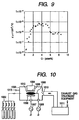
- Fig. 10 is a schematic view of an example of a system used in producing the photoconductive thin film according to the present invention.
- reference numeral 1002 denotes a material gas feed unit, which is constituted of gas cylinders, a pressure controller, mass-flow controllers, valves, feed lines and so forth.
- Reference numeral 1003 denotes a vacuum container; 1004, a heater for heating a substrate 1005; and 1006, an electrode A connected to a power source A (1007) and used to cause plasma 1012 to take place.
- Reference numeral 1008 denotes an electrode B for applying a bias to the plasma and is connected to a power source B (1009).
- Reference numeral 1010 denotes a conductance valve for controlling the pressure inside the vacuum container; and 1011, an exhaust system, where exhaust gas is led to an exhaust gas treatment equipment (not shown).
- Reference numeral 1013 denotes a pressure sensor which detects the pressure inside the vacuum container 1003.
- Its high-frequency power source may preferably be set at a frequency of from 50 to 900 MHz, and bias power source at a frequency of from 0 to 30 MHz.
- the pressure may preferably be set at from 10 to 500 mTorr, and substrate temperature at from 200 to 600°C.
- material gases silane (SiH 4 ), hydrogen (H 2 ), methane (CH 4 ), phosphine (PH 8 ) and boron fluoride (BF 3 ) may be used.
- an oil diffusion pump In the exhaust system, an oil diffusion pump, a turbo-molecular pump or a dry pump may be used.
- the production apparatus shown in Fig. 10 was used. Its power source A was set at a frequency of 100 MHz; the distance between the electrode A and the substrate, at 40 mm; and the power source B, at a frequency of 13.56 MHz.
- the electrode B was placed at a position intermediate between the electrode A and the substrate.
- an oil diffusion pump was used.
- material gases silane (SiH 4 ) and hydrogen (H 2 ) were used.
- As the substrate a glass plate of 5 cm x 5 cm and 1 mm thick was used.
- the photoconductive thin film formed was taken out to measure its absorption of light and Raman spectrum, and then an electrode was vacuum-deposited on the film to measure Urbach energy Eu by CPM and measure ⁇ product. From the Raman spectrum obtained, both wave-number shift at 480 (1/cm) and wave-number shift at 520 cm - 1 were seen, the former indicating amorphous silicon (a-Si) and the latter indicating crystalline silicon.
- the Urbach energy Eu at 0.9 eV to 1.1 eV in the vicinity of 1.0 eV of photon energy and the ⁇ product were as shown in Table 1. Observation of cross-sectional TEM images has revealed that crystal grains in the film have columnar shape.
- a photoconductive thin film was produced under conditions as shown in Table 1, changing the distance between the electrode A and the substrate to 100 mm, and measurement was made in the same manner as in Example 1. From the Raman spectrum obtained, both wave-number shift at 480 cm - 1 and wave-number shift at 520 (1/cm) were seen, the former indicating amorphous silicon (a-Si) and the latter indicating crystalline silicon.
- the Urbach energy Eu and the ⁇ product were as shown in Table 1. Incidentally, the crystal grains in the film had not especially a characteristic shape.
- the photoconductive thin film of Example 1 was found to have solar cell characteristics superior to those of Comparative Example 1.
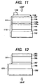
- the photovoltaic device shown in Fig. 11 (a p-i-n type solar cell) was produced. More specifically, this photovoltaic device is constituted of a back reflective layer 1103, a back transparent conductive layer 1104, a p-i-n junction layer 1111, a transparent conductive layer 1108 and a collector electrode 1109 which are superposed on a support 1102.
- a substrate 1110 is constituted of the support 1102, the back reflective layer 1103 and the back transparent conductive layer 1104. Stated specifically, used was a substrate comprising a support of a 5 cm x 5 cm and 1 mm thick stainless steel sheet, a 600 nm thick silver thin film formed thereon at a temperature of 300°C and a 2,500 nm thick zinc oxide (ZnO) further formed thereon by sputtering at 300°C. This substrate had a surface roughness Ra of 0.18 ⁇ m.
- the p-i-n junction layer is constituted of an n-type n1 layer 1105a, an n-type n2 layer 1105b, an i-type layer 1106 and a p-type layer 1107.
- the n-type n1 layer 1105a is formed as an a-Si:H:P thin film
- the n-type n2 layer 1105b as a ⁇ c-Si:H thin film
- the i-type layer 1106 as the photoconductive thin film of the present invention
- the p-type layer 1107 as a ⁇ c-Si:H:B thin film.
- a transparent conductive layer comprising ITO was formed by sputtering, and a comb collector electrode was further formed by EB (electron beam) vacuum deposition.
- Current and voltage characteristics (IV) of the solar cell thus produced was measured under a solar simulator (AM 1.5, 100 mW/cm 2 ), and solar cell characteristics (open-circuit voltage Voc, short-circuit photocurrent Jsc and conversion efficiency) were determined to obtain the results as shown in Table 2.
- Comparative Example 2 an i-type layer was formed under the same conditions as in Comparative Example 1, and a photovoltaic device was produced in the same manner as in Example 2. Measurement was made in the same manner as in Example 1 to obtain the results as shown in Table 2.
- the photovoltaic device of Example 2 was found to have solar cell characteristics superior to those of Comparative Example 2.
- the photovoltaic device shown in Fig. 12 (a p-i-n type solar cell) was produced.
- This photovoltaic device is a device of the type the light is received on the substrate side, and is constituted basically of a substrate 1210, a p-i-n junction layer 1211 and a back reflective layer 1203.
- the substrate 1210 is constituted of a transparent support 1202 formed of a glass plate and a transparent conductive layer 1208 formed of SnO 2 .
- the p-i-n junction layer 1211 is constituted of a p-type layer 1207 comprised of a ⁇ c-Si:H:B thin film, an i-type layer 1206 comprised of the photoconductive thin film of the present invention and an n-type layer 1205 comprised of an ⁇ c-Si:H:P thin film.
- the transparent conductive layer 1208 formed of SnO 2 was formed by sputtering, and the one having a surface-textured structure was used.
- the p-i-n junction layer was formed in the same manner as in Example 2.
- the i-type layer was formed in the same manner as in Example 1. Formation conditions for these are shown in Table 3.
- the photoconductive thin film of Example 3 was found to have superior solar cell characteristics.
- the photoconductive thin films of Examples 4a, 4c and 4d were found to have solar cell characteristics superior to those of the photoconductive thin film of Example 4b even under irradiation by light for a long time.
- a solar cell making use of the photoconductive thin film containing columnar crystal grains whose longer directions are substantially perpendicular to the substrate surface was produced.
- the same photovoltaic device as that of Example 2 was produced, except that the i-type layer was formed under conditions as shown in Table 5 [Table 5(A)-5(B)].
- Table 5(A)-5(B) After measurement of solar cell characteristics and Urbach energy Eu, cross-sectional TEM images in dark visual field were observed to examine the shape and direction of the crystal grains.
- the crystal grains had columnar shape, and their longer directions were substantially perpendicular to the substrate surface and at an average angle of 4.2° to the normal of the substrate.
- the crystal grains in the i-type layer of the photovoltaic device of Example 2 were also columnar crystal grains and their longer directions were substantially perpendicular to the substrate surface, but at an average angle of 8.2° to the normal of the substrate.
- the crystal grains in the i-type layer had not especially a characteristic shape.
- the photovoltaic devices having the photoconductive thin film containing columnar crystal grains whose longer directions are substantially perpendicular to the substrate surface were found to have superior solar cell characteristics.
- Photovoltaic devices making use of the photoconductive thin film of the present invention in which crystal grain region is in a volume ratio R of R ⁇ 0.5 was produced.
- Photovoltaic devices of Example 6a and 6b were produced in the same manner as in Example 2 except that their i-type layers were formed under conditions as shown in Table 6 [Table 6(A)-6(B)].
- Photovoltaic devices of Comparative Examples 3a and 3b were produced in the same manner as in Example 2 except that their i-type layers were formed under conditions as shown in Table 6, and measurement was made in the same manner as in Example 6. Results obtained are shown in Table 6.
- the photovoltaic devices of Examples 6a and 6b in which the crystal grain region is in a volume ratio R of R ⁇ 0.5 were found to cause little light degradation of solar cell characteristics even after continuous irradiation by strong light, compared with those of Comparative Examples 3a and 3b.
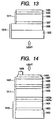
- a photovoltaic device (solar cell) having the cross-sectional structure as shown in Fig. 13 was produced.
- This photovoltaic device comprises a substrate 1310 and formed successively thereon a back reflective layer 1303, a photovoltaic p + -p - -n + junction layer 1311 and a transparent conductive layer 1308.
- a p + -type layer 1307 and an n + -type layer 1305 were formed under the same conditions as the p-type layer in Example 3 and the n-type layer in Example 4, respectively.
- a p - -type layer 1306 was formed under the same conditions as the i-type layer in Example 3 but, in addition thereto, boron fluoride (BF 3 ) was flowed at a rate of 0.6 sccm.
- Solar cell characteristics of the device obtained were measured to find that, like Example 3, it had superior characteristics.
- a single layer of the p - -type layer was also formed on a glass substrate and a comb electrode was further formed on the p - -type layer, to make measurement by CPM and measurement of conductivity activation energy.
- the Urbach energy Eu was found to be 55 meV.
- the activation energy was also found to be 0.42 eV and the conductivity type was confirmed to be p - -type.
- This photovoltaic device was also irradiated continuously for 500 hours by light of AM 1.5 (100 mW/cm 2 ) and thereafter the solar cell characteristics were again measured, where the solar cell characteristics little changed. Incidentally, observation of cross-sectional TEM images revealed that columnar crystal grains were present in the p - -type layer of Example 7.
- a photovoltaic device was produced, having the same structure as that of Example 7 except that the p - -type layer was replaced with an n - -type layer.
- the n - -type layer was formed under the same conditions as the i-type layer in Example 3 but, in addition thereto, phosphine (PH 3 ) was flowed at a rate of 0.3 sccm.
- Solar cell characteristics of the device obtained were measured to find that, like Example 3, it had superior characteristics.
- a single layer of the n - -type layer was also formed on a glass substrate and a comb electrode was further formed on the n - -type layer, to make measurement by CPM and measurement of conductivity activation energy.
- the Urbach energy Eu was found to be 54 meV.
- the activation energy was also found to be 0.39 eV and the conductivity type was confirmed to be n - -type.
- This photovoltaic device was also irradiated continuously for 500 hours by light of AM 1.5 (100 mW/cm 2 ) and thereafter the solar cell characteristics were again measured, where the solar cell characteristics little changed. Incidentally, observation of cross-sectional TEM images revealed that columnar crystal grains were present in the n - -type layer of Example 8.
- the photovoltaic device of the present invention was produced in which an additional p-i-n junction layer A is formed between the p-i-n junction layer and the transparent conductive layer and an i-type layer A constituting the p-i-n junction layer A is formed of amorphous silicon containing hydrogen. Its constitution is shown in Fig. 14.
- a substrate 1410 and a p-i-n junction layer 1411 are constituted in the same manner as the layers in Example 2. More specifically, the substrate 1410 is constituted of a support 1402, a back reflective layer 1403 and a back transparent conductive layer 1404. Stated specifically, used was a substrate comprising a support of a 5 cm x 5 cm and 1 mm thick stainless steel sheet, a 600 nm thick silver thin film formed thereon at a temperature of 300°C and a 2,500 nm thick zinc oxide (ZnO) further formed thereon by sputtering at 300°C. This substrate had a surface roughness Ra of 0.18 ⁇ m.
- the p-i-n junction layer is constituted of an n-type n1 layer 1405a, an n-type n2 layer 1405b, an i-type layer 1406 and a p-type layer 1407.
- the n-type n1 layer 1405a is formed as an a-Si:H:P thin film
- the n-type n2 layer 1405b as a ⁇ c-Si:H thin film
- the i-type layer 1406 as the photoconductive thin film of the present invention
- the p-type layer 1407 as a ⁇ c-Si:H:B thin film.
- the additional p-i-n junction layer A 1421 formed between the p-i-n junction layer and the transparent conductive layer 1408 is constituted of an n-type layer A 1425 comprised of an amorphous silicon thin film (a-Si:H:P), an i-type layer A 1426 comprised of an amorphous silicon thin film (a-Si:H) and a p-type layer A 1427 comprised of a microcrystalline silicon thin film ( ⁇ c-Si:H:B).
- the photovoltaic device of the present invention was found to have superior heat resistance. Measurement by CPM was made on a single layer formed under the conditions for the i-type layer and on which a comb electrode was formed by vacuum deposition. Observation of cross-sectional TEM images revealed that columnar crystal grains were present in the i-type layer of Example 9.
- Temperature of photovoltaic devices was changed from 25°C to 90°C, and their conversion efficiency was measured to determine temperature characteristics of conversion efficiency.
- the temperature characteristics of conversion efficiency of the photovoltaic device of Example 9 were -0.035%/°C.
- the temperature characteristics of conversion efficiency of the photovoltaic device of Example 2 were -0.046%/°C
- the temperature characteristics of conversion efficiency of the photovoltaic device of Comparative Example 2 were -0.052%/°C. From these facts, the temperature characteristics of conversion efficiency of the photovoltaic device of Example 9 were found to be improved reasonably, compared with those of Example 2 and Comparative Example 2.
- Example 9 The procedure of Example 9 was repeated except that the i-type layer formed therein was formed under the conditions as shown in Table 7 and the transparent conductive layer 1408 was formed by EB vacuum deposition. Measurement was made in the same manner to obtain the results as shown together in Table 7.
- the photovoltaic device of Example 9 was found to have solar cell characteristics and heat resistance superior to those of Comparative Example 4.
- Example 9 Layer formation was carried out under the same conditions as in Example 9 except that, when the i-type layer was formed therein, phosphine gas was flowed at a rate of 0.1 sccm. Observation of cross-sectional TEM images revealed that columnar crystal grains were present in the film of this layer. Measurement of solar cell characteristics and heat resistance test were also made similarly to find that the photovoltaic device obtained had superior solar cell characteristics and heat resistance like those in Example 9.
- a photovoltaic device was produced whose back transparent conductive layer has a surface roughness Ra of 0.35 ⁇ m.
- the photovoltaic device was produced in the same manner as in Example 2 except that the back transparent conductive layer was formed in a layer thickness of 4,000 nm at a temperature of 350°C.
- a photovoltaic device was produced in which a copper magnesium (Cu 2 Mg) layer formed by DC magnetron sputtering at 300°C was used as the back reflective layer.
- the photovoltaic device was produced under the same layer formation conditions as in Example 2 except that the silver was replaced with the above copper magnesium. After its solar cell characteristics were measured, the device was left in an environment of a high temperature of 85°C and a high humidity of 85% for 150 hours while applying a reverse bias of -1 V to the collector electrode, which was then restored to an environment of normal temperature to measure its solar cell characteristics. As a result, the characteristics were seen to little lower.
- a photovoltaic device was produced under the same constitution and conditions as in Example 9 except that, when the i-type layer A was formed therein, methane gas (CH 4 ) was flowed at a rate of 3 sccm.
- the optimum operating voltage and optimum operating electric current of this photovoltaic device were 1.05 times and 0.91 time those of the photovoltaic device of Example 9, respectively. Its conversion efficiency was 0.96 time the same, but, when photovoltaic devices were connected in series to provide a module, the comb electrode was able to be narrowed correspondingly to the operating electric current which was able to be made lower. It was also possible to reduce the power loss due to sheet resistance of the transparent conductive layer.
- the photoconductive thin film of the present invention has a superior photoconductivity and causes little light degradation.
- the photovoltaic device making use of the photoconductive thin film of the present invention has superior open-circuit voltage, short-circuit photocurrent and photoelectric conversion efficiency and causes little light degradation.
- the tandem type photovoltaic device according to the present invention also has superior open-circuit voltage, short-circuit photocurrent and photoelectric conversion efficiency, causes little light degradation, and also have superior heat resistance and temperature characteristics.
- any expensive gas such as germane need not be used, the photovoltaic device can be made low-cost.
- This film provides a photoconductive thin film free of light degradation and having superior photoconductivity, and provides a photovoltaic device having superior temperature characteristics and long-term stability.
Landscapes
- Photovoltaic Devices (AREA)
- Physical Vapour Deposition (AREA)
Applications Claiming Priority (2)
| Application Number | Priority Date | Filing Date | Title |
|---|---|---|---|
| JP3345498 | 1998-02-17 | ||
| JP3345498 | 1998-02-17 |
Publications (2)
| Publication Number | Publication Date |
|---|---|
| EP0936681A2 true EP0936681A2 (de) | 1999-08-18 |
| EP0936681A3 EP0936681A3 (de) | 1999-09-08 |
Family
ID=12386994
Family Applications (1)
| Application Number | Title | Priority Date | Filing Date |
|---|---|---|---|
| EP99103051A Withdrawn EP0936681A3 (de) | 1998-02-17 | 1999-02-16 | Fotoleitende Dünnschicht und diese Dünnschicht anwendende photovoltaische Vorrichtung |
Country Status (4)
| Country | Link |
|---|---|
| US (1) | US6215061B1 (de) |
| EP (1) | EP0936681A3 (de) |
| JP (1) | JPH11317538A (de) |
| CN (2) | CN100364115C (de) |
Cited By (1)
| Publication number | Priority date | Publication date | Assignee | Title |
|---|---|---|---|---|
| EP1241712A3 (de) * | 2001-03-15 | 2004-12-15 | Canon Kabushiki Kaisha | Dünnschichtige polykristalline Solarzelle und Herstellungsverfahren |
Families Citing this family (18)
| Publication number | Priority date | Publication date | Assignee | Title |
|---|---|---|---|---|
| JP3437386B2 (ja) * | 1996-09-05 | 2003-08-18 | キヤノン株式会社 | 光起電力素子、並びにその製造方法 |
| JP2002222976A (ja) * | 2001-01-29 | 2002-08-09 | Kyocera Corp | 光電変換装置 |
| US7189917B2 (en) * | 2003-03-26 | 2007-03-13 | Canon Kabushiki Kaisha | Stacked photovoltaic device |
| JP2004296693A (ja) * | 2003-03-26 | 2004-10-21 | Canon Inc | 積層型光起電力素子および電流バランス調整方法 |
| JP2004335823A (ja) * | 2003-05-09 | 2004-11-25 | Canon Inc | 光起電力素子及び光起電力素子の形成方法 |
| US20070170462A1 (en) * | 2006-01-26 | 2007-07-26 | Fronted Analog And Digital Technology Corporation | Photo sensor and preparation method thereof |
| CN102347402A (zh) * | 2006-06-23 | 2012-02-08 | 夏普株式会社 | 等离子体处理装置、等离子体处理方法及光电转换元件 |
| US20090293954A1 (en) * | 2008-05-30 | 2009-12-03 | Semiconductor Energy Laboratory Co., Ltd. | Photoelectric Conversion Device And Method For Manufacturing The Same |
| US8535760B2 (en) * | 2009-09-11 | 2013-09-17 | Air Products And Chemicals, Inc. | Additives to silane for thin film silicon photovoltaic devices |
| DE102009042018A1 (de) * | 2009-09-21 | 2011-03-24 | Fraunhofer-Gesellschaft zur Förderung der angewandten Forschung e.V. | Solarzelle |
| TWI430491B (zh) * | 2010-12-31 | 2014-03-11 | Au Optronics Corp | 堆疊式太陽能電池模組 |
| TWI425690B (zh) * | 2010-12-31 | 2014-02-01 | 友達光電股份有限公司 | 堆疊式太陽能電池模組 |
| US8895435B2 (en) * | 2011-01-31 | 2014-11-25 | United Microelectronics Corp. | Polysilicon layer and method of forming the same |
| US20130019929A1 (en) * | 2011-07-19 | 2013-01-24 | International Business Machines | Reduction of light induced degradation by minimizing band offset |
| JP5925634B2 (ja) * | 2011-08-18 | 2016-05-25 | 株式会社半導体エネルギー研究所 | 半導体の欠陥評価方法 |
| KR20130136739A (ko) * | 2012-06-05 | 2013-12-13 | 엘지이노텍 주식회사 | 태양전지 및 이의 제조방법 |
| JP6773944B2 (ja) * | 2016-01-06 | 2020-10-21 | inQs株式会社 | 光発電素子 |
| CN112968076A (zh) * | 2021-03-30 | 2021-06-15 | 深圳第三代半导体研究院 | 一种透明导电薄膜的制备方法 |
Family Cites Families (3)
| Publication number | Priority date | Publication date | Assignee | Title |
|---|---|---|---|---|
| JP2756050B2 (ja) * | 1992-03-03 | 1998-05-25 | キヤノン株式会社 | 光起電力装置 |
| JPH0794766A (ja) * | 1993-09-21 | 1995-04-07 | Kanegafuchi Chem Ind Co Ltd | 薄膜多結晶シリコン光電変換装置及びその製造方法 |
| JPH08116080A (ja) * | 1994-10-19 | 1996-05-07 | Sharp Corp | 薄膜太陽電池およびその製造方法 |
-
1999
- 1999-02-12 JP JP11033643A patent/JPH11317538A/ja active Pending
- 1999-02-15 CN CNB2004100617991A patent/CN100364115C/zh not_active Expired - Fee Related
- 1999-02-15 CN CNB991029410A patent/CN1244163C/zh not_active Expired - Fee Related
- 1999-02-16 EP EP99103051A patent/EP0936681A3/de not_active Withdrawn
- 1999-02-16 US US09/250,246 patent/US6215061B1/en not_active Expired - Lifetime
Non-Patent Citations (4)
| Title |
|---|
| MEIER, J. ET AL.: "On the way towards high efficiency thin film silicon solar cells by the "micromorph" concept" AMORPHOUS SILICON TECHNOLOGY- 1996 MAT. RES. SOC. SYMP. PROC., vol. 420, 8 - 12 April 1996, pages 3-14, XP002108941 S. Francisco * |
| RUSSEL, E. ET AL.: "Deposition of polycrystalline silicon thin films by plasma enhanced CVD" MICROCRYSTALLINE SEMICONDUCTORS: MATERIALS SCIENCE & DEVICES, MAT. RES. SOC. SYMP. PROC., vol. 283, 30 November 1992 (1992-11-30) - 4 December 1992 (1992-12-04), pages 659-664, XP002108942 Boston * |
| TZOLOV, M. ET AL.: "Optical and transport properties on thin microcrystalline silicon films prepared by very high frequency glow discharge for solar cell applications" J. APPL. PHYS.,1 June 1997 (1997-06-01), pages 7376-7385, XP002108943 * |
| VANECEK, M. ET AL.: "Optical properties of microcrystalline materials" PROCEEDINGS OF THE SEVENTEENTH INTERNATIONAL CONFERENCE ON AMORPHOUS AND MICROCRYSTALLINE SEMICONDUCTORS, 25 - 29 August 1997, pages 967-972, XP002108940 Budapest * |
Cited By (1)
| Publication number | Priority date | Publication date | Assignee | Title |
|---|---|---|---|---|
| EP1241712A3 (de) * | 2001-03-15 | 2004-12-15 | Canon Kabushiki Kaisha | Dünnschichtige polykristalline Solarzelle und Herstellungsverfahren |
Also Published As
| Publication number | Publication date |
|---|---|
| EP0936681A3 (de) | 1999-09-08 |
| US6215061B1 (en) | 2001-04-10 |
| CN1244163C (zh) | 2006-03-01 |
| JPH11317538A (ja) | 1999-11-16 |
| CN1560927A (zh) | 2005-01-05 |
| CN100364115C (zh) | 2008-01-23 |
| CN1228617A (zh) | 1999-09-15 |
Similar Documents
| Publication | Publication Date | Title |
|---|---|---|
| US6215061B1 (en) | Photoconductive thin film, and photovoltaic device making use of the same | |
| US7030313B2 (en) | Thin film solar cell and method of manufacturing the same | |
| AU734676B2 (en) | Photovoltaic element and method of producing same | |
| US5913986A (en) | Photovoltaic element having a specific doped layer | |
| US6835888B2 (en) | Stacked photovoltaic device | |
| JP2695585B2 (ja) | 光起電力素子及びその製造方法、並びにそれを用いた発電装置 | |
| AU2005200023B2 (en) | Photovoltaic device | |
| US20110126893A1 (en) | Thin film silicon solar cell and manufacturing method thereof | |
| US5676765A (en) | Pin junction photovoltaic device having a multi-layered I-type semiconductor layer with a specific non-single crystal I-type layer formed by a microwave plasma CVD process | |
| US5849108A (en) | Photovoltaic element with zno layer having increasing fluorine content in layer thickness direction | |
| JP2008153646A (ja) | 半導体素子の製造方法 | |
| EP1056139A2 (de) | Photoelektrische Umwandlungsvorrichtung und Herstellungsverfahren | |
| US5419783A (en) | Photovoltaic device and manufacturing method therefor | |
| US5284525A (en) | Solar cell | |
| US5242505A (en) | Amorphous silicon-based photovoltaic semiconductor materials free from Staebler-Wronski effects | |
| US5104455A (en) | Amorphous semiconductor solar cell | |
| Miyajima et al. | Highly conductive microcrystalline silicon carbide films deposited by the hot wire cell method and its application to amorphous silicon solar cells | |
| Inthisang et al. | Fabrication of high open‐circuit voltage a‐Si1–xOx: H solar cells by using p‐a‐Si1–xOx: H as window layer | |
| Kenne et al. | High deposition rate preparation of amorphous silicon solar cells by rf glow discharge decomposition of disilane | |
| JP2004146735A (ja) | シリコン光起電力素子及びその製造方法 | |
| JP2004253417A (ja) | 薄膜太陽電池の製造方法 | |
| JPH06318719A (ja) | 光起電力素子 | |
| JPH05299676A (ja) | 太陽電池 | |
| AU7211601A (en) | Method of producing a microcrystal semiconductor thin film | |
| WO2012113441A1 (en) | Thin-film solar fabrication process, deposition method for a layer stack of a solar cell, and solar cell precursor |
Legal Events
| Date | Code | Title | Description |
|---|---|---|---|
| PUAI | Public reference made under article 153(3) epc to a published international application that has entered the european phase |
Free format text: ORIGINAL CODE: 0009012 |
|
| PUAL | Search report despatched |
Free format text: ORIGINAL CODE: 0009013 |
|
| AK | Designated contracting states |
Kind code of ref document: A2 Designated state(s): CH DE ES FR GB IT LI NL SE |
|
| AX | Request for extension of the european patent |
Free format text: AL;LT;LV;MK;RO;SI |
|
| AK | Designated contracting states |
Kind code of ref document: A3 Designated state(s): AT BE CH CY DE DK ES FI FR GB GR IE IT LI LU MC NL PT SE |
|
| AX | Request for extension of the european patent |
Free format text: AL;LT;LV;MK;RO;SI |
|
| 17P | Request for examination filed |
Effective date: 20000125 |
|
| AKX | Designation fees paid |
Free format text: CH DE ES FR GB IT LI NL SE |
|
| 17Q | First examination report despatched |
Effective date: 20060911 |
|
| STAA | Information on the status of an ep patent application or granted ep patent |
Free format text: STATUS: THE APPLICATION HAS BEEN WITHDRAWN |
|
| 18W | Application withdrawn |
Effective date: 20070316 |