EP0936637B1 - Transformator - Google Patents
Transformator Download PDFInfo
- Publication number
- EP0936637B1 EP0936637B1 EP99101568A EP99101568A EP0936637B1 EP 0936637 B1 EP0936637 B1 EP 0936637B1 EP 99101568 A EP99101568 A EP 99101568A EP 99101568 A EP99101568 A EP 99101568A EP 0936637 B1 EP0936637 B1 EP 0936637B1
- Authority
- EP
- European Patent Office
- Prior art keywords
- transformer
- parts
- core
- chamber system
- chambers
- Prior art date
- Legal status (The legal status is an assumption and is not a legal conclusion. Google has not performed a legal analysis and makes no representation as to the accuracy of the status listed.)
- Expired - Lifetime
Links
- 238000004804 winding Methods 0.000 claims description 47
- 239000004020 conductor Substances 0.000 claims description 40
- 238000000034 method Methods 0.000 claims description 11
- 238000002955 isolation Methods 0.000 claims description 8
- 238000009413 insulation Methods 0.000 claims description 6
- 239000004033 plastic Substances 0.000 claims description 5
- 230000013011 mating Effects 0.000 claims description 3
- 238000001465 metallisation Methods 0.000 claims description 3
- 229920001169 thermoplastic Polymers 0.000 claims description 3
- 239000004416 thermosoftening plastic Substances 0.000 claims description 3
- RYGMFSIKBFXOCR-UHFFFAOYSA-N Copper Chemical compound [Cu] RYGMFSIKBFXOCR-UHFFFAOYSA-N 0.000 description 10
- 229920000106 Liquid crystal polymer Polymers 0.000 description 7
- 239000004977 Liquid-crystal polymers (LCPs) Substances 0.000 description 7
- 229910052802 copper Inorganic materials 0.000 description 7
- 239000010949 copper Substances 0.000 description 7
- 238000009713 electroplating Methods 0.000 description 4
- 238000004519 manufacturing process Methods 0.000 description 3
- 238000005476 soldering Methods 0.000 description 3
- KDLHZDBZIXYQEI-UHFFFAOYSA-N Palladium Chemical compound [Pd] KDLHZDBZIXYQEI-UHFFFAOYSA-N 0.000 description 2
- 230000004913 activation Effects 0.000 description 2
- 230000000694 effects Effects 0.000 description 2
- 238000001746 injection moulding Methods 0.000 description 2
- 229920002799 BoPET Polymers 0.000 description 1
- 239000005041 Mylar™ Substances 0.000 description 1
- 239000000853 adhesive Substances 0.000 description 1
- 230000001070 adhesive effect Effects 0.000 description 1
- 230000008878 coupling Effects 0.000 description 1
- 238000010168 coupling process Methods 0.000 description 1
- 238000005859 coupling reaction Methods 0.000 description 1
- 238000011161 development Methods 0.000 description 1
- 230000018109 developmental process Effects 0.000 description 1
- 238000005516 engineering process Methods 0.000 description 1
- 238000005530 etching Methods 0.000 description 1
- 238000010438 heat treatment Methods 0.000 description 1
- 239000000463 material Substances 0.000 description 1
- 229910052751 metal Inorganic materials 0.000 description 1
- 239000002184 metal Substances 0.000 description 1
- 229910052763 palladium Inorganic materials 0.000 description 1
- 229920003223 poly(pyromellitimide-1,4-diphenyl ether) Polymers 0.000 description 1
- 238000004064 recycling Methods 0.000 description 1
- 238000000926 separation method Methods 0.000 description 1
- 229910000679 solder Inorganic materials 0.000 description 1
- 230000009466 transformation Effects 0.000 description 1
Images


Classifications
-
- H—ELECTRICITY
- H01—ELECTRIC ELEMENTS
- H01F—MAGNETS; INDUCTANCES; TRANSFORMERS; SELECTION OF MATERIALS FOR THEIR MAGNETIC PROPERTIES
- H01F27/00—Details of transformers or inductances, in general
- H01F27/28—Coils; Windings; Conductive connections
- H01F27/32—Insulating of coils, windings, or parts thereof
- H01F27/324—Insulation between coil and core, between different winding sections, around the coil; Other insulation structures
-
- H—ELECTRICITY
- H01—ELECTRIC ELEMENTS
- H01F—MAGNETS; INDUCTANCES; TRANSFORMERS; SELECTION OF MATERIALS FOR THEIR MAGNETIC PROPERTIES
- H01F27/00—Details of transformers or inductances, in general
- H01F27/34—Special means for preventing or reducing unwanted electric or magnetic effects, e.g. no-load losses, reactive currents, harmonics, oscillations, leakage fields
-
- H—ELECTRICITY
- H01—ELECTRIC ELEMENTS
- H01F—MAGNETS; INDUCTANCES; TRANSFORMERS; SELECTION OF MATERIALS FOR THEIR MAGNETIC PROPERTIES
- H01F27/00—Details of transformers or inductances, in general
- H01F27/28—Coils; Windings; Conductive connections
- H01F27/2804—Printed windings
Definitions
- the invention is based on a transformer comprising a primary winding and at least one secondary winding, which are arranged in the form of conductor tracks on one or more layers of a flat carrier, in particular films or printed circuit boards.
- Transformers of this type are used for example in switched-mode power supplies having very high switching frequencies, in particular frequencies of more than 50 kHz, thereby enabling the transformer to be kept very small.
- FIGS 1a, 1b Known transformers of this type, illustrated in Figures 1a, 1b, contain for example a core with two core parts K1, K2, primary and secondary windings W1, W2 being arranged in the openings therein.
- the windings are arranged as conductor tracks L on non-conductive layers F of a flat carrier, a plurality of layers in each case lying one above the other, depending on the number of turns required.
- a plurality of layers P are in this case serially interconnected by plated-through holes T2 and have two external terminals T1, T3.
- the outer and inner edges R of the layers P must remain free, in other words are not permitted to have any conductor tracks.
- the conductor tracks L are produced as copper tracks on the layers P using etching technology, for example.
- Figures 1a, 1b are sectional drawings corresponding to a central horizontal and a central vertical plane of the transformer.
- a Transformer according to the preamble of claim 1 is disclosed in WO 91/15861.
- the object of the present invention is to specify a compact transformer of the type mentioned in the introduction which has improved electrical properties.
- the transformer comprises a coil former with a chamber system having chambers which accommodate the layers with the windings.
- the windings are arranged in at least two separate chambers, thereby producing long distances for creepage currents between the windings without the transformer having to be potted.
- the chamber system is formed by at least two parts, which are formed in such a way that chambers are produced by mating of these parts.
- the chamber system can, for example, be formed by two parts, whose shape in each case corresponds to an asymmetrical H in cross section and which are mated in such a way as to produce one closed chamber in the region of a core opening for the secondary winding and two adjacent, open chambers for the primary winding.
- the chamber system is formed by three parts, two parts being placed onto a central part in such a way as to produce two closed chambers, one for in each case one winding.
- the parts of the chamber system may be produced for example from injection-moulded thermoplastic, and their dimensions are chosen in such a way that they latch together with one another in the course of mating at the outer walls.
- the outer walls may lie one above the other like a sandwich, thereby producing long distances for creepage currents without necessitating any increase in the space required by the chamber system.
- the chamber system surrounds, in particular, the regions and the openings of the core and is open on both sides, with the result that the layers with the windings can be routed out on both sides in order to make contact with terminals and for effecting contacts between different layers.
- the outer part of the chamber system is provided with an extension on its outer edge, with the result that the mated parts assume the shape of an H in a section via the core, as a result of which the creepage path is enlarged at these edges.
- the layers themselves may be sufficiently enlarged at the open sides, as previously, with the result that the safety regulations are likewise adhered to here.
- the contact-making by the chamber system is not restricted as a result of this.
- the parts of the chamber system themselves take up part of the space in the openings in the core, this is compensated for since the conductor tracks now extend over the entire width of a layer up to the walls of the chamber system.
- the utilizable copper area is increased by approximately 45% for a transformer with a transformation power of approximately 140 watts.
- the electrical power loss is reduced in the same ratio.
- the chambers serve as an assembly aid and reduce the variation in the geometry and, consequently, in the electrical properties on account of assembly tolerances.
- the power of the transformer can be increased as a result of this or the size of the transformer can be reduced with a predetermined power.
- the layers are, for example, printed circuit boards or films, for example Mylar or Kapton films.
- the chamber system therefore has, according to the invention, webs with metallized slots which establish connections between conductor tracks which are arranged on the top side and the underside of a carrier layer coated on both sides, or between conductor tracks of two adjacent carrier layers.
- a slot in this case encompasses, like a clamp to a certain extent, the edge of a carrier layer coated on both sides and thereby connects two conductor tracks, in the case of which, for example, one end in each case is led up to this edge.
- the webs of the chamber system and the metallized slots can be produced by the two-shot MID ("moulded interconnect devices") process together with the chamber parts.
- the MID process a plastic injection-moulding process, makes it possible to produce filigree structures made of thermoplastics together with metallic conductor tracks, which can replace conventional printed circuit boards.
- the webs are in this case selectively metallized for the production of the slots.
- the metallized slots may additionally be strengthened by electroplating.
- electroplating it is possible to provide a solder-paste application with a downstream soldering operation.
- the contacts are distributed between two or more webs in order to ensure an interspace having a sufficient insulation spacing between two slots.
- activation by means of palladium nuclei can be used in the first shot, for example, the said activation improving the adhesion of a subsequently applied copper layer.
- the carrier layers it is possible to use, in particular, an LCP (Liquid Crystal Polymer) structure to which conductor tracks can be applied using the Futuron process, for example.
- LCP Liquid Crystal Polymer
- the LCP film is highly temperature-resistant, thereby enabling soldering processes, for example the Reflow process, to be used for the chamber system with the carrier layers arranged therein.
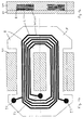
- the transformer illustrated in Figure 2a contains a core having two core parts K1, K2 in the form of an E/E core, the turns of a primary winding W1 and of at least one secondary winding W2 leading through the openings in the said core.
- the windings W1, W2 are in this case arranged in a chamber system composed of three parts P1, P2, P3 in such a way that two closed chambers C1, C2 are produced in the region of the sectional plane, the windings W1, W2 being arranged separately from one another in the said chambers.
- One of the parts P2 has the shape of a double-T, referring to an opening, and the other two parts P1, P3 have the shape of a U.
- the two parts P1, P3 are produced to fit with the central part P2 and are mated with the latter to produce the closed chambers C1, C2.
- the U-shaped parts P1, P2 are seated within the T-shaped part P2.
- Long creepage paths are produced between the two windings W1 and W2 on account of the double-T of the part P2 arranged in the centre.
- the windings W1, W2 are constructed from a plurality of wrappings of carrier layers F, between which an insulating layer is arranged.
- the carrier layers F are provided with conductor tracks on both sides. Carrier layers coated on one side can likewise be used, however.
- An exemplary arrangement of a conductor track L on the carrier layer F can be seen in Figure 2b, where five turns are arranged on one side with a contact T1 at the beginning and a contact T2 at the end of the conductor track.
- the end of the conductor track T2 is routed via a plated-through hole to the underside of the carrier layer F, on which turns are likewise arranged, and is routed back to the top side again by means of a plated-through hole T3.
- Figure 2b illustrates the transformer of Figure 2a in a sectional plane perpendicular to the sectional plane of Figure 2a, the sectional plane passing through the core part K1.
- the layers F and the chamber system with the parts P1, P2 completely fill the openings in the core K1.
- the chambers of the chamber system are completely closed in the region of the openings in the core and in the core, and only at the two sides on the left and right are the layers F with the conductors L routed out from the chambers C1, C2 for the terminals of the windings W1, W2.
- the terminals T1, T3 of one winding W1 are located, for example, on the left-hand side and the terminals of the other winding W2 are then located oppositely on the right-hand side, thereby ensuring a sufficient spacing for mains power supply isolation.
- the double-T-shaped part P2 additionally contains an extension P2L at its edges, for the purpose of enlarging the creepage paths in this region. This arrangement makes it possible for the conductor tracks L to extend over the entire width of the layer F in the region of the core openings.
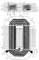
- Figures 3a, 3b illustrate a transformer with a chamber system containing an inner part P4 and an outer part P5, which form a closed chamber C4 and two open chambers C3, C5.
- the two parts P4, P5 have the shape of an asymmetrical H, with a slightly different size, so that one can be placed into the other.
- This makes it possible to arrange the secondary winding W2 in the closed, central chamber C4 and the primary winding W1, divided into two halves, in the two outer chambers C3, C5.
- the arrangement of the primary winding W1 in the central chamber C4 and of the secondary winding W2 in the two outer chambers C3, C5 is also possible.
- the shape of the outer walls like an asymmetrical H means that long creepage paths between the windings W1 and W2 are likewise obtained in this case.
- Figure 3b shows the transformer of Figure 3a in a sectional plane corresponding to that of Figure 2b.
- the conductor tracks L of a layer F are likewise extended completely over the width of the inner chamber of the part P5.
- the chamber system having the parts P4 and P5 is likewise closed only in the region in the core and around the openings therein, and open on both sides for the contact-making of the terminals T1 and T3.
- the thickness of the walls of the chamber parts P4 and P5 can be kept very small, for example 0.4 mm.
- the carrier layers F may protrude from the chamber system outside the openings in the core parts K1, K2, as described above, for example in order to perform contact-making at the terminals T1 and T3.
- the required insulation spacing can be produced here, without any disadvantages, by a sufficient edge R on the carrier layer F.
- the transformer can be used for example in a switched-mode power supply, in which the primary winding W1 is connected to a switching transistor and, via a bridge rectifier, to the mains power supply.
- a plurality of secondary windings for supplying loads can be arranged both on the secondary side with mains power supply isolation and on the primary side without mains power supply isolation.
- the mains power supply isolation proceeds on the circuit board on which the transformer is arranged in a device, underneath its core.
- the question of whether this secondary winding is provided with mains power supply isolation or no mains power supply isolation depends on whether the terminals of a secondary winding are routed out towards the left or towards the right.
- the windings can be distributed in a corresponding manner between the chambers of the chamber system. However, other configurations, in particular with other core shapes, are likewise possible.
- the chamber system contains webs S with metallized slots N, illustrated in Figure 4, which establish connections between conductors L on the top side and the underside of the carrier layers F.
- the webs S are arranged on chamber walls PK, which rise vertically from the bottom part B of a chamber part in this exemplary embodiment.
- the slots N may be designed such that they are trough-shaped, as in this exemplary embodiment, or notched, with the result that the carrier layers F latch into place with an edge.
- a metallized slot N surrounds the edge like a clamp and thereby establishes electrical contact between a conductor track L on the top side and a conductor track L on the underside of the relevant carrier layer F.
- the depth of the slot may have values in the region of 0.5 mm, for example.
- the carrier layer that is used may be, in particular, an LCP structure having a thickness of 0.05 mm, which can be provided with conductor tracks having a thickness of 35 ⁇ m or 70 ⁇ m.
- a solder-paste application LP which is introduced into the slots N. Appropriate heating, for example in a Reflow process, enables the solder paste to fuse with the conductor tracks L and the metallization layer of the slot N.
- a conductive adhesive may also be used instead of this soldering process.
- Insulating layers IS are arranged between the carrier layers F, in order to avoid short circuits between conductor tracks.
- the webs S contain a metallized slot N only for every second carrier layer F, thereby producing a sufficient insulation spacing between two slots.
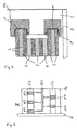
- Figure 5a illustrates an inner chamber part P4 in a plan view, into which chamber part the carrier layers F, for example the secondary winding W2, are inserted in the form of a stack.
- the inner chamber part contains a bottom part B, on which the bottommost carrier layer F bears in as planar a manner as possible, and side walls PK, which determine the width of the carrier layers.
- This chamber part P4 can be used for an E/E core, for example, the central core limb of the core passing through the opening OE in the chamber part P4.
- the winding arranged in the chamber part P4 is completely enclosed, in the region of the core and the openings therein, by a second chamber part, not illustrated, thereby making it possible to use the entire width between the chamber walls PK for conductor tracks on the carrier layers F.
- the chamber part P4 and the associated, terminating outer chamber part are similar to the chamber parts P4 and P5 of Figure 3a, but have lateral extensions. As a result of this, it is possible to arrange further webs in the inner chamber part P4, the webs S1, S2 and S5, S6 in the exemplary embodiment of Figure 5a.
- the webs S3 and S4 can also be processed from the side through a cutout AS.
- FIG. 5b shows a view of the chamber part P4 in the section A-B.
- Metallized slots N1-N5 have been worked into these webs S3, S4, which slots in each case establish contact between a conductor track on the top side and the underside of a carrier layer. Since the slots N1-N5 are distributed between two webs, a sufficient insulation space in between the slots is produced. As a result of this, one web is used in each to effect contact with next-but-one carrier layers, with the result that two webs are sufficient. For example, upper and lower conductor tracks of five carrier layers make contact with one another by means of the five slots N1-N5, in order to avoid plated-through holes.
- the webs S3, S4 only establish contacts of conductor tracks on the top side and underside of carrier layers, in order to avoid plated-through holes. Contacts between carrier layers can likewise be established by the invention but, in this embodiment, are intended to be realized on the outer edge of the carrier layers together with the terminals of the winding.
- FIG 6 illustrates the slots N1-N5 of the webs S3, S4 in an enlarged manner in a detail drawing.
- a copper structure KS which is not present in Figure 5b, can additionally be seen here. This copper structure effects electrical connection to the slots N1-N5, by means of which the metallization of the slots N1-N5 can be reinforced by electroplating in a copper bath during production. The copper track KS is removed again after the electroplating. The copper layer KS can be applied directly on the wall PK.
- the transformer has improved electrical properties due to better utilization of the core openings.
- the chamber system which has been explained with reference to Figures 2-6 relates essentially to an E/E core or E/I core.
- Transformers of this type may be used for example in resonant converter switched-mode power supplies which provide relatively high power outputs in the region of considerably more than 100 watts, for example for plasma television sets or television sets having large picture tubes.
Landscapes
- Engineering & Computer Science (AREA)
- Power Engineering (AREA)
- Coils Or Transformers For Communication (AREA)
- Coils Of Transformers For General Uses (AREA)
Claims (11)
- Transformator mit einem Kern (K1, K2), einer primären Wicklung (W1) und mindestens einer sekundären Wicklung (W2), die als Leiterbahnen (L) auf einer oder mehreren Schichten (F) eines flachen Trägers angeordnet sind,
wobei der Transformator einen Spulenkörper mit Kammersystem (P1 - P5) enthält, das die Trägerschichten (F) mit den Wicklungen (W1, W2) aufnimmt, und das Kammersystem mindestens zwei Kammern (C1 - C5) enthält, in denen die Wicklungen (W1, W2) angeordnet sind, wobei die primäre und die sekundäre Wicklung (W1, W2) in verschiedenen Kammern angeordnet sind,
dadurch gekennzeichnet, daß
Stege (S) mit einer metallisierten Nut (N) in dem Kammersystem (P4) angeordnet sind, um einen Kontakt mit den Leiterbahnen (L) zu bilden, dass die Stege (S) Verbindungen zwischen Leiterbahnen (L) bilden, die an der Oberseite und der Unterseite einer doppelseitigen Trägerschicht (F) angeordnet sind, und/oder Bildung von Verbindungen zwischen den Leiterbahnen (L) von zwei verschiedenen Trägerschichten (F). - Transformator nach Anspruch 1, dadurch gekennzeichnet, daß der Spulenträger wenigstens zwei Teile (P1 - P5) enthält, die derart geformt sind, daß durch Zusammenstecken der Teile (P1, P2, P3; P4, P5) mindestens zwei Kammern (C1, C2; C3 - C5) entstehen, und daß wenigstens eine der Kammern (C1- C5) zumindest in den Bereich des Kerns geschlossen ist.
- Transformator nach Anspruch 2, dadurch gekennzeichnet, daß zwei Teile (P4, P5) derart zusammengesteckt sind, daß eine innere Kammer (C4) entsteht, die in dem Bereich des Kernes (K1, K2) geschlossen ist für die Sekundärwicklung (W1) und zwei benachbarte offene Kammern (C3, C5) für die Primärwicklung (W2).
- Transformator nach Anspruch 2, dadurch gekennzeichnet, daß das Kammersystem drei Teile (P1 - P3) enthält, die derart zusammengesteckt sind, daß zwei im Bereich des Kernes (K1, K2) geschlossene Kammern (C1, C2), eine für die Primärwicklung (W1) und eine für mindestens eine Sekundärwicklung (W2), entstehen.
- Transformator nach Anspruch 2, 3 oder 4, dadurch gekennzeichnet, daß die Teile (P1 - P5) des Kammersystems die Öffnungen des Kerns (K1, K2) umgeben, so daß die durch die Kammeröffnungen hindurchführenden Leiterbahnen (L) verbreitert werden können, unter Berücksichtigung der erforderlichen Abstände für eine Netztrennung.
- Transformator nach einem der vorangehenden Ansprüche, dadurch gekennzeichnet, daß die Teile (P1 - P5) des Spulenträgers aus spritzgegossenem Thermoplast bestehen und die Schichten (F) aus gedruckten Leiterplatten oder gedruckten Schaltungsfilmen bestehen.
- Transformator nach einem der vorangehenden Ansprüche, dadurch gekennzeichnet, daß die Stege (S) nach dem Zweischuß-MID-Verfahren mit selektiver Metallisierung hergestellt sind.
- Transformator nach Anspruch 7, dadurch gekennzeichnet, daß zur Kontaktierung eine Nut (N) eine Kante einer beidseitig beschichteten Trägerschicht (F) klammerähnlich umfaßt.
- Transformator nach Anspruch 1, 7 oder 8, dadurch gekennzeichnet, daß die Kontakte auf mindestens zwei Stege (S) verteilt sind, für einen ausreichenden Isolationsabstand zwischen zwei Nuten (N).
- Transformator nach Anspruch 6, dadurch gekennzeichnet, daß die Trägerschichten (F) vorwiegend aus einem Kunstoff mit einer LCP-Struktur bestehen, und daß für das Kammersystem (P4, P5) derselbe Kunststoff verwendet ist.
- Transformator nach einem der vorangehenden Ansprüche, dadurch gekennzeichnet, daß die Stege (S) auf Seitenwänden (PK) des Kammersystems (P1, P2, P3) angeordnet sind, und daß die Trägerschichten (F) mit jeweils einer ihrer Kanten in jeweils einer der Nuten (N) verrastet sind.
Applications Claiming Priority (4)
| Application Number | Priority Date | Filing Date | Title |
|---|---|---|---|
| DE19805914 | 1998-02-13 | ||
| DE1998105914 DE19805914A1 (de) | 1998-02-13 | 1998-02-13 | Transformator |
| DE19834615 | 1998-07-31 | ||
| DE1998134615 DE19834615A1 (de) | 1998-07-31 | 1998-07-31 | Transformator |
Publications (3)
| Publication Number | Publication Date |
|---|---|
| EP0936637A2 EP0936637A2 (de) | 1999-08-18 |
| EP0936637A3 EP0936637A3 (de) | 2000-07-12 |
| EP0936637B1 true EP0936637B1 (de) | 2005-08-17 |
Family
ID=26043842
Family Applications (1)
| Application Number | Title | Priority Date | Filing Date |
|---|---|---|---|
| EP99101568A Expired - Lifetime EP0936637B1 (de) | 1998-02-13 | 1999-02-02 | Transformator |
Country Status (7)
| Country | Link |
|---|---|
| US (1) | US6127911A (de) |
| EP (1) | EP0936637B1 (de) |
| JP (1) | JPH11317314A (de) |
| KR (1) | KR100572680B1 (de) |
| CN (1) | CN1126128C (de) |
| DE (1) | DE69926671T2 (de) |
| TW (1) | TW410353B (de) |
Cited By (2)
| Publication number | Priority date | Publication date | Assignee | Title |
|---|---|---|---|---|
| CN101484957B (zh) * | 2006-07-06 | 2012-04-18 | 贺利实公司 | 使用液晶聚合物(lcp)材料的变压器及其相关联的制作方法 |
| WO2026037997A1 (fr) * | 2024-08-14 | 2026-02-19 | Safran Electrical & Power Chatou Sas | Transformateur d'isolation galvanique |
Families Citing this family (11)
| Publication number | Priority date | Publication date | Assignee | Title |
|---|---|---|---|---|
| WO2001053748A1 (en) * | 2000-01-24 | 2001-07-26 | Ronald Kevin Fricker | A lighting assembly |
| WO2001095349A2 (en) * | 2000-06-08 | 2001-12-13 | Ronald Kevin Fricker | Lighting assembly |
| US6940384B2 (en) * | 2002-03-11 | 2005-09-06 | Netpower Technologies, Inc. | Packaging techniques for a high-density power converter |
| KR20040042088A (ko) * | 2002-11-13 | 2004-05-20 | 이수세라믹 주식회사 | 평면 인덕터 |
| JP4153368B2 (ja) * | 2003-06-04 | 2008-09-24 | 株式会社タムラ製作所 | リアクター |
| US7612641B2 (en) * | 2004-09-21 | 2009-11-03 | Pulse Engineering, Inc. | Simplified surface-mount devices and methods |
| KR100810968B1 (ko) | 2006-11-10 | 2008-03-10 | 디피씨(주) | 사출성형 절연재가 구비된 고압변압기 |
| DE102008010548A1 (de) * | 2008-02-22 | 2009-08-27 | Abb Technology Ag | Zwei- oder mehrphasiger Transformator |
| GB2528990B (en) * | 2014-08-14 | 2019-03-06 | Murata Manufacturing Co | An embedded magnetic component device |
| US10403429B2 (en) * | 2016-01-13 | 2019-09-03 | The Boeing Company | Multi-pulse electromagnetic device including a linear magnetic core configuration |
| CN110233028A (zh) * | 2019-06-03 | 2019-09-13 | 深圳顺络电子股份有限公司 | 一种平面变压器的pcb板及其制作方法 |
Family Cites Families (19)
| Publication number | Priority date | Publication date | Assignee | Title |
|---|---|---|---|---|
| JPS5134501Y2 (de) * | 1971-11-06 | 1976-08-26 | ||
| DE2250394A1 (de) * | 1971-12-29 | 1973-07-05 | Dc Pack Co Ltd | Elektromagnetische induktionsvorrichtung |
| US4837544A (en) * | 1977-05-13 | 1989-06-06 | Mcdougal John A | Spiral windings |
| CA1202383A (en) * | 1983-03-25 | 1986-03-25 | Herman R. Person | Thick film delay line |
| DE3722124A1 (de) * | 1986-08-21 | 1988-02-25 | Siemens Ag | Flachbaugruppe mit einer spule oder einem uebertrager |
| JPS6379307A (ja) * | 1986-09-22 | 1988-04-09 | Murata Mfg Co Ltd | 積層トランス |
| DE3700488A1 (de) * | 1987-01-08 | 1988-07-21 | Klaus Dipl Ing Becker | Leistungsuebertrager mit ferromagnetischem kern |
| DE8711808U1 (de) * | 1987-09-01 | 1987-10-15 | Blaupunkt-Werke Gmbh, 31139 Hildesheim | Transformator |
| US5010314A (en) * | 1990-03-30 | 1991-04-23 | Multisource Technology Corp. | Low-profile planar transformer for use in off-line switching power supplies |
| DE69117403T2 (de) * | 1990-03-30 | 1996-09-05 | Multisource Tech Corp | Niederprofil-flachtransformator für die verwendung bei unabhängig betriebenen schaltnetzteilen |
| JPH04144212A (ja) * | 1990-10-05 | 1992-05-18 | Cmk Corp | プリント配線板を使用した高周波用トランスおよびコイル |
| JP2953140B2 (ja) * | 1991-09-20 | 1999-09-27 | 株式会社村田製作所 | トランス |
| JPH05101938A (ja) * | 1991-10-03 | 1993-04-23 | Murata Mfg Co Ltd | 積層型コイル及びその製造方法 |
| US5291173A (en) * | 1992-02-21 | 1994-03-01 | General Electric Co. | Z-foldable secondary winding for a low-profile, multi-pole transformer |
| JPH06151179A (ja) * | 1992-11-02 | 1994-05-31 | Murata Mfg Co Ltd | コイル |
| KR970004420A (ko) * | 1995-06-12 | 1997-01-29 | 김광호 | 광역 무선호출기의 데이타 처리장치 및 방법 |
| EP0782154A4 (de) * | 1995-06-13 | 1999-08-11 | Nihon Shingo Kabushiki Kaisha | Flacher transformator |
| AT1045U1 (de) * | 1995-10-03 | 1996-09-25 | Fronius Schweissmasch | Spulenkörper und verfahren zu dessen herstellung für einen transformator |
| DE19652039A1 (de) * | 1996-12-16 | 1998-06-18 | Bosch Gmbh Robert | Transformator |
-
1999
- 1999-01-29 TW TW088101347A patent/TW410353B/zh not_active IP Right Cessation
- 1999-02-02 US US09/243,201 patent/US6127911A/en not_active Expired - Fee Related
- 1999-02-02 EP EP99101568A patent/EP0936637B1/de not_active Expired - Lifetime
- 1999-02-02 DE DE69926671T patent/DE69926671T2/de not_active Expired - Lifetime
- 1999-02-08 KR KR1019990004204A patent/KR100572680B1/ko not_active Expired - Fee Related
- 1999-02-12 CN CN99102205A patent/CN1126128C/zh not_active Expired - Fee Related
- 1999-02-15 JP JP11036042A patent/JPH11317314A/ja not_active Withdrawn
Cited By (3)
| Publication number | Priority date | Publication date | Assignee | Title |
|---|---|---|---|---|
| CN101484957B (zh) * | 2006-07-06 | 2012-04-18 | 贺利实公司 | 使用液晶聚合物(lcp)材料的变压器及其相关联的制作方法 |
| WO2026037997A1 (fr) * | 2024-08-14 | 2026-02-19 | Safran Electrical & Power Chatou Sas | Transformateur d'isolation galvanique |
| FR3165627A1 (fr) * | 2024-08-14 | 2026-02-20 | Safran Electrical & Power Chatou Sas | Transformateur d’isolation galvanique |
Also Published As
| Publication number | Publication date |
|---|---|
| US6127911A (en) | 2000-10-03 |
| EP0936637A3 (de) | 2000-07-12 |
| KR100572680B1 (ko) | 2006-04-19 |
| DE69926671D1 (de) | 2005-09-22 |
| CN1126128C (zh) | 2003-10-29 |
| CN1226069A (zh) | 1999-08-18 |
| KR19990072480A (ko) | 1999-09-27 |
| DE69926671T2 (de) | 2006-03-02 |
| JPH11317314A (ja) | 1999-11-16 |
| EP0936637A2 (de) | 1999-08-18 |
| TW410353B (en) | 2000-11-01 |
Similar Documents
| Publication | Publication Date | Title |
|---|---|---|
| EP0936637B1 (de) | Transformator | |
| US12170165B1 (en) | Method of manufacturing a printed circuit board with a self-aligned setback | |
| CA1260089A (en) | Low profile magnetic structure in which one winding acts as support for second winding | |
| EP1547103B1 (de) | Spulenform | |
| US20020070835A1 (en) | Multi-layer, multi-functioning printed circuit board (pcb) with integrated magnetic components | |
| JPH04113605A (ja) | シート巻線パターンを使用した 多巻回低プロフィール磁気素子装置 | |
| US20090151153A1 (en) | Structure and manufacturing method of transformer | |
| US6897759B2 (en) | High voltage transformer | |
| US20230422400A1 (en) | Embedded magnetic component device including vented channel and multilayer windings | |
| CN101465198B (zh) | 变压器结构及其制法 | |
| CN102686025A (zh) | 电源模块的印刷电路板、电源模块及其制造方法 | |
| KR101009650B1 (ko) | 집약형 평면 트랜스포머 | |
| FI113810B (fi) | Menetelmä magneettisen tehokomponentin valmistamiseksi ja magneettinen tehokomponentti | |
| CN219418735U (zh) | 一种平面变压器及电源变换器 | |
| US20240260196A1 (en) | Embedded magnetic component device including vented channels and multilayer windings | |
| US20250118478A1 (en) | Thin coupling inductor, manufacturing method, and power supply module | |
| CN119895512A (zh) | 用于环形磁学的正交结合板式绕组 | |
| JP2025530384A (ja) | 平面トランス用の巻線 | |
| WO2025190986A1 (en) | A planar winding assembly for power applications | |
| AU2004311160B2 (en) | Electric machine improvement | |
| EP1003183B1 (de) | Netzfilter | |
| CN119560282A (zh) | 一种平面变压器 | |
| JPH09199329A (ja) | 積層シ−トコイルおよびその製造方法 | |
| WO2002095774A1 (en) | System for constructing planar transformers for high-frequency converters | |
| JPH10208938A (ja) | Smd型コイル及びその製造方法 |
Legal Events
| Date | Code | Title | Description |
|---|---|---|---|
| PUAI | Public reference made under article 153(3) epc to a published international application that has entered the european phase |
Free format text: ORIGINAL CODE: 0009012 |
|
| AK | Designated contracting states |
Kind code of ref document: A2 Designated state(s): DE FR GB IT |
|
| AX | Request for extension of the european patent |
Free format text: AL;LT;LV;MK;RO;SI |
|
| K1C1 | Correction of patent application (title page) published |
Effective date: 19990818 |
|
| RTI1 | Title (correction) |
Free format text: TRANSFORMER |
|
| PUAL | Search report despatched |
Free format text: ORIGINAL CODE: 0009013 |
|
| AK | Designated contracting states |
Kind code of ref document: A3 Designated state(s): AT BE CH CY DE DK ES FI FR GB GR IE IT LI LU MC NL PT SE |
|
| AX | Request for extension of the european patent |
Free format text: AL;LT;LV;MK;RO;SI |
|
| RIC1 | Information provided on ipc code assigned before grant |
Free format text: 7H 01F 27/32 A, 7H 01F 27/28 B |
|
| 17P | Request for examination filed |
Effective date: 20010108 |
|
| AKX | Designation fees paid |
Free format text: DE FR GB IT |
|
| 17Q | First examination report despatched |
Effective date: 20040112 |
|
| GRAP | Despatch of communication of intention to grant a patent |
Free format text: ORIGINAL CODE: EPIDOSNIGR1 |
|
| GRAS | Grant fee paid |
Free format text: ORIGINAL CODE: EPIDOSNIGR3 |
|
| GRAA | (expected) grant |
Free format text: ORIGINAL CODE: 0009210 |
|
| AK | Designated contracting states |
Kind code of ref document: B1 Designated state(s): DE FR GB IT |
|
| REG | Reference to a national code |
Ref country code: GB Ref legal event code: FG4D Free format text: NOT ENGLISH |
|
| REG | Reference to a national code |
Ref country code: GB Ref legal event code: ERR Free format text: NOTIFICATION HAS BEEN RECEIVED FROM THE EUROPEAN PATENT OFFICE THAT THE PUBLICATION LANGUAGE IS ACTUALLY ENGLISH. |
|
| REF | Corresponds to: |
Ref document number: 69926671 Country of ref document: DE Date of ref document: 20050922 Kind code of ref document: P |
|
| ET | Fr: translation filed | ||
| REG | Reference to a national code |
Ref country code: GB Ref legal event code: 746 Effective date: 20060515 |
|
| PLBE | No opposition filed within time limit |
Free format text: ORIGINAL CODE: 0009261 |
|
| STAA | Information on the status of an ep patent application or granted ep patent |
Free format text: STATUS: NO OPPOSITION FILED WITHIN TIME LIMIT |
|
| 26N | No opposition filed |
Effective date: 20060518 |
|
| PGFP | Annual fee paid to national office [announced via postgrant information from national office to epo] |
Ref country code: IT Payment date: 20080226 Year of fee payment: 10 |
|
| PG25 | Lapsed in a contracting state [announced via postgrant information from national office to epo] |
Ref country code: IT Free format text: LAPSE BECAUSE OF NON-PAYMENT OF DUE FEES Effective date: 20090202 |
|
| PGFP | Annual fee paid to national office [announced via postgrant information from national office to epo] |
Ref country code: DE Payment date: 20110217 Year of fee payment: 13 Ref country code: FR Payment date: 20110310 Year of fee payment: 13 |
|
| PGFP | Annual fee paid to national office [announced via postgrant information from national office to epo] |
Ref country code: GB Payment date: 20110225 Year of fee payment: 13 |
|
| GBPC | Gb: european patent ceased through non-payment of renewal fee |
Effective date: 20120202 |
|
| REG | Reference to a national code |
Ref country code: FR Ref legal event code: ST Effective date: 20121031 |
|
| REG | Reference to a national code |
Ref country code: DE Ref legal event code: R119 Ref document number: 69926671 Country of ref document: DE Effective date: 20120901 |
|
| PG25 | Lapsed in a contracting state [announced via postgrant information from national office to epo] |
Ref country code: GB Free format text: LAPSE BECAUSE OF NON-PAYMENT OF DUE FEES Effective date: 20120202 Ref country code: FR Free format text: LAPSE BECAUSE OF NON-PAYMENT OF DUE FEES Effective date: 20120229 |
|
| PG25 | Lapsed in a contracting state [announced via postgrant information from national office to epo] |
Ref country code: DE Free format text: LAPSE BECAUSE OF NON-PAYMENT OF DUE FEES Effective date: 20120901 |