EP0933708A2 - Integrieter Speicher mit Fehlerkorrekturdaten in einer Betriebsart - Google Patents
Integrieter Speicher mit Fehlerkorrekturdaten in einer Betriebsart Download PDFInfo
- Publication number
- EP0933708A2 EP0933708A2 EP99101470A EP99101470A EP0933708A2 EP 0933708 A2 EP0933708 A2 EP 0933708A2 EP 99101470 A EP99101470 A EP 99101470A EP 99101470 A EP99101470 A EP 99101470A EP 0933708 A2 EP0933708 A2 EP 0933708A2
- Authority
- EP
- European Patent Office
- Prior art keywords
- memory
- operating mode
- data
- error correction
- mode
- Prior art date
- Legal status (The legal status is an assumption and is not a legal conclusion. Google has not performed a legal analysis and makes no representation as to the accuracy of the status listed.)
- Granted
Links
Images
Classifications
-
- G—PHYSICS
- G11—INFORMATION STORAGE
- G11C—STATIC STORES
- G11C29/00—Checking stores for correct operation ; Subsequent repair; Testing stores during standby or offline operation
- G11C29/52—Protection of memory contents; Detection of errors in memory contents
-
- G—PHYSICS
- G06—COMPUTING OR CALCULATING; COUNTING
- G06F—ELECTRIC DIGITAL DATA PROCESSING
- G06F11/00—Error detection; Error correction; Monitoring
- G06F11/07—Responding to the occurrence of a fault, e.g. fault tolerance
- G06F11/08—Error detection or correction by redundancy in data representation, e.g. by using checking codes
- G06F11/10—Adding special bits or symbols to the coded information, e.g. parity check, casting out 9's or 11's
- G06F11/1008—Adding special bits or symbols to the coded information, e.g. parity check, casting out 9's or 11's in individual solid state devices
-
- G—PHYSICS
- G11—INFORMATION STORAGE
- G11C—STATIC STORES
- G11C29/00—Checking stores for correct operation ; Subsequent repair; Testing stores during standby or offline operation
- G11C29/04—Detection or location of defective memory elements, e.g. cell constructio details, timing of test signals
- G11C29/08—Functional testing, e.g. testing during refresh, power-on self testing [POST] or distributed testing
- G11C29/12—Built-in arrangements for testing, e.g. built-in self testing [BIST] or interconnection details
- G11C29/38—Response verification devices
- G11C29/42—Response verification devices using error correcting codes [ECC] or parity check
-
- G—PHYSICS
- G11—INFORMATION STORAGE
- G11C—STATIC STORES
- G11C29/00—Checking stores for correct operation ; Subsequent repair; Testing stores during standby or offline operation
- G11C29/70—Masking faults in memories by using spares or by reconfiguring
- G11C29/88—Masking faults in memories by using spares or by reconfiguring with partially good memories
-
- G—PHYSICS
- G06—COMPUTING OR CALCULATING; COUNTING
- G06F—ELECTRIC DIGITAL DATA PROCESSING
- G06F11/00—Error detection; Error correction; Monitoring
- G06F11/07—Responding to the occurrence of a fault, e.g. fault tolerance
- G06F11/08—Error detection or correction by redundancy in data representation, e.g. by using checking codes
- G06F11/10—Adding special bits or symbols to the coded information, e.g. parity check, casting out 9's or 11's
- G06F11/1008—Adding special bits or symbols to the coded information, e.g. parity check, casting out 9's or 11's in individual solid state devices
- G06F11/1048—Adding special bits or symbols to the coded information, e.g. parity check, casting out 9's or 11's in individual solid state devices using arrangements adapted for a specific error detection or correction feature
- G06F11/1052—Bypassing or disabling error detection or correction
Definitions
- the invention relates to an integrated memory with a Error correction function.
- An error correction function for integrated memories like e.g. Dynamic memories (DRAMs) are provided with so-called error correction codes (Error Correction Codes ECC) implemented.
- ECC Error Correction Codes
- a so-called parity check is carried out. This means that for each data word to be saved, that consists of several bits, one or more parity bits generated and stored together with the data word in memory become. When reading the data word from the memory the parity bits stored with it are evaluated, whereby one or more bit errors depending on the number of parity bits detectable and depending on the error correction code used are also correctable.
- a simple and common one Error correction code is the Hamming Code. Memory that equipped with such an error correction function are required to store the parity bits Storage space.
- the former memories are suitable for storage of error-insensitive user data, e.g. Audio data.
- the the latter memory are suitable for applications where The freedom from errors plays a major role, like this for Example is the case with program memories.
- the invention has for its object an integrated Specify memory that has an error correction function however, and more error-sensitive and less sensitive to storage Data can be optimized.
- the integrated memory has two operating modes and at least two memory areas.
- the first storage area serves to store user data in both operating modes. User data are the bits of a data word to be saved without additional error correction bits or parity bits.
- the second memory area serves in the first, but not in the second operating mode for storing error correction data for user data to be stored in the first memory area.
- the So memory has an error correction function in the first operating mode, those to be stored in the first memory area User data to be stored in the second memory area Error correction data (error correction bits or parity bits) assigns, and a second operating mode in which the user data be stored in the first memory area without additional Error correction data stored in the second memory area become.
- the error correction function is in the second operating mode of the memory deactivated.
- the memory is therefore suitable in the first operating mode for storing user data, where a high level of error safety is important, like this for example, the case with program data.
- the memory is preferably suitable for such Data where high reliability is not important as is the case with audio data, for example.
- the second storage area is advantageously dimensioned in such a way that that in the first operating mode all the user data error correction data associated with the first memory area can record.
- the second memory area is therefore in the Usually smaller than the first memory area.
- the integrated memory according to the invention can, for example a DRAM, an SRAM, an EPROM or any other type of built-in memory.
- the memory also has an error correction unit that for generating and evaluating those in the second memory area error correction data to be stored.
- the error correction unit is only in the first, but not in the second Operating mode activated. This means that the error correction unit the error correction function only in the first Operating mode.
- the second Operating mode an energy saving mode in which the second Storage area is deactivated.
- “Disabled” means that the current consumption of the second storage area is reduced or even zero.
- Such a deactivation is possible because the second memory area in the second Operating mode not for storing error correction data is needed.
- Such a memory is suitable in the second Operating mode for storing non-error-sensitive Data with a lower current consumption than in the first operating mode.
- Conventional memories either have no error correction function at all and are so unusable for storing error-sensitive data, or they have a permanently activated error correction function, so that their current draw even when saving from non-error-sensitive data that requires error correction does not need is relatively high.
- the second memory area in the second mode in which he stores no error correction data for storing user data in which he stores no error correction data for storing user data.
- user data can stored in both the first and the second memory area become.
- more user data can be used in the second operating mode stored in memory than in the first mode, if the data is insensitive to errors.
- the storage capacity is always the same no matter whether error-sensitive or error-sensitive data are save.
- the memory according to the invention therefore offers, depending on the embodiment the possibility depending on the type of storing data or the desired error security either to change the current consumption of the memory or a to have different storage capacities available.
- the two storage areas can either be spatially separated from one another be separated by, for example, components different memory cell fields or memory blocks or they can be within the same memory cell array or memory block nested be.
- the memory has a test unit to check the first memory area for memory errors depending on and to determine the operating mode of the memory of the test result.
- the test unit can, for example the first during the operation of the memory Check the memory area and carry out the error correction function a change from the second to the first operating mode only then cause if memory errors actually occur.
- the user of the memory can then choose the operating mode choose according to his needs.
- the invention enables by switching on and off Error correction function, e.g. also separately for each of the first storage areas can be used flexibly of memory for different applications. So the error correction function for those first memory areas be switched off, in which only insensitive to errors User data such as audio data are to be stored, while the error correction function for such first memory areas must be activated in which error-sensitive Store user data such as program data are.
- the invention enables the memory in Following the manufacture just a quick test on hard To undergo memory errors so that up to 80% of the test time and test costs can be saved. Should the memory then later used to store error-sensitive data the first operating mode. Should it is only used to store error-insensitive data, soft errors are tolerable and the memory can be stored in the second operating mode. The user can of the memory itself determine in which operating mode this to be operated. It can also be provided that the Operating mode changed during operation of the memory will, depending on what type of data is currently being saved is.
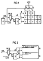
- Figure 1 shows a first embodiment of the invention integrated memory which is a DRAM and first Memory areas 1 and second memory areas 2 in the form of Has memory blocks.
- the first memory areas 1 serve in both a first and a second operating mode of memory storing via a data bus DB user data transmitted by a processor 4.
- the second Memory areas 2 are only used in the first operating mode Storage of those stored in the first storage areas 1 Error correction data assigned to user data.
- the second memory areas 2 are used not storing error correction data, but instead deactivated.
- By opening with a supply potential VCC of the switches S connected to the memory become the second Memory areas 2 in the second operating mode of the supply potential VCC disconnected so that their power consumption subsequently is zero.
- the second operating mode So it is an energy saving mode of this embodiment the invention.
- the energy saving mode no separation of the second memory area from the supply voltage respectively. Instead, with a DRAM for example, refreshing the memory cell contents (refresh) be prevented in the second operating mode. Also this reduces electricity consumption.
- Each of the memory areas 1, 2 has a plurality of memory cells for storing one bit each of the user or error correction data on.
- the memory cells of the memory are matrix-shaped arranged and are not via a in Figure 1 row or column decoding shown, as in conventional Save as usual, addressed.
- the memory in FIG. 1 also has an error correction unit 3 to generate the in the first mode in the second memory areas 2 error correction data to be stored and to evaluate this error correction data at Reading the corresponding user data from the first memory areas 1 on.
- the Error correction unit 3 via a multiplexer MUX on the User data D lying on the data bus DB generates associated error correction data E using a suitable error correction code (such as the Hamming Code) and writes this error correction data E in one of the second memory areas 2 and the associated useful data D in one of the first memory areas 1.
- a suitable error correction code such as the Hamming Code
- the second memory areas are in the second operating mode 2 deactivated and the user data D are sent directly from the data bus DB into one of the first memory areas via the MUX multiplexer 1 written, bypassing the error correction unit 3 becomes. It is also used in the second mode Reading out this user data from the first memory areas 1 bypassed.
- the error correction unit 3 is therefore only in the activated in the first operating mode and in the second operating mode deactivated.
- the useful data D via the data bus DB between the processor 4 and the multiplexer Transfer MUX.
- the processor 4 can either Part of the same integrated circuit as that already explained components or can be on a separate one integrated circuit.
- the processor 4 is with the multiplexer MUX and the switches S over a control line CTR connected.
- the processor controls this 4, in which operating mode the memory is. If the control line CTR has a high potential, there is the memory in the first mode, which are switches S. closed and the multiplexer MUX transmits user data D via the error correction unit 3 from and to the first memory areas 1 while the error correction unit the error correction data E from and to the second memory areas 2 transmits.
- the control line CTR a low potential
- the switches S are open and the multiplexer MUX transmits the user data D from and to the first memory areas 1 bypassing the error correction unit 3.
- the latter transmits in the second mode no error correction data E from and to the second memory areas.
- the processor 4 initially stores the memory in the second mode operates with the low power consumption and that he a memory test of the first memory areas at regular intervals 1 carries out.
- the memory test is carried out by Registration of test data and subsequent readout in the first memory areas 1, the read test data be compared with the registered ones.
- the processor If there is a memory error, it moves the memory via the control line CTR from the second to the first operating mode, whereby the second memory areas 2 and Error correction function can be activated.
- the processor 4 has the function of a test unit.
- the control line CTR can for this purpose Memory e.g. also bypassing the processor 4 become.
- the desired operating mode can be selected via the control line then be set externally.
- Figure 2 shows a second embodiment of the invention integrated memory that is different from the embodiment in Figure 1 differs in that the first 1 and second 2 memory areas no longer spatially apart separated but nested within one another Memory blocks B are arranged. That is, in the first Operating mode are those in the first memory areas 1 too storing user data directly to the error correction data assigned to them adjacent in the second memory areas 2.
- the data bus DB has one Width of 40 bits, of which in the first mode but only 32 bits can be used.
- Each of the first memory areas 1 can hold a data word of user data with 32 bits.
- Each of the second memory areas 2 can contain 8 bits of error correction data take up. For storing 32 bit user data become 40 bit storage space in the first operating mode needed.
- the second memory areas 2 used to store user data. It can then data words with a width of 40 bits via the data bus DB written into the memory and read from it become.
- the data bus DB and the internal data buses point therefore 40 lines on, of which in the first mode only 32 are used.
- first and second memory areas 1, 2 can be provided in a nested arrangement of the first and second memory areas 1, 2 (corresponding to FIG. 2) to likewise deactivate the second memory areas 2, as has been explained with reference to FIG. 1.
- a spatially separate arrangement of the first and second memory areas instead of the energy-saving deactivation of the second Memory areas 2 in the second operating mode for storage to use user data, as is shown in FIG. 2 has been explained. Since the first shown in Figure 1 and second memory areas each memory blocks of the same Representing storage capacity would result in the first ten Storage areas 1 and three second storage areas 2 one Increase in the storage capacity available for user data in the second mode by 30% compared to the first Operating mode.
Landscapes
- Engineering & Computer Science (AREA)
- Theoretical Computer Science (AREA)
- Quality & Reliability (AREA)
- Physics & Mathematics (AREA)
- General Engineering & Computer Science (AREA)
- General Physics & Mathematics (AREA)
- Techniques For Improving Reliability Of Storages (AREA)
- Detection And Correction Of Errors (AREA)
Abstract
Description
- Figur 1
- ein erstes Ausführungsbeispiel des integrierten Speichers mit einer Energiesparbetriebsart und
- Figur 2
- ein zweites Ausführungsbeispiel, bei dem die Speicherkapazität des Speichers in zwei Betriebsarten jeweils unterschiedlich ist.
Claims (7)
- Integrierter Speichermit einer ersten und einer zweiten Betriebsart,mit wenigstens einem ersten Speicherbereich (1), der in beiden Betriebsarten zum Speichern von Nutzdaten dient,mit wenigstens einem zweiten Speicherbereich (2), der in der ersten, aber nicht in der zweiten Betriebsart zum Speichern von Fehlerkorrekturdaten für im ersten Speicherbereich zu speichernde Nutzdaten dient,und mit einer Fehlerkorrektureinheit (3) zur Erzeugung und Auswertung der im zweiten Speicherbereich (2) zu speichernden Fehlerkorrekturdaten, die in der ersten, aber nicht in der zweiten Betriebsart aktiviert ist.
- Speicher nach Anspruch 1,
dessen zweite Betriebsart eine Energiesparbetriebsart ist, in der der zweite Speicherbereich (2) deaktiviert ist. - Speicher nach Anspruch 1,
dessen zweiter Speicherbereich (2) in der zweiten Betriebsart zum Speichern von Nutzdaten dient. - Speicher nach Anspruch 1,
dessen erster (1) und zweiter (2) Speicherbereich räumlich voneinander getrennt sind. - Speicher nach Anspruch 1,
dessen erster (1) und zweiter (2) Speicherbereich ineinander verschachtelt angeordnet sind. - Speicher nach einem der Ansprüche 1 bis 5,
mit einer Prüfeinheit (4) zum Prüfen des ersten Speicherbereiches (1) auf Speicherfehler und zur Festlegung der Betriebsart des Speichers in Abhängigkeit des Prüfergebnisses. - Speicher nach einem der Ansprüche 1 bis 5,
der einen Anschluß zum Anlegen eines Steuersignals (CTR) hat, in dessen Abhängigkeit ein Wechsel zwischen den Betriebsarten erfolgt.
Applications Claiming Priority (2)
| Application Number | Priority Date | Filing Date | Title |
|---|---|---|---|
| DE19804035 | 1998-02-02 | ||
| DE19804035A DE19804035A1 (de) | 1998-02-02 | 1998-02-02 | Integrierter Speicher |
Publications (3)
| Publication Number | Publication Date |
|---|---|
| EP0933708A2 true EP0933708A2 (de) | 1999-08-04 |
| EP0933708A3 EP0933708A3 (de) | 1999-12-15 |
| EP0933708B1 EP0933708B1 (de) | 2003-08-20 |
Family
ID=7856404
Family Applications (1)
| Application Number | Title | Priority Date | Filing Date |
|---|---|---|---|
| EP99101470A Expired - Lifetime EP0933708B1 (de) | 1998-02-02 | 1999-01-27 | Integrierter Speicher mit Fehlerkorrekturdaten in einer Betriebsart |
Country Status (4)
| Country | Link |
|---|---|
| US (1) | US6216248B1 (de) |
| EP (1) | EP0933708B1 (de) |
| DE (2) | DE19804035A1 (de) |
| TW (1) | TW508581B (de) |
Cited By (1)
| Publication number | Priority date | Publication date | Assignee | Title |
|---|---|---|---|---|
| EP1875477A4 (de) * | 2005-03-24 | 2008-12-17 | Freescale Semiconductor Inc | Speicher mit teil zur verwendung als datenspeicher oder fehlerkorrekturcode (ecc)-speicher |
Families Citing this family (13)
| Publication number | Priority date | Publication date | Assignee | Title |
|---|---|---|---|---|
| US7111224B1 (en) * | 2001-02-28 | 2006-09-19 | Xilinx, Inc. | FPGA configuration memory with built-in error correction mechanism |
| US6769050B1 (en) * | 2001-09-10 | 2004-07-27 | Rambus Inc. | Techniques for increasing bandwidth in port-per-module memory systems having mismatched memory modules |
| US6785782B1 (en) * | 2001-09-10 | 2004-08-31 | Rambus Inc. | Techniques for increasing bandwidth in port-per-module memory systems having mismatched memory modules |
| US6636935B1 (en) * | 2001-09-10 | 2003-10-21 | Rambus Inc. | Techniques for increasing bandwidth in port-per-module memory systems having mismatched memory modules |
| DE10145727B4 (de) * | 2001-09-17 | 2013-07-11 | Qimonda Ag | Verfahren und Vorrichtung zum Verringern des Stromverbrauchs einer elektronischen Schaltung |
| US6904540B2 (en) | 2001-10-29 | 2005-06-07 | Hewlett-Packard Development Company, L.P. | Targeted data protection |
| US20080052598A1 (en) * | 2006-08-09 | 2008-02-28 | Aksamit Slavek P | Memory multi-bit error correction and hot replace without mirroring |
| US9373377B2 (en) | 2011-11-15 | 2016-06-21 | Micron Technology, Inc. | Apparatuses, integrated circuits, and methods for testmode security systems |
| KR20160017922A (ko) * | 2014-08-07 | 2016-02-17 | 에스케이하이닉스 주식회사 | 반도체 메모리 장치 |
| JP6527054B2 (ja) * | 2015-08-28 | 2019-06-05 | 東芝メモリ株式会社 | メモリシステム |
| KR20170035103A (ko) * | 2015-09-22 | 2017-03-30 | 삼성전자주식회사 | 반도체 메모리 장치 및 이를 포함하는 메모리 시스템 |
| GB2578420B (en) * | 2018-08-08 | 2023-03-29 | Trw Ltd | A sensing apparatus |
| US11340979B2 (en) * | 2019-12-27 | 2022-05-24 | Seagate Technology Llc | Mitigation of solid state memory read failures with a testing procedure |
Family Cites Families (6)
| Publication number | Priority date | Publication date | Assignee | Title |
|---|---|---|---|---|
| US4319356A (en) * | 1979-12-19 | 1982-03-09 | Ncr Corporation | Self-correcting memory system |
| US4528666A (en) * | 1983-01-03 | 1985-07-09 | Texas Instruments Incorporated | Memory system with built in parity |
| JPS61134988A (ja) * | 1984-12-04 | 1986-06-23 | Toshiba Corp | 半導体メモリにおける誤り検出訂正機能制御系 |
| US5493574A (en) * | 1992-09-24 | 1996-02-20 | Zilog, Inc. | Power efficient RAM disk and a method of emulating a rotating memory disk |
| DE4329012A1 (de) | 1993-08-28 | 1995-03-02 | Sel Alcatel Ag | Verfahren und Vorrichtung zur Fehlerprüfung und zur Fehlerkorrektur in Speicherbausteinen |
| JPH10198608A (ja) * | 1997-01-08 | 1998-07-31 | Mitsubishi Electric Corp | メモリカード |
-
1998
- 1998-02-02 DE DE19804035A patent/DE19804035A1/de not_active Withdrawn
-
1999
- 1999-01-27 DE DE59906620T patent/DE59906620D1/de not_active Expired - Fee Related
- 1999-01-27 EP EP99101470A patent/EP0933708B1/de not_active Expired - Lifetime
- 1999-02-02 US US09/243,296 patent/US6216248B1/en not_active Expired - Lifetime
- 1999-02-02 TW TW088101493A patent/TW508581B/zh not_active IP Right Cessation
Cited By (1)
| Publication number | Priority date | Publication date | Assignee | Title |
|---|---|---|---|---|
| EP1875477A4 (de) * | 2005-03-24 | 2008-12-17 | Freescale Semiconductor Inc | Speicher mit teil zur verwendung als datenspeicher oder fehlerkorrekturcode (ecc)-speicher |
Also Published As
| Publication number | Publication date |
|---|---|
| DE19804035A1 (de) | 1999-08-05 |
| EP0933708B1 (de) | 2003-08-20 |
| DE59906620D1 (de) | 2003-09-25 |
| US6216248B1 (en) | 2001-04-10 |
| EP0933708A3 (de) | 1999-12-15 |
| TW508581B (en) | 2002-11-01 |
Similar Documents
| Publication | Publication Date | Title |
|---|---|---|
| DE102008028327B4 (de) | Speicherauffrischsystem und -Verfahren | |
| EP0933708B1 (de) | Integrierter Speicher mit Fehlerkorrekturdaten in einer Betriebsart | |
| DE3834759C2 (de) | ||
| DE4328605C2 (de) | Halbleiterspeichereinrichtung | |
| EP0527866B1 (de) | Integrierter halbleiterspeicher mit paralleltestmöglichkeit und redundanzverfahren | |
| DE112004001704B4 (de) | Verfahren zum Auffrischen eines Speichers und integrierter Schaltkreis, der einen auffrischbaren Speicher enthält | |
| DE69121801T2 (de) | Halbleiterspeicheranordnung | |
| DE3906497A1 (de) | Selbstkonfigurierendes speichersystem | |
| DE3639169A1 (de) | Halbleiterspeichervorrichtung | |
| DE2529152A1 (de) | Verfahren und anordnung zur feststellung von fehlern in halbleiter- informationsspeichern | |
| EP1113362A2 (de) | Integrierter Halbleiterspeicher mit einer Speichereinheit zum Speichern von Adressen fehlerhafter Speicherzellen | |
| DE10206689A1 (de) | Integrierter Speicher und Verfahren zum Betrieb eines integrierten Speichers | |
| EP0991079A2 (de) | Integrierter Speicher | |
| EP0990236B1 (de) | Anordnung mit speicherzellen und verfahren zur funktionsüberprüfung von speicherzellen | |
| DE69016849T2 (de) | Halbleiterspeichergerät mit Adressenunterscheidungsschaltung zur Unterscheidung einer adressenzugewiesenen Defektspeicherzelle, ersetzt mit Redundanzspeicherzelle. | |
| DE19924288B4 (de) | Integrierter Speicher | |
| WO2009062655A1 (de) | Verfahren zum prüfen eines arbeitsspeichers | |
| DE69629430T2 (de) | Austausch-Halbleiterfestwertspeicher | |
| EP1163675B1 (de) | Integrierter speicher mit speicherzellen und referenzzellen sowie betriebsverfahren für einen solchen speicher | |
| EP1163678B1 (de) | Integrierter speicher mit speicherzellen, die je einen ferroelektrischen speichertransistor aufweisen | |
| EP1163679B1 (de) | Betriebsverfahren für einen integrierten speicher mit beschreibbaren speicherzellen und entsprechender integrierter speicher | |
| WO1999014674A1 (de) | Dynamischer speicher mit zwei betriebsarten | |
| DE19903198C1 (de) | Integrierter Speicher und entsprechendes Betriebsverfahren | |
| EP0505603B1 (de) | Verfahren zum Testen eines Datenspeichers und zugehörigen Schutzspeichers und Anordnung zur Durchführung des Verfahrens | |
| DE19808347B4 (de) | Integrierter Speicher |
Legal Events
| Date | Code | Title | Description |
|---|---|---|---|
| PUAI | Public reference made under article 153(3) epc to a published international application that has entered the european phase |
Free format text: ORIGINAL CODE: 0009012 |
|
| AK | Designated contracting states |
Kind code of ref document: A2 Designated state(s): AT BE CH CY DE DK ES FI FR GB GR IE IT LI LU MC NL PT SE Kind code of ref document: A2 Designated state(s): DE FR GB IE IT |
|
| AX | Request for extension of the european patent |
Free format text: AL;LT;LV;MK;RO;SI |
|
| PUAL | Search report despatched |
Free format text: ORIGINAL CODE: 0009013 |
|
| AK | Designated contracting states |
Kind code of ref document: A3 Designated state(s): AT BE CH CY DE DK ES FI FR GB GR IE IT LI LU MC NL PT SE |
|
| AX | Request for extension of the european patent |
Free format text: AL;LT;LV;MK;RO;SI |
|
| 17P | Request for examination filed |
Effective date: 20000404 |
|
| AKX | Designation fees paid |
Free format text: DE FR GB IE IT |
|
| RAP1 | Party data changed (applicant data changed or rights of an application transferred) |
Owner name: INFINEON TECHNOLOGIES AG |
|
| 17Q | First examination report despatched |
Effective date: 20020403 |
|
| GRAH | Despatch of communication of intention to grant a patent |
Free format text: ORIGINAL CODE: EPIDOS IGRA |
|
| RIN1 | Information on inventor provided before grant (corrected) |
Inventor name: RICHTER, DETLEV Inventor name: MCCONNEL, RODERICK, DR. |
|
| GRAH | Despatch of communication of intention to grant a patent |
Free format text: ORIGINAL CODE: EPIDOS IGRA |
|
| GRAA | (expected) grant |
Free format text: ORIGINAL CODE: 0009210 |
|
| AK | Designated contracting states |
Designated state(s): DE FR GB IE IT |
|
| PG25 | Lapsed in a contracting state [announced via postgrant information from national office to epo] |
Ref country code: IT Free format text: LAPSE BECAUSE OF FAILURE TO SUBMIT A TRANSLATION OF THE DESCRIPTION OR TO PAY THE FEE WITHIN THE PRESCRIBED TIME-LIMIT;WARNING: LAPSES OF ITALIAN PATENTS WITH EFFECTIVE DATE BEFORE 2007 MAY HAVE OCCURRED AT ANY TIME BEFORE 2007. THE CORRECT EFFECTIVE DATE MAY BE DIFFERENT FROM THE ONE RECORDED. Effective date: 20030820 Ref country code: FR Free format text: LAPSE BECAUSE OF FAILURE TO SUBMIT A TRANSLATION OF THE DESCRIPTION OR TO PAY THE FEE WITHIN THE PRESCRIBED TIME-LIMIT Effective date: 20030820 |
|
| REG | Reference to a national code |
Ref country code: GB Ref legal event code: FG4D Free format text: NOT ENGLISH |
|
| REG | Reference to a national code |
Ref country code: IE Ref legal event code: FG4D Free format text: GERMAN |
|
| REF | Corresponds to: |
Ref document number: 59906620 Country of ref document: DE Date of ref document: 20030925 Kind code of ref document: P |
|
| GBT | Gb: translation of ep patent filed (gb section 77(6)(a)/1977) |
Effective date: 20031119 |
|
| PLBE | No opposition filed within time limit |
Free format text: ORIGINAL CODE: 0009261 |
|
| STAA | Information on the status of an ep patent application or granted ep patent |
Free format text: STATUS: NO OPPOSITION FILED WITHIN TIME LIMIT |
|
| 26N | No opposition filed |
Effective date: 20040524 |
|
| EN | Fr: translation not filed | ||
| PGFP | Annual fee paid to national office [announced via postgrant information from national office to epo] |
Ref country code: GB Payment date: 20070119 Year of fee payment: 9 |
|
| PGFP | Annual fee paid to national office [announced via postgrant information from national office to epo] |
Ref country code: IE Payment date: 20080122 Year of fee payment: 10 |
|
| PGFP | Annual fee paid to national office [announced via postgrant information from national office to epo] |
Ref country code: DE Payment date: 20080315 Year of fee payment: 10 |
|
| GBPC | Gb: european patent ceased through non-payment of renewal fee |
Effective date: 20080127 |
|
| PG25 | Lapsed in a contracting state [announced via postgrant information from national office to epo] |
Ref country code: GB Free format text: LAPSE BECAUSE OF NON-PAYMENT OF DUE FEES Effective date: 20080127 |
|
| REG | Reference to a national code |
Ref country code: IE Ref legal event code: MM4A |
|
| PG25 | Lapsed in a contracting state [announced via postgrant information from national office to epo] |
Ref country code: DE Free format text: LAPSE BECAUSE OF NON-PAYMENT OF DUE FEES Effective date: 20090801 |
|
| PG25 | Lapsed in a contracting state [announced via postgrant information from national office to epo] |
Ref country code: IE Free format text: LAPSE BECAUSE OF NON-PAYMENT OF DUE FEES Effective date: 20090127 |