EP0933613A2 - Verfahren und Vorrichtung zur Abstandsmessung - Google Patents
Verfahren und Vorrichtung zur Abstandsmessung Download PDFInfo
- Publication number
- EP0933613A2 EP0933613A2 EP99300397A EP99300397A EP0933613A2 EP 0933613 A2 EP0933613 A2 EP 0933613A2 EP 99300397 A EP99300397 A EP 99300397A EP 99300397 A EP99300397 A EP 99300397A EP 0933613 A2 EP0933613 A2 EP 0933613A2
- Authority
- EP
- European Patent Office
- Prior art keywords
- photoelectric conversion
- conversion elements
- transfer unit
- charges
- sensor apparatus
- Prior art date
- Legal status (The legal status is an assumption and is not a legal conclusion. Google has not performed a legal analysis and makes no representation as to the accuracy of the status listed.)
- Granted
Links
- 238000000034 method Methods 0.000 title claims description 18
- 238000009825 accumulation Methods 0.000 claims abstract description 81
- 238000006243 chemical reaction Methods 0.000 claims abstract description 43
- 238000010586 diagram Methods 0.000 description 6
- 230000010354 integration Effects 0.000 description 6
- 229920006395 saturated elastomer Polymers 0.000 description 4
- 230000000694 effects Effects 0.000 description 3
- 238000003491 array Methods 0.000 description 2
- 230000004044 response Effects 0.000 description 2
- 230000003247 decreasing effect Effects 0.000 description 1
- 238000007599 discharging Methods 0.000 description 1
- 230000001771 impaired effect Effects 0.000 description 1
- 230000000977 initiatory effect Effects 0.000 description 1
- 230000007246 mechanism Effects 0.000 description 1
- 238000012986 modification Methods 0.000 description 1
- 230000004048 modification Effects 0.000 description 1
- 230000008569 process Effects 0.000 description 1
Images



Classifications
-
- G—PHYSICS
- G01—MEASURING; TESTING
- G01C—MEASURING DISTANCES, LEVELS OR BEARINGS; SURVEYING; NAVIGATION; GYROSCOPIC INSTRUMENTS; PHOTOGRAMMETRY OR VIDEOGRAMMETRY
- G01C3/00—Measuring distances in line of sight; Optical rangefinders
- G01C3/02—Details
- G01C3/06—Use of electric means to obtain final indication
- G01C3/08—Use of electric radiation detectors
- G01C3/085—Use of electric radiation detectors with electronic parallax measurement
Definitions
- the present invention relates to a sensor apparatus applied to a distance measuring apparatus and a method for controlling the sensor apparatus and, more specifically, a sensor apparatus using a ring-shaped charge transfer device, applied to an automatic focusing mechanism of a camera, and a method for controlling the sensor apparatus.
- a distance measuring device which circulates accumulated charges, obtained by performing photoelectric conversion of light reflected by an object to be measured, using a ring-shaped charge transfer device, such as CCD, to integrate the light and measures the distance to the object on the basis of voltages of the integrated charges has been proposed by the Japanese Patent Publication No. 5-22843. Further, a modified distance measuring apparatus, which is briefly shown in Fig. 5, has been proposed by the Japanese Patent Application Laid-Open No. 8-233571.
- a light-emitting device 1 turns on and off at predetermined period.
- Light emitted by the light-emitting device 1 projects on an object (not shown) via a projection lens 2. From the object, light due to the light emitted by the light-emitting device 1 when it is on and external light, and light due to external light when the light-emitting device 1 is off is alternately received.
- the reflected light incidents on a sensor array 55 composed of sensor elements, i.e., photoelectric conversion elements, S1 to S4 of a sensor apparatus 54 via a light-receiving lens 3.
- Charges generated by the sensor elements S1 to S4 while the light-emitting device 1 is on are transferred to accumulation units ST2 via an electronic shutter ICG and sorting units ST01 to ST04. Similarly, charges generated by the sensor elements S1 to S4 while the light-emitting device 1 is off are transferred to accumulation units ST1 via the electronic shutter ICG and the sorting units ST01 to ST04.
- an initialization unit CCLR performs initialization before initiating integration of charges.
- the sorting units ST01 to ST04 are not operated so that no charge is transferred to the accumulation units ST1 and ST2.
- the electronic shutter ICG is for controlling an amount of charge to be accumulated when a charge converted from light is very large.
- the electronic shutter ICG also has a function of draining charges generated by the sensor elements S1 to S4 during the initialization of pixels C1 to C8 of a ring-shaped transfer unit 7, which will be explained later.
- a skim unit 8 composed of elements SK1 to SK3 skims a predetermined amount of charges which are unnecessary if a pair of charge amounts, obtained when the light-emitting device 1 is on and off, are large, via a clear unit SCLR, thereby preventing the pixels C1 to C8 of the ring-shaped transfer unit 7 from being saturated. Note, since charges are accumulated in the pairs of accumulation units ST1 and ST2, corresponding to the respective sensor elements S1 to S4, by obtaining a difference between the charges accumulated in each pair of the accumulation units ST1 and ST2, a signal component only due to light emitted by the light-emitting device 1 is obtained.
- a distance measuring operation in a so-called active mode performed by emitting light is explained above.
- a known distance measuring operation is performed in a passive mode.
- the above explanation, with reference to Fig. 5, is about a light beam t2 emitted from the center of the light-emitting device 1, and reflected light r2 due to the light beam t2 is received by the sensor elements S1 to S4 of the sensor array 55.
- light beams t1, t2 and t3 shown in Fig. 5 are projected onto an object or objects in order to measure distances to a plurality of points in a wide angle of view, reflected light r1 and r3 enter the lens 3 at large incident angles, and the length of the sensor array 55 may be too short to receive the reflected light r1 and r3.
- the number of sensor elements may be increased to, e.g., twice as many as the number of the sensor elements S1 to S4; however, as the number of the sensor elements increases, the numbers of the sorting units, accumulation units, pixels of the charge transfer unit 56, and pixels of the ring-shaped transfer unit 7 must be increased, which makes the configuration complicated. Further, since one circulation of charges in the ring-shaped transfer unit 7 should synchronize with one on/off operation of the light-emitting device 1, the charging period is lengthened as the number of pixels of the ring-shaped transfer unit 7 is increased, and it takes a long time to complete one distance measuring operation. In addition, since the amount of charge which can be discharged in one circulation of the ring-shaped transfer unit 7 by the skim unit 8 is fixed, the ability of removing charges due to external light deteriorates, thus the precision of a distance measuring operation is impaired.
- an apparatus in which the number of pixels of the sensor array is increased for performing a multi-point distance measuring operation while maintaining the number of pixels of a ring-shaped transfer unit as that in the apparatuses as those shown in Fig. 5 is disclosed in the Japanese Patent Application Laid-Open No. 8-320223.
- the apparatus however, more transfer pixels of a linear transfer unit for transferring charges are necessary in addition to the transfer pixels A1 to A8, thus, the size of the chip becomes large.
- the present invention has been made in consideration of the above situation, and has as its object of the present invention to make it possible to perform a multi-point distance measuring operation without increasing the number of pixels of the ring-shaped transfer unit, decreasing the driving frequency, and increasing the size of the chip. It is another object of the present invention to shorten the time to perform a multi-point distance measuring operation.
- a sensor apparatus comprising: a sensor array having a plurality of photoelectric conversion elements; a first transfer unit, having a plurality of transfer sections, for transferring charges generated by the plurality of photoelectric conversion elements; a second transfer unit, having a plurality of transfer sections, for integrating charges transferred by the first transfer unit; and a selection unit for selecting photoelectric conversion elements out of the plurality of photoelectric conversion elements and transferring charges generated by the selected photoelectric conversion elements to the first transfer unit, wherein a number of the transfer sections of the first transfer unit is greater than a number of the transfer sections of the second transfer unit.
- the foregoing object is also attained by providing a method of controlling a sensor apparatus having a sensor array having a plurality of photoelectric conversion elements, a first transfer unit, having a plurality of transfer sections, for transferring charges generated by the plurality of photoelectric conversion elements, and a second transfer unit, having a plurality of transfer sections which are fewer than the transfer sections of the first transfer unit, for integrating charges transferred by the first transfer unit, the method comprising: a step of grouping the plurality of photoelectric conversion elements into a plurality of groups; a step of selecting photoelectric conversion elements which belong to a predetermined group; and a step of transferring charges generated by the selected photoelectric conversion elements to the first transfer unit.
- Fig. 1 is a diagram illustrating a brief configuration of a sensor apparatus according to the first embodiment.
- Fig. 1 the same units and elements as those in Fig. 5 are referred to by the same reference numerals.
- a sensor array 5 of a sensor apparatus 14 comprises eight sensor elements S1 to S8. Further, a sorting unit ST01 is provided for each of the sensor elements S1 and S2, a sorting unit ST02 is provided for each of the sensor elements S3 and S4, a sorting unit ST03 is provided for each of the sensor elements S5 and S6, and a sorting unit ST04 is provided for each of the sensor elements S7 and S8.
- accumulation units ST1 and ST2 are provided, and for the respective accumulation units ST1 and ST2, transfer pixels A1 to A16 of the charge transfer unit 6 are provided. Between the sixteen accumulation units ST1 and ST2 and the sixteen transfer pixels A1 to A16, sixteen shift gates are provided.
- the electronic shutter ICG is for controlling the amount of charge to be accumulated when the charge converted from light is very large.
- the electronic shutter ICG also has a function of draining charges generated by the sensor elements S1 to S8 during the initialization, performed in advance of integration, of the pixels C1 to C8 of the ring-shaped transfer unit 7.
- the sorting units ST01 to ST04 do not operate during the initialization so that no charge is transferred to the accumulation units ST1 and ST2.
- the light-emitting device 1, the projection lens 2, and the light-receiving lens 3, shown in Fig. 5, are not shown in Fig. 1; however, these elements are also provided similarly to Fig. 5.
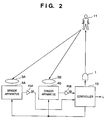
- Fig. 2 shows a brief configuration of the distance measuring apparatus using the two sensor apparatuses 14 as shown in Fig. 1.
- first and second sensor apparatuses 4A and 4B are arranged at a predetermined interval.
- a controller 10 controls the sensor apparatuses 4A and 4B, and, when performing a distance measuring operation in the active mode, on/off of the light-emitting device 1.
- Light emitted from the light-emitting device 1 is projected on an object 11.
- Reflected light from the object 11 is received by the sensor apparatuses 4A and 4B via light-receiving lenses 3A and 3B, and charges obtained as a result of photoelectric conversion are transferred and integrated, then outputted as signals SA and SB via amplifiers FGA and FGB.
- the controller 10 performs a correlation operation on the signals SA and SB to obtain a distance L to the object 11.
- the sensor elements S1 to S8 of the sensor array 5 are grouped into four groups each having adjoining two sensor elements, and two groups out of the four groups are sequentially selected by the sorting units ST01 to ST04, as shown in the following table 1, in each distance measuring operation. More specifically, for receiving the light r3, shown in Fig. 5, the sensor elements S1 to S4 which are in the left portion of the sensor array 5 are selected, and for receiving the light r2, the sensor elements S3 to S6 which are in the central portion of the sensor array 5 are selected, and for receiving the light r1, the sensor elements S5 to S8 which are in the right portion of the sensor array 5 are selected.
- the charges, transferred to the pairs of the accumulation units ST1 and ST2, are transferred to the transfer pixels A1 to A16.
- the transferred charges are shifted toward the pixels C1 to C8 of the ring-shaped transfer unit 7 via the transfer pixels B1 to B4.
- the light emission is performed in synchronization with the transference of the charges, and the charges obtained from the sensor elements S1 to S8 during each ON/OFF operation of the light-emitting device 1 are respectively integrated in the pixels C1 to C8.
- not all the charges generated during each ON/OFF operation of the light-emitting device 1 are transferred to the transfer pixels A1 to A16, as described above. More specifically, charges generated by four sensor elements are transferred to eight pixels out of the sixteen pixels A1 to A16, and shifted toward the pixels C1 to C8, and no charge is transferred to the rest of the pixels A1 to A16. Therefore, charges transferred to the eight pixels out of the pixels A1 to A16 are shifted to the pixels C1 to C8 and integrated there without being mixed with charges of different sensor elements.
- the skim unit 8 removes a predetermined amount of charge in response to a signal SCLR when the amounts of each pair of charges obtained while the light-emitting device is on and while it is off are large, to prevent the pixels C1 to C8 from being saturated. Furthermore, the difference between the changes, outputted from the accumulation units ST1 and ST2, and integrated in the pixels C1 to C8, are obtained, thereby obtaining a signal component corresponding to a charge due to light emitted by the light-emission device 1(???).
- the eight sorting units ST01 to ST04 which operate in four different patterns by two units are provided for the sensor elements S1 to S8, and the two accumulation units ST1 and ST2 are provided for each sensor element.
- the present invention is not limited to this, and the number of elements and units may be increased.
- the sensor array in more groups greater than two, and transferring charges obtained from two or more adjoining groups, it is possible to freely cope with a multi-point distance measuring operation for measuring distances to a plurality of positions (objects) of an image formed on the sensor arrays or the distance to an object whose image forming positions on the sensor arrays changes in correspondence with the distance to the object.
- two charge accumulation units provided for each photoelectric conversion element of a sensor array make it easier to separately integrate charges, generated during an on period and an off period of the light-emitting device, in synchronization with the on/off operation.
- transference of charges from the sensor elements S1 to S8 is controlled differently in the active mode and in the passive mode.
- Fig. 3 is a diagram illustrating a brief configuration of a sensor apparatus according to the second embodiment.
- Fig. 3 the same units and elements as those in Fig. 5 are referred to by the same reference numerals.
- the sensor array 5 of a sensor apparatus 24 comprises the eight sensor elements S1 to S8. Further, the sorting unit ST01 is provided for each of the sensor elements S1 and S2, the sorting unit ST02 is provided for each of the sensor elements S3 and S4, the sorting unit ST03 is provided for each of the sensor elements S5 and S6, and the sorting unit ST04 is provided for each of the sensor elements S7 and S8.
- accumulation units ST1' and ST2 are provided, and for each of the sorting units ST03 and ST04, accumulation units ST1 and ST2' are provided. Further, for the respective accumulation units ST1', ST2, ST1, and ST2', transfer pixels A1 to A16 of the charge transfer unit 6, having four transfer pixels B1 to B4, are provided. Between the sixteen accumulation units ST1, ST1', ST2 and ST2' and the sixteen transfer pixels A1 to A16, sixteen shift gates are provided.
- the electronic shutter ICG is for controlling the amount of charge to be accumulated when a charge converted from light is very large.
- the electronic shutter ICG also has a function of draining charges generated by the sensor elements S1 to S8 during the initialization, performed in advance of integration, of the pixels C1 to C8 of the ring-shaped transfer unit 7.
- the sorting units ST01 to ST04 do not operate during the initialization so that no charge is transferred to the accumulation units ST1, ST1', ST2 and ST2'.
- the light-emitting device 1, the projection lens 2, and the light-receiving lens 3, shown in Fig. 5, are not shown in Fig. 3; however, these elements are also provided similarly to Fig. 5.
- the sensor elements S1 to S8 of the sensor array 5 are grouped into four groups each having adjoining two sensor elements, and two groups out of the four groups are sequentially selected by the sorting units ST01 to ST04, as shown in the following table 2, in each distance measuring operation, in the active mode. More specifically, for receiving the light r3 shown in Fig. 5, the sensor elements S1 to S4 which are in the left portion of the sensor array 5 are selected, and for receiving the light r2, the sensor elements S3 to S6 which are in the central portion of the sensor array 5 are selected, and for receiving the light r1, the sensor elements S5 to S8 which are in the right portion of the sensor array 5 are selected.
- the sorting units ST03 and ST04 are selected in the active mode, for instance, since charges are circulated in the ring shaped transfer unit, at a given time the charge of the accumulation unit ST1 of the sensor element S8 is transferred to the pixel C8 of the ring-shaped transfer unit 7; the charge of the accumulation unit ST2' of the sensor element S8, to the pixel C7; the charge of the accumulation unit ST1 of the sensor element S7, to the pixel C6; the charge of the accumulation unit ST2' of the sensor element S7, to the pixel C5; the charge of the accumulation unit ST1 of the sensor element S6, to the pixel C4; the charge of the accumulation unit ST2' of the sensor element S6, to the pixel C3; the charge of the accumulation unit ST1 of the sensor element S5, to the pixel C2; and the charge of the accumulation unit ST2' of the sensor element S5, to the pixel C1.
- the skim unit 8 removes a predetermined amount of charge in response to a signal SCLR when the amounts of each pair of charges obtained while the light-emitting device is on and while it is off are large, to prevent the pixels C1 to C8 from being saturated. Furthermore, the difference between the changes, outputted from the accumulation units ST1 and ST2, and integrated in the pixels C1 to C8, are obtained, thereby obtaining a signal component corresponding to the charge due to light emitted by the light-emission device 1.
- skimming operation is not performed, further, the difference between the pairs of charges is not obtained, and only the charges accumulated in the accumulation units ST1 and ST2 are transferred and integrated, as shown in the table 2.
- the accumulation units ST1' and ST2' are not operated in the passive mode, as shown in the table 2, and all the sorting units ST01 to ST04 operate.
- the charge of the accumulation unit ST1 of the sensor element S8 is transferred to the pixel C8 of the ring-shaped transfer unit 7; the charge of the accumulation unit ST1 of the sensor element S7, to the pixel C7; the charge of the accumulation unit ST1 of the sensor element S6, to the pixel C6; the charge of the accumulation unit ST1 of the sensor element S5, to the pixel C5; the charge of the accumulation unit ST2 of the sensor element S4, to the pixel C4; the charge of the accumulation unit ST1 of the sensor element S3, to the pixel C3; the charge of the accumulation unit ST2 of the sensor element S2, to the pixel C2; and the charge of the accumulation unit ST2 of the sensor element S1, to the pixel C1.
- the passive mode the number of sensor elements which can be integrated in the ring-shaped transfer unit 7 is doubled compared with the active mode. Accordingly, in the passive mode, it is possible to perform correlation operation on the basis of signals obtained in one integrating operation.
- the eight sorting units ST01 to ST04 which operate in four different patterns by two units are provided for the sensor elements S1 to S8, and the two accumulation units ST1' and ST2 or ST1 and ST2' are provided for each sensor element.
- the present invention is not limited to this, and the number of elements and units may be increased.
- charges stored in the accumulation units ST2 of the sensor elements S1 to S4 and charges stored in the accumulation units ST1 of the sensor elements S5 to S8 are integrated in the ring-shaped transfer unit 7; however, the present invention is not limited to this, and a charge stored in either one of the two accumulation units provided for each of the sensor elements S1 to S8 can be integrated. For instance, it is possible to configure the sensor apparatus so that charges stored in the accumulation units ST2 and ST1' of the sensor elements S1 to S8 are integrated.
- Fig. 4 shows a configuration of a sensor apparatus according to the third embodiment, and the same units and elements as those in Fig. 1 are referred to by the same reference numerals.
- the accumulation units ST1 and ST2, and shift gates SH1 and SH2 are provided for each of the sorting units ST01 to ST04. Charges accumulated in the accumulation units ST1 of the sensor elements S1 to S4 and the accumulation units ST2 of the sensor elements S5 to S8 are transferred via the shift gates SH1, and charges accumulated in the accumulation units ST2 of the sensor elements S1 to S4 and the accumulation units ST1 of the sensor elements S5 to S8 are transferred via the shift gates SH2.
- the following table 3 shows the control of the shift gates SH1 and SH2.
- the sorting units ST01 to ST04 are controlled in accordance with the table 2.
- the eight sorting units ST01 to ST04 which operate in four different patterns by two units are provided for the sensor elements S1 to S8, and the two accumulation units ST1 and ST2 are provided for each sensor element.
- the present invention is not limited to this, and the number of elements and units may be increased.
Landscapes
- Physics & Mathematics (AREA)
- Electromagnetism (AREA)
- Engineering & Computer Science (AREA)
- General Physics & Mathematics (AREA)
- Radar, Positioning & Navigation (AREA)
- Remote Sensing (AREA)
- Measurement Of Optical Distance (AREA)
- Solid State Image Pick-Up Elements (AREA)
- Focusing (AREA)
Applications Claiming Priority (4)
| Application Number | Priority Date | Filing Date | Title |
|---|---|---|---|
| JP10016487A JPH11211461A (ja) | 1998-01-29 | 1998-01-29 | 測距装置 |
| JP1648798 | 1998-01-29 | ||
| JP10018415A JPH11211463A (ja) | 1998-01-30 | 1998-01-30 | 測距装置 |
| JP1841598 | 1998-01-30 |
Publications (3)
| Publication Number | Publication Date |
|---|---|
| EP0933613A2 true EP0933613A2 (de) | 1999-08-04 |
| EP0933613A3 EP0933613A3 (de) | 2000-08-30 |
| EP0933613B1 EP0933613B1 (de) | 2005-04-27 |
Family
ID=26352836
Family Applications (1)
| Application Number | Title | Priority Date | Filing Date |
|---|---|---|---|
| EP99300397A Expired - Lifetime EP0933613B1 (de) | 1998-01-29 | 1999-01-20 | Verfahren und Vorrichtung zur Abstandsmessung |
Country Status (3)
| Country | Link |
|---|---|
| US (1) | US6035138A (de) |
| EP (1) | EP0933613B1 (de) |
| DE (1) | DE69924897T2 (de) |
Families Citing this family (5)
| Publication number | Priority date | Publication date | Assignee | Title |
|---|---|---|---|---|
| JP2000249906A (ja) * | 1999-02-26 | 2000-09-14 | Canon Inc | 撮像装置と測距装置 |
| JP2001141987A (ja) * | 1999-11-17 | 2001-05-25 | Olympus Optical Co Ltd | 測距装置 |
| JP2003107340A (ja) * | 2001-09-27 | 2003-04-09 | Canon Inc | 測光測距用固体撮像装置及びそれを用いた撮像装置 |
| JP2003215442A (ja) * | 2002-01-25 | 2003-07-30 | Canon Inc | 多点測距装置 |
| JP4804027B2 (ja) * | 2005-04-21 | 2011-10-26 | キヤノン株式会社 | 焦点検出用固体撮像装置 |
Family Cites Families (9)
| Publication number | Priority date | Publication date | Assignee | Title |
|---|---|---|---|---|
| US4521106A (en) * | 1982-08-18 | 1985-06-04 | Eastman Kodak Company | Image sensor and rangefinder device with background subtraction using interlaced analog shift register |
| JPS60105270A (ja) * | 1983-11-11 | 1985-06-10 | Canon Inc | 投光式距離計における光電変換装置 |
| JPH0522843A (ja) * | 1991-07-09 | 1993-01-29 | Mitsubishi Electric Corp | 地絡方向継電装置 |
| JP3471957B2 (ja) * | 1995-02-28 | 2003-12-02 | キヤノン株式会社 | 測距装置 |
| JPH08320223A (ja) * | 1995-05-26 | 1996-12-03 | Canon Inc | 測距装置 |
| US5808726A (en) * | 1995-02-28 | 1998-09-15 | Canon Kabushiki Kaisha | Distance measurement apparatus |
| US5850282A (en) * | 1995-10-11 | 1998-12-15 | Canon Kabushiki Kaisha | Distance measuring device |
| JPH09229680A (ja) * | 1996-02-20 | 1997-09-05 | Canon Inc | 測距装置 |
| US5870178A (en) * | 1996-02-20 | 1999-02-09 | Canon Kabushiki Kaisha | Distance measuring apparatus |
-
1999
- 1999-01-15 US US09/231,796 patent/US6035138A/en not_active Expired - Fee Related
- 1999-01-20 DE DE69924897T patent/DE69924897T2/de not_active Expired - Lifetime
- 1999-01-20 EP EP99300397A patent/EP0933613B1/de not_active Expired - Lifetime
Also Published As
| Publication number | Publication date |
|---|---|
| EP0933613B1 (de) | 2005-04-27 |
| EP0933613A3 (de) | 2000-08-30 |
| DE69924897T2 (de) | 2006-02-23 |
| US6035138A (en) | 2000-03-07 |
| DE69924897D1 (de) | 2005-06-02 |
Similar Documents
| Publication | Publication Date | Title |
|---|---|---|
| US6781632B1 (en) | Image pick-up apparatus capable of focus detection | |
| JP4007713B2 (ja) | 撮像装置 | |
| JPH04177211A (ja) | 合焦位置検出装置 | |
| US5784655A (en) | Focus detecting apparatus having photoelectric area sensors | |
| US5943514A (en) | Focusing system | |
| EP0730167B1 (de) | Entfernungsmessgerät | |
| JP3442426B2 (ja) | 光電変換装置 | |
| US7102675B1 (en) | Photoelectric conversion device, focus detection device, method of controlling these devices, and storage medium | |
| US5539493A (en) | Autofocus camera | |
| US6035138A (en) | Sensor apparatus applied to distance measuring apparatus, and method for controlling sensor apparatus | |
| JP2911521B2 (ja) | センサ装置 | |
| US5850282A (en) | Distance measuring device | |
| US5615399A (en) | Focus detecting apparatus having photoelectric area sensors | |
| US6160613A (en) | Charging condition control in distance measuring mechanism | |
| JP2002196227A (ja) | 測距センサ及び測距装置 | |
| JPH0588445B2 (de) | ||
| JPH11205694A (ja) | 光電変換装置及び焦点検出装置 | |
| US5842058A (en) | Accumulation time control device for photoelectric conversion element, and focus detection apparatus using the same | |
| JP4642547B2 (ja) | 焦点検出装置 | |
| JP2679700B2 (ja) | 自動焦点調節装置 | |
| US6310649B1 (en) | Image pickup apparatus in which storage control is separately carried out for each focus detection area group | |
| JP4700588B2 (ja) | 光電変換装置及び焦点検出装置 | |
| JP6803941B2 (ja) | 撮像システム、撮像装置、レンズ装置、撮像システムの制御方法 | |
| JP2005148229A (ja) | 光電変換装置および自動焦点検出装置 | |
| JPS62148910A (ja) | 焦点検出装置 |
Legal Events
| Date | Code | Title | Description |
|---|---|---|---|
| PUAI | Public reference made under article 153(3) epc to a published international application that has entered the european phase |
Free format text: ORIGINAL CODE: 0009012 |
|
| AK | Designated contracting states |
Kind code of ref document: A2 Designated state(s): DE FR GB |
|
| AX | Request for extension of the european patent |
Free format text: AL;LT;LV;MK;RO;SI |
|
| PUAL | Search report despatched |
Free format text: ORIGINAL CODE: 0009013 |
|
| AK | Designated contracting states |
Kind code of ref document: A3 Designated state(s): AT BE CH CY DE DK ES FI FR GB GR IE IT LI LU MC NL PT SE |
|
| AX | Request for extension of the european patent |
Free format text: AL;LT;LV;MK;RO;SI |
|
| 17P | Request for examination filed |
Effective date: 20010123 |
|
| AKX | Designation fees paid |
Free format text: DE FR GB |
|
| 17Q | First examination report despatched |
Effective date: 20031021 |
|
| GRAP | Despatch of communication of intention to grant a patent |
Free format text: ORIGINAL CODE: EPIDOSNIGR1 |
|
| GRAS | Grant fee paid |
Free format text: ORIGINAL CODE: EPIDOSNIGR3 |
|
| GRAA | (expected) grant |
Free format text: ORIGINAL CODE: 0009210 |
|
| AK | Designated contracting states |
Kind code of ref document: B1 Designated state(s): DE FR GB |
|
| REG | Reference to a national code |
Ref country code: GB Ref legal event code: FG4D |
|
| REF | Corresponds to: |
Ref document number: 69924897 Country of ref document: DE Date of ref document: 20050602 Kind code of ref document: P |
|
| PLBE | No opposition filed within time limit |
Free format text: ORIGINAL CODE: 0009261 |
|
| STAA | Information on the status of an ep patent application or granted ep patent |
Free format text: STATUS: NO OPPOSITION FILED WITHIN TIME LIMIT |
|
| ET | Fr: translation filed | ||
| 26N | No opposition filed |
Effective date: 20060130 |
|
| PGFP | Annual fee paid to national office [announced via postgrant information from national office to epo] |
Ref country code: FR Payment date: 20110209 Year of fee payment: 13 Ref country code: DE Payment date: 20110131 Year of fee payment: 13 |
|
| PGFP | Annual fee paid to national office [announced via postgrant information from national office to epo] |
Ref country code: GB Payment date: 20110125 Year of fee payment: 13 |
|
| GBPC | Gb: european patent ceased through non-payment of renewal fee |
Effective date: 20120120 |
|
| REG | Reference to a national code |
Ref country code: FR Ref legal event code: ST Effective date: 20120928 |
|
| PG25 | Lapsed in a contracting state [announced via postgrant information from national office to epo] |
Ref country code: DE Free format text: LAPSE BECAUSE OF NON-PAYMENT OF DUE FEES Effective date: 20120801 Ref country code: GB Free format text: LAPSE BECAUSE OF NON-PAYMENT OF DUE FEES Effective date: 20120120 |
|
| REG | Reference to a national code |
Ref country code: DE Ref legal event code: R119 Ref document number: 69924897 Country of ref document: DE Effective date: 20120801 |
|
| PG25 | Lapsed in a contracting state [announced via postgrant information from national office to epo] |
Ref country code: FR Free format text: LAPSE BECAUSE OF NON-PAYMENT OF DUE FEES Effective date: 20120131 |