EP0932053A1 - Strahlungsdetektor und verfahren zu seiner herstellung - Google Patents
Strahlungsdetektor und verfahren zu seiner herstellung Download PDFInfo
- Publication number
- EP0932053A1 EP0932053A1 EP98902185A EP98902185A EP0932053A1 EP 0932053 A1 EP0932053 A1 EP 0932053A1 EP 98902185 A EP98902185 A EP 98902185A EP 98902185 A EP98902185 A EP 98902185A EP 0932053 A1 EP0932053 A1 EP 0932053A1
- Authority
- EP
- European Patent Office
- Prior art keywords
- light
- receiving
- protective film
- moisture
- film
- Prior art date
- Legal status (The legal status is an assumption and is not a legal conclusion. Google has not performed a legal analysis and makes no representation as to the accuracy of the status listed.)
- Granted
Links
Images


Classifications
-
- G—PHYSICS
- G01—MEASURING; TESTING
- G01T—MEASUREMENT OF NUCLEAR OR X-RADIATION
- G01T1/00—Measuring X-radiation, gamma radiation, corpuscular radiation, or cosmic radiation
- G01T1/16—Measuring radiation intensity
- G01T1/20—Measuring radiation intensity with scintillation detectors
-
- G—PHYSICS
- G01—MEASURING; TESTING
- G01T—MEASUREMENT OF NUCLEAR OR X-RADIATION
- G01T1/00—Measuring X-radiation, gamma radiation, corpuscular radiation, or cosmic radiation
- G01T1/16—Measuring radiation intensity
- G01T1/20—Measuring radiation intensity with scintillation detectors
- G01T1/2018—Scintillation-photodiode combinations
- G01T1/20188—Auxiliary details, e.g. casings or cooling
- G01T1/20189—Damping or insulation against damage, e.g. caused by heat or pressure
Definitions
- the present invention relates to a radiation detection device; and, in particular, to a radiation detection device having a light-receiving portion with a large area, which is used for medical X-raying and the like.
- X-ray sensitive films have conventionally been used for medical and industrial X-raying
- radiation imaging systems using a radiation detection device are becoming pervasive due to their convenience and the storability of their photographed results.
- a radiation imaging system uses a radiation detection device having a plurality of pixels so as to acquire, as an electric signal, two-dimensional image data formed by a radiation, and processes thus obtained signal with a processing unit, so as to display it on a monitor.
- a typical radiation detection device is configured such that a scintillator is disposed on one- or two-dimensionally arranged photodetectors so as to convert the incident radiation into light, which is then detected.
- CsI a typical scintillator material
- a typical scintillator material is a hygroscopic material which dissolves by absorbing vapor (moisture) in the air.
- characteristics of the scintillator such as resolution in particular, have disadvantageously deteriorated.
- a radiation detection device having a structure for protecting the scintillator against moisture is the technique disclosed in Japanese Patent Application Laid-Open No. 5-196742.
- a water-impermeable moisture-proof barrier is formed on the upper side of the scintillator layer, thereby protecting the scintillator against moisture.
- the above-mentioned technique discloses a method of making a moisture seal layer for the moisture-proof barrier in which a silicone potting material or the like is coated on the scintillator layer in a liquid state or coated inside a window member disposed on the light-receiving surface side of the radiation detection device and then the window member is disposed on the scintillator layer before the moisture seal layer is dried, thereby fixing the moisture seal layer.
- a silicone potting material or the like is coated on the scintillator layer in a liquid state or coated inside a window member disposed on the light-receiving surface side of the radiation detection device and then the window member is disposed on the scintillator layer before the moisture seal layer is dried, thereby fixing the moisture seal layer.
- this method it is hard to uniformly form the moisture seal layer on a scintillator layer having an irregular surface form, whereby adhesion may deteriorate. This phenomenon tends to occur in radiation detection devices having a large area, in particular.
- the radiation detection device of the present invention comprises: (1) a light-receiving device array in which a plurality of light-receiving devices are one- or two-dimensionally arranged on a substrate to form a light-receiving portion, and a plurality of bonding pads electrically connected to the light-receiving devices in respective rows or columns of the light-receiving portion are disposed outside the light-receiving portion; (2) a scintillator layer, deposited on the light-receiving devices, for converting a radiation into visible light; (3) a radiation-transmittable, moisture-resistant protective film, constituted by a multilayer film made of at least two layers including an organic film and an inorganic film laminated thereon, covering at least the scintillator layer and exposing at least the bonding pad portion of the light-receiving device array; and (4) a coating resin coated on the moisture-resistant protective film along an edge acting as a boundary portion with respect to an exposed portion of the
- the incident radiation is converted into visible light by the scintillator layer.
- the resulting visible light image is detected by the one- or two-dimensionally arranged light-receiving devices, an electric signal corresponding to the incident radiation image is obtained.
- the scintillator layer has a characteristic of deteriorating by absorbing moisture. In the present invention, however, since the scintillator layer is covered with the moisture-resistant protective film, and an edge of the moisture-resistant protective film is coated with the coating resin, the scintillator layer is completely hermetically sealed so as to be isolated from the external atmosphere, thus being protected against vapor in the air. Further, the bonding pad portion for connection with an external circuit is exposed.
- the method of making a radiation detection device in accordance with the present invention comprises: (1) a step of forming a light-receiving portion by one- or two-dimensionally arranging a plurality of light-receiving devices on a substrate, and depositing a scintillator layer for converting a radiation into visible light on the light-receiving devices of a light-receiving device array in which a plurality of bonding pads electrically connected to the light-receiving devices in respective rows or columns of the light-receiving portion are disposed outside the light-receiving portion; (2) a step of forming a radiation-transmittable first organic film such as to envelope the light-receiving device array as a whole; (3) a step of laminating at least one layer of film including an inorganic film on the first organic film so as to form a radiation-transmittable, moisture-resistant protective film constituted by a multilayer film made of at least two layers; (4) a step of cutting and
- the adhesion between the scintillator layer and the organic film improves, thereby forming a uniform film.
- the uniform moisture-resistant protective film is removed from the bonding pad portion after being formed thereon, the bonding pad portion is securely exposed. Further, as the moisture-resistant protective film is coated with a resin along an edge portion acting as a boundary with respect to the exposed portion, the edge of the moisture-resistant protective film comes into close contact with the light-receiving device array surface thereunder, whereby the scintillator layer under the moisture-resistant protective film is sealed.
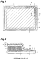
- Fig. 1 is a top plan view showing an embodiment of the present invention
- Fig. 2 is an enlarged sectional view of its outer peripheral portion taken along the line A-A.
- each light-receiving device 2 is constituted by a photodiode (PD) made of amorphous silicon or a thin-film transistor (TFT).
- PD photodiode
- TFT thin-film transistor
- a plurality of bonding pads 4 for taking out signals to an external circuit are disposed along outer peripheral sides, e.g., two adjacent sides, of the substrate 1 and are electrically connected to their corresponding plurality of light-receiving devices 2 via the signal lines 3.
- An insulating passivation film 5 is formed on the light-receiving devices 2 and signal lines 3.
- silicon nitride or silicon oxide is preferably used.
- the bonding pads 4 are exposed for connection with the external circuit.
- this substrate and the circuit portion on the substrate are referred to as a light-receiving device array 6.
- a scintillator 7 Formed on the light-receiving portion of the light-receiving device array 6 is a scintillator 7, having a columnar structure, for converting an incident radiation into visible light. Though various materials can be used for the scintillator 7, Tl-doped CsI or the like, which has a favorable emission efficiency, is preferable. Laminated on the scintillator 7 are a first organic film 8, an inorganic film 9, and a second organic film 10, each transmitting X-rays therethrough but blocking vapor, thereby forming a protective film 11.
- a poly-para-xylylene resin manufactured by Three Bond Co., Ltd.; trade name: Parylene
- poly-para-chloroxylylene manufactured by the same company; trade name: Parylene C
- the coating film made of Parylene has excellent characteristics suitable for the organic films 8, 10 in that, for example, it transmits therethrough only a very small amount of vapor and gasses, has high water repellency and chemical resistance, exhibits excellent electrical insulation even in a thin film, and is transparent to radiation and visible light.
- the details of the coating with Parylene are described in Three Bond Technical News (issued September 23, 1992), and their characteristics will be noted here.
- Parylene can be coated by chemical vapor deposition (CVD) method in which it is vapor-deposited on a support in vacuum as with the vacuum vapor deposition of metals.
- This method comprises a step of thermally decomposing p-xylene, which is a raw material, and rapidly cooling the resulting product in an organic solvent such as toluene or benzene, so as to yield di-para-xylylene which is known as dimer; a step of thermally decomposing this dimer so as to generate a stable radical para-xylylene gas; and a step of causing thus generated gas to be absorbed and polymerized on a material so as to form a poly-para-xylylene film having a molecular weight of about 500,000 by polymerization.
- CVD chemical vapor deposition
- the pressure at the time of Parylene vapor deposition is 0.1 to 0.2 torr, which is higher than the pressure in the case of metal vacuum vapor deposition, 0.001 torr.
- a monomolecular film covers the whole material to be coated, and then Parylene is further vapor-deposited thereon. Consequently, a thin film having a thickness as small as 0.2 ⁇ m can be formed with a uniform thickness in the state free of pinholes. Therefore, the coating on acute angle portions, edge portions, and narrow gaps of the order of microns, which has been impossible with liquid materials, can be effected.
- the coating can be effected at-a temperature close to room temperature, without needing heat treatment and the like at the time of coating. As a consequence, mechanical stress or thermal distortion accompanying hardening would not occur, and the coating is excellent in stability as well. Further, coating is possible with respect to almost any solid material.
- the inorganic film 9 various materials such as those transparent, opaque, or reflective to visible light can be used as long as they can transmit X-rays therethrough. Oxidized films of Si, Ti, and Cr, and metal thin films of gold, silver, aluminum, and the like can be used. In particular, a film reflective to visible light is preferably used, since it is effective in preventing fluorescence generated in the scintillator 7 from leaking out, thereby enhancing sensitivity.
- Al which is easy to shape will be explained. Though Al itself is likely to corrode in the air, the inorganic film 9 is protected against corrosion since it is held between the first organic film 8 and the second organic film 10.
- the outer periphery of the protective film 11 extends to the inside of the bonding pads 4 between the respective outer peripheries of the light receiving portion and the light-receiving device array 6, whereby the bonding pads 4 are exposed for connection with the external circuit.
- this protective film 11 is formed by the above-mentioned Parylene coating, since it is formed by CVD method, it is formed such as to cover the whole surface of the light-receiving device array 6. Therefore, in order to expose the bonding pads 4, it is necessary that the protective film 11 formed by the Parylene coating be cut inside the bonding pads 4, and the outer part of the protective film 11 be removed. In this case, the protective film 11 would be likely to peel off from the outer peripheral portion acting as the cutting portion. Therefore, the outer peripheral portion of the protective film 11 and the passivation film 5 portion of the light-receiving device array 6 at the outer periphery thereof are coated and covered with a coating resin 12.
- a resin which favorably adheres to the protective film 11 and passivation film 5 such as WORLD ROCK No. 801-SET2 (70,000 cP type) manufactured by Kyoritsu Chemical Industries Co., Ltd., which is an acrylic adhesive, for example, is preferably used.
- This resin adhesive is hardened in about 20 seconds upon UV irradiation at 100 mW/cm 2 .
- hardened coating film is soft but has a sufficient strength, is excellent in resistances to moisture, water, galvanic corrosion, and migration, favorably adheres to various materials such as glass, plastics, and the like in particular, and thus has favorable characteristics as the coating resin 12.
- CsI which forms the layer of scintillator 7 is highly hygroscopic, so that it dissolves by absorbing vapor in the air when left exposed.
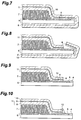
- CVD method is used for enveloping the surfaces of the whole substrate with Parylene at a thickness of 10 ⁇ m, thereby forming the first organic film 8.
- Parylene intrudes into these narrow gaps, whereby the first organic film 8 comes into close contact with the scintillator layer 7.
- the Parylene coating yields a precision thin film coating with a uniform thickness on the layer of scintillator 7 having irregularities. Since Parylene can be formed by CVD at a lower vacuum than in the case with the metal vapor deposition and at normal temperature as mentioned above, it can be processed easily.
- an Al film having a thickness of 0.15 ⁇ m is laminated on the surface of the first organic film 8 on the entrance side by vapor deposition method, thus forming the inorganic film 9.
- the surface of the whole substrate is coated with Parylene at a thickness of 10 ⁇ m as shown in Fig. 7, thereby forming the second organic film 10.
- This second organic film 10 prevents the inorganic film 9 from deteriorating due to corrosion.
- protective film 11 is cut with an excimer laser or the like along the outer periphery of the light-receiving portion at the part inside the bonding pads 4 between the light-receiving portion and the outer peripheral portion of the light-receiving device array 6 as shown in Fig. 8, and then, from thus cut portion, the unnecessary parts of the protective film 11 on the outer side thereof and the rear side of the entrance surface are removed as shown in Fig. 9, so as to expose the bonding pads 4 for connection with the external circuit. Since the passivation film 5 and the first organic film 7 disposed as the lowermost layer of the protective film 11 do not adhere well to each other, the protective film 11 will be likely to peel off if the cut outer peripheral portion is left as it is. Therefore, as shown in Fig.
- the outer peripheral portion of the protective film 11 and the part of the passivation film 5 therearound are coated and covered with the coating resin 12, which is then hardened upon UV irradiation, whereby the protective film 11 closely adheres onto the light-receiving device array 6.
- the scintillator 7 is hermetically sealed, whereby resolution can be prevented from deteriorating due to moisture absorption.
- each light-receiving device 2 an electric signal corresponding to the light quantity of the visible light is generated by photoelectric conversion and is stored for a predetermined period of time. Since the light quantity of the visible light reaching the light-receiving device 2 corresponds to the dose of the incident X-ray, the electric signal stored in each light-receiving device 2 corresponds to the dose of the incident X-ray, whereby an image signal corresponding to an X-ray image is obtained.
- the image signals stored in the light-receiving devices 2 are sequentially read out from the bonding pads 4 via the signal lines 3, transferred to the outside, and processed in a predetermined processing circuit, whereby the X-ray image can be displayed.
- the foregoing explanation relates to the protective film 11 having a configuration in which the inorganic film 9 is held between the first and second organic films 8, 10 made of Parylene, the first organic film 8 and the second organic film 10 may be made of materials different from each other. Also, when a material highly resistant to corrosion is used for the inorganic film 9, the second organic film 10 per se may be omitted.
- the coating resin 12 is formed on the passivation film 5 outside the part of the light-receiving device array 6 formed with the light-receiving devices 2 is explained here, it will be difficult to form the resin coating 12 at a boundary portion between the light-receiving device 2 and the bonding pad 4 if they are located close to each other.
- the position of the coating resin 12 be shifted toward the light-receiving device 2.
- the scintillator 7 is not formed on the whole surface on the light-receiving devices 2 but on the light-receiving devices 2 in the effective screen area excluding the pixels near the bonding pads 4. Then, after the protective film 11 is formed all over the formed layer of scintillator 7, the protective film 11 is coated with the coating resin 12 on the pixels of the light-receiving devices 2 whose upper face is not formed with the scintillator 7. In this case, since the pixels near the bonding pads 4 are covered with the coating resin 12 or are free of the scintillator 7 on the front side, their sensitivity to the radiation decreases.
- the light-receiving devices 2 constitute a large screen and have a large number of pixels in total, however, the ratio of the ineffective pixels is small and, depending on the configuration of devices, they may yield a merit that manufacturing becomes easier.
- FIG. 11 is a top plan view of the radiation detection device in accordance with this embodiment
- Fig. 12 is an enlarged sectional view thereof taken along the line B-B. Since the basic configuration of this device is basically the same as that of the embodiment shown in Figs. 1 and 2, only their differences will be explained in the following.
- the protective film 11 is formed on the whole surface of the light-receiving device array 6 on the light-receiving surface side and the rear side, exposing only the bonding pad array 4 portion.
- the coating resin 12 is coated along the boundaries (edges) of the protective film 11 such as to surround the exposed bonding pad array 4 portion. Since the bonding pad 4 portion is securely exposed, and the protective film 11 securely adheres to the light-receiving device array 6 with the aid of the coating resin 12, the layer of scintillator 7 is hermetically sealed, whereby it can be prevented from deteriorating due to moisture absorption in this embodiment as well.
- This embodiment is effective in that it can reduce the length of the edge portion acting as a boundary portion which may cause the protective film to peel off, in particular, in the case of CCD or MOS type imaging devices in which the bonding pad 4 portion is small.
- the present invention is also applicable to so-called rear face entrance type radiation detection devices.
- a rear face entrance type radiation detection device can be used as a high-energy radiation detection device.
- a protective film made of Parylene or the like is formed on the scintillator, and edges of the protective film are bonded to the light-receiving device array with a resin coating of acrylic or the like, whereby the scintillator layer is hermetically sealed in accordance with the present invention.
- the peeling from the edges of the protective film is prevented from occurring, resistance to moisture would be improved.
- the protective film is formed and then unnecessary parts thereof are removed, whereby the protective film in a uniform state is formed more easily as compared with the case where the protective film is formed on only necessary parts, while securely exposing the bonding pads. Also, since the protective film penetrates through the gaps among the deposited columnar crystals in the scintillator layer as well, the adhesion between the protective film and scintillator layer increases.
- the radiation detection device in accordance with the present invention is applicable to a large-area radiation imaging system used for medical and industrial X-raying in particular. It can be used for chest X-raying or the like in place of X-ray films which are currently in wide use in particular.
Priority Applications (1)
| Application Number | Priority Date | Filing Date | Title |
|---|---|---|---|
| EP01114020A EP1134596B1 (de) | 1997-02-14 | 1998-02-12 | Strahlungsdetektor und Verfahren zu seiner Herstellung |
Applications Claiming Priority (3)
| Application Number | Priority Date | Filing Date | Title |
|---|---|---|---|
| JP3050897 | 1997-02-14 | ||
| JP3050897 | 1997-02-14 | ||
| PCT/JP1998/000550 WO1998036290A1 (fr) | 1997-02-14 | 1998-02-12 | Dispositif de detection de radiations et son procede de production |
Related Child Applications (1)
| Application Number | Title | Priority Date | Filing Date |
|---|---|---|---|
| EP01114020A Division EP1134596B1 (de) | 1997-02-14 | 1998-02-12 | Strahlungsdetektor und Verfahren zu seiner Herstellung |
Publications (3)
| Publication Number | Publication Date |
|---|---|
| EP0932053A1 true EP0932053A1 (de) | 1999-07-28 |
| EP0932053A4 EP0932053A4 (de) | 1999-11-10 |
| EP0932053B1 EP0932053B1 (de) | 2002-01-09 |
Family
ID=12305763
Family Applications (2)
| Application Number | Title | Priority Date | Filing Date |
|---|---|---|---|
| EP98902185A Expired - Lifetime EP0932053B1 (de) | 1997-02-14 | 1998-02-12 | Strahlungsdetektor und verfahren zu seiner herstellung |
| EP01114020A Expired - Lifetime EP1134596B1 (de) | 1997-02-14 | 1998-02-12 | Strahlungsdetektor und Verfahren zu seiner Herstellung |
Family Applications After (1)
| Application Number | Title | Priority Date | Filing Date |
|---|---|---|---|
| EP01114020A Expired - Lifetime EP1134596B1 (de) | 1997-02-14 | 1998-02-12 | Strahlungsdetektor und Verfahren zu seiner Herstellung |
Country Status (8)
| Country | Link |
|---|---|
| US (1) | US6278118B1 (de) |
| EP (2) | EP0932053B1 (de) |
| KR (1) | KR100514546B1 (de) |
| CN (3) | CN100397096C (de) |
| AU (1) | AU5878798A (de) |
| CA (1) | CA2261663C (de) |
| DE (2) | DE69817035T2 (de) |
| WO (1) | WO1998036290A1 (de) |
Cited By (25)
| Publication number | Priority date | Publication date | Assignee | Title |
|---|---|---|---|---|
| EP1139120A1 (de) * | 1998-06-18 | 2001-10-04 | Hamamatsu Photonics K.K. | Szintillatorpanel, strahlungsbildsensor und verfahren zu deren herstellung |
| WO2002008788A2 (fr) * | 2000-07-21 | 2002-01-31 | Trixell S.A.S. | Detecteur de rayonnement a duree de vie accrue |
| DE10047916A1 (de) * | 2000-09-27 | 2002-04-18 | Siemens Ag | Vorrichtung zur Erfassung ionisierender Strahlung |
| FR2834585A1 (fr) * | 2002-01-09 | 2003-07-11 | Ge Med Sys Global Tech Co Llc | Scellement de scintillateur ameliore pour un detecteur de rayons x a semiconducteurs |
| EP0997949A3 (de) * | 1998-10-28 | 2004-02-25 | Canon Kabushiki Kaisha | Bildaufnahmevorrichtung und Bildaufnahmesystem sowie Herstellungsverfahren einer solchen Vorrichtung |
| US6720561B2 (en) | 2001-12-06 | 2004-04-13 | General Electric Company | Direct CsI scintillator coating for improved digital X-ray detector assembly longevity |
| US6753531B2 (en) | 1999-04-09 | 2004-06-22 | Hamamatsu Photonics K.K. | Scintillator panel and radiation image sensor |
| EP1481264A1 (de) * | 2002-02-15 | 2004-12-01 | Varian Medical Systems Technologies, Inc. | Röntgenabbildungseinrichtung |
| EP1503419A2 (de) * | 2003-07-30 | 2005-02-02 | General Electric Company | Doppelpara-xylylene Schichten für einen Röntgenstrahlungsdetektor |
| US6867418B2 (en) * | 2000-01-13 | 2005-03-15 | Hamamatsu Photonics K.K. | Radiation image sensor and scintillator panel |
| US7019303B2 (en) | 2000-08-03 | 2006-03-28 | Hamamatsu Photonics K.K. | Radiation ray detector and method of manufacturing the detector |
| US7019302B2 (en) | 2000-08-03 | 2006-03-28 | Hamamatsu Photonics K.K. | Radiation detector, scintillator panel, and methods for manufacturing same |
| US7034306B2 (en) | 1998-06-18 | 2006-04-25 | Hamamatsu Photonics K.K. | Scintillator panel and radiation image sensor |
| US7126130B2 (en) | 2001-12-06 | 2006-10-24 | General Electric Company | Direct scintillator coating for radiation detector assembly longevity |
| US7151263B2 (en) | 2000-05-19 | 2006-12-19 | Hamamatsu Photonics K.K. | Radiation detector and method of manufacture thereof |
| DE102006022138A1 (de) * | 2006-05-11 | 2007-11-15 | Siemens Ag | Szintillatorplatte |
| DE102006024893A1 (de) * | 2006-05-24 | 2007-12-06 | Siemens Ag | Szintillatorplatte |
| US7315027B2 (en) | 2003-10-22 | 2008-01-01 | Canon Kabushiki Kaisha | Radiation detection device, scintillator panel, method of making the same, making apparatus, and radiation image pick-up system |
| US7361902B2 (en) * | 2000-10-16 | 2008-04-22 | Siemens Aktiengesellschaft | Radiation detector with a detection field comprising scintillators and photodiodes |
| EP1607769A4 (de) * | 2003-03-07 | 2015-09-02 | Hamamatsu Photonics Kk | Szintillatortafel, szintillatortafellaminat, strahlungsbildsensor damit und strahlungsenergiediskriminator |
| US9179919B2 (en) | 2005-12-20 | 2015-11-10 | Abbott Cardiovascular Systems Inc. | Flexible low compliance extension tubing for balloon inflation |
| WO2016044364A1 (en) * | 2014-09-16 | 2016-03-24 | General Electric Company | X-ray detector |
| US9522257B2 (en) | 2012-03-30 | 2016-12-20 | Abbott Cardiovascular Systems Inc. | Integrated controlled volume inflator device, components, and methods of use |
| EP3261092A1 (de) * | 2016-06-16 | 2017-12-27 | Konica Minolta, Inc. | Laminierte szintillatortafel |
| CN110361771A (zh) * | 2013-11-15 | 2019-10-22 | 浜松光子学株式会社 | 放射线检测器、以及放射线检测器的制造方法 |
Families Citing this family (49)
| Publication number | Priority date | Publication date | Assignee | Title |
|---|---|---|---|---|
| US7019301B2 (en) | 1997-02-14 | 2006-03-28 | Hamamatsu Photonics K.K. | Radiation detection device and method of making the same |
| WO1999066351A1 (fr) * | 1998-06-18 | 1999-12-23 | Hamamatsu Photonics K.K. | Procede de depot de fil organique |
| KR100581102B1 (ko) | 1998-06-18 | 2006-05-16 | 하마마츠 포토닉스 가부시키가이샤 | 신틸레이터 패널 및 방사선 이미지 센서 |
| WO2000036436A1 (fr) * | 1998-12-14 | 2000-06-22 | Hamamatsu Photonics K.K. | Element optique et detecteur de rayonnement mettant ce dernier en application |
| WO2001051951A1 (fr) | 2000-01-13 | 2001-07-19 | Hamamatsu Photonics K.K. | Capteur d'image radiologique et panneau de scintillateur |
| US6949750B2 (en) * | 2000-03-30 | 2005-09-27 | Matsushita Electric Industrial Co., Ltd. | Radiation detecting element and method of manufacturing the same |
| JP2001296365A (ja) * | 2000-04-13 | 2001-10-26 | Matsushita Electric Ind Co Ltd | X線撮影センサ |
| JP4398065B2 (ja) * | 2000-05-19 | 2010-01-13 | 浜松ホトニクス株式会社 | 放射線検出器 |
| JP4234304B2 (ja) * | 2000-05-19 | 2009-03-04 | 浜松ホトニクス株式会社 | 放射線検出器 |
| US6943354B2 (en) * | 2000-07-31 | 2005-09-13 | Hamamatsu Photonics K.K. | Radiation detector |
| EP1326093A4 (de) * | 2000-09-11 | 2006-11-15 | Hamamatsu Photonics Kk | Szintillatortafel, strahlungsbildsensor und verfahren zu ihrer herstellung |
| AU2001284525A1 (en) | 2000-09-11 | 2002-03-26 | Hamamatsu Photonics K.K. | Scintillator panel, radiation image sensor and methods of producing them |
| US6541774B1 (en) * | 2000-11-03 | 2003-04-01 | General Electric Company | Radiation imager cover |
| US6483115B1 (en) * | 2000-11-08 | 2002-11-19 | General Electric Company | Method for enhancing scintillator adhesion to digital x-ray detectors |
| US6835936B2 (en) * | 2001-02-07 | 2004-12-28 | Canon Kabushiki Kaisha | Scintillator panel, method of manufacturing scintillator panel, radiation detection device, and radiation detection system |
| US7036998B2 (en) * | 2001-05-17 | 2006-05-02 | Sumitomo Electric Industries, Ltd. | Optical part, optical module sleeve, optical receiving module, optical communication module, and method of making optical part |
| US6657201B2 (en) * | 2001-06-29 | 2003-12-02 | General Electric Company | Cover plate having spacer lip with hermetic barrier for radiation imager and method of manufacturing same |
| US6770885B2 (en) * | 2001-08-29 | 2004-08-03 | General Electric Company | Systems and methods for detecting ionizing radiation with an imaging system |
| JP4393048B2 (ja) | 2002-09-11 | 2010-01-06 | キヤノン株式会社 | 放射線変換基板、放射線撮影装置および放射線撮影システム |
| KR100440240B1 (ko) * | 2002-10-09 | 2004-07-15 | 한국수력원자력 주식회사 | 저에너지 베타선 방출핵종 직접측정을 위한 이중구조무기형광 함침막 및 그의 제조방법 |
| JP4191459B2 (ja) | 2002-11-26 | 2008-12-03 | 浜松ホトニクス株式会社 | 放射線撮像装置 |
| JP4391078B2 (ja) | 2002-11-28 | 2009-12-24 | 浜松ホトニクス株式会社 | 固体撮像装置及び放射線撮像装置 |
| JP4391079B2 (ja) * | 2002-11-28 | 2009-12-24 | 浜松ホトニクス株式会社 | 固体撮像装置及び放射線撮像装置 |
| WO2004079396A1 (ja) | 2003-03-07 | 2004-09-16 | Hamamatsu Photonics K.K. | シンチレータパネルおよび放射線イメージセンサの製造方法 |
| US7355184B2 (en) * | 2003-04-07 | 2008-04-08 | Canon Kabushiki Kaisha | Radiation detecting apparatus and method for manufacturing the same |
| US6996209B2 (en) * | 2003-10-27 | 2006-02-07 | Ge Medical Systems Global Technology Company, Llc | Scintillator coatings having barrier protection, light transmission, and light reflection properties |
| KR101218521B1 (ko) * | 2004-05-11 | 2013-01-18 | 하마마츠 포토닉스 가부시키가이샤 | 방사선 촬상 소자 및 이를 구비한 방사선 촬상 장치 |
| JP4594188B2 (ja) * | 2004-08-10 | 2010-12-08 | キヤノン株式会社 | 放射線検出装置及び放射線検出システム |
| JP2006058171A (ja) * | 2004-08-20 | 2006-03-02 | Fuji Photo Film Co Ltd | マンモグラフィ用放射線画像変換パネルおよびその製造方法 |
| DE102005010077B4 (de) * | 2005-03-04 | 2007-09-20 | Siemens Ag | Detektor mit einem Szintillator und bildgebendes Gerät, aufweisend einen derartigen Detektor |
| FR2888045B1 (fr) * | 2005-07-01 | 2007-10-19 | Thales Sa | Capteur d'image a resolution spatiale amelioree et procede de realisation du capteur |
| JP4886245B2 (ja) * | 2005-08-26 | 2012-02-29 | 株式会社東芝 | 放射線検出器 |
| JP5089195B2 (ja) | 2006-03-02 | 2012-12-05 | キヤノン株式会社 | 放射線検出装置、シンチレータパネル、放射線検出システム及び放射線検出装置の製造方法 |
| JP4920994B2 (ja) | 2006-03-02 | 2012-04-18 | キヤノン株式会社 | シンチレータパネル、放射線検出装置及び放射線検出システム |
| US7828926B1 (en) * | 2006-04-04 | 2010-11-09 | Radiation Monitoring Devices, Inc. | Selective removal of resin coatings and related methods |
| JP5050572B2 (ja) * | 2007-03-05 | 2012-10-17 | コニカミノルタエムジー株式会社 | 放射線画像検出器 |
| WO2008117589A1 (ja) * | 2007-03-27 | 2008-10-02 | Konica Minolta Medical & Graphic, Inc. | 放射線用シンチレータパネル及び放射線画像撮影装置 |
| CN102667525B (zh) | 2009-12-18 | 2015-05-20 | 株式会社东芝 | 放射线检测器及其制造方法 |
| JP5649872B2 (ja) | 2010-08-24 | 2015-01-07 | 浜松ホトニクス株式会社 | 放射線検出器の製造方法 |
| JP5055421B2 (ja) * | 2010-12-27 | 2012-10-24 | 富士フイルム株式会社 | 放射線画像変換パネル及び放射線画像変換パネルの製造方法、並びに放射線画像検出装置 |
| JP5136661B2 (ja) * | 2011-02-18 | 2013-02-06 | コニカミノルタエムジー株式会社 | 放射線画像検出器 |
| DE102011083420A1 (de) | 2011-09-26 | 2013-03-28 | Siemens Aktiengesellschaft | Strahlungsdetektor |
| US8415628B1 (en) | 2011-10-31 | 2013-04-09 | General Electric Company | Hermetically sealed radiation detector and methods for making |
| JP6000680B2 (ja) * | 2012-06-20 | 2016-10-05 | キヤノン株式会社 | 放射線検出装置、その製造方法及び撮像システム |
| US10712454B2 (en) * | 2014-07-25 | 2020-07-14 | General Electric Company | X-ray detectors supported on a substrate having a metal barrier |
| DE102014217580A1 (de) | 2014-09-03 | 2016-03-03 | Siemens Aktiengesellschaft | Szintillatorplatte und Verfahren zu deren Herstellung |
| US9581701B2 (en) * | 2014-12-16 | 2017-02-28 | Carestream Health, Inc. | Impact protection for wireless digital detector glass panel |
| US9939295B2 (en) | 2014-12-16 | 2018-04-10 | Carestream Health, Inc. | Impact protection for wireless digital detector glass panel |
| US10889388B2 (en) | 2016-02-26 | 2021-01-12 | Space Systems/Loral, Llc | Inclined geosynchronous orbit spacecraft constellations |
Citations (1)
| Publication number | Priority date | Publication date | Assignee | Title |
|---|---|---|---|---|
| EP0528676A1 (de) * | 1991-08-21 | 1993-02-24 | General Electric Company | Festkörperstrahlungsdetektor mit einer reflektierenden und einer schützenden Beschichtung |
Family Cites Families (14)
| Publication number | Priority date | Publication date | Assignee | Title |
|---|---|---|---|---|
| US4066908A (en) * | 1976-03-31 | 1978-01-03 | The Harshaw Chemical Company | Well-type scintillation assembly |
| GB1564385A (en) * | 1977-03-24 | 1980-04-10 | Emi Ltd | Arrangements for detecting ionising radiation |
| US5464984A (en) * | 1985-12-11 | 1995-11-07 | General Imaging Corporation | X-ray imaging system and solid state detector therefor |
| US5463224A (en) * | 1986-07-01 | 1995-10-31 | American Science And Engineering, Inc. | X-ray detector suited for high energy applications with wide dynamic range, high stopping power and good protection for opto-electronic transducers |
| US5066861A (en) * | 1987-07-22 | 1991-11-19 | Kanegafuchi Chemical Industry Co., Ltd. | X ray detecting device |
| US4982095A (en) | 1987-09-04 | 1991-01-01 | Hitachi, Ltd. | Multi-element type radiation detector |
| JPH04144174A (ja) * | 1990-10-04 | 1992-05-18 | Toshiba Corp | 放射線検出器 |
| GB9115259D0 (en) | 1991-07-15 | 1991-08-28 | Philips Electronic Associated | An image detector |
| US5132539A (en) | 1991-08-29 | 1992-07-21 | General Electric Company | Planar X-ray imager having a moisture-resistant sealing structure |
| JPH0560871A (ja) * | 1991-09-04 | 1993-03-12 | Hamamatsu Photonics Kk | 放射線検出素子 |
| US5227635A (en) * | 1991-11-22 | 1993-07-13 | Xsirious, Inc. | Mercuric iodide x-ray detector |
| JPH05333353A (ja) * | 1992-05-29 | 1993-12-17 | Sony Corp | 液晶パネル |
| US5401668A (en) * | 1993-09-02 | 1995-03-28 | General Electric Company | Method for fabrication solid state radiation imager having improved scintillator adhesion |
| US5641984A (en) | 1994-08-19 | 1997-06-24 | General Electric Company | Hermetically sealed radiation imager |
-
1998
- 1998-02-12 DE DE69817035T patent/DE69817035T2/de not_active Expired - Lifetime
- 1998-02-12 CN CNB988004275A patent/CN100397096C/zh not_active Expired - Lifetime
- 1998-02-12 KR KR10-1998-0709605A patent/KR100514546B1/ko not_active IP Right Cessation
- 1998-02-12 CN CN2008100923622A patent/CN101285889B/zh not_active Expired - Lifetime
- 1998-02-12 EP EP98902185A patent/EP0932053B1/de not_active Expired - Lifetime
- 1998-02-12 EP EP01114020A patent/EP1134596B1/de not_active Expired - Lifetime
- 1998-02-12 CN CN2008100923618A patent/CN101285888B/zh not_active Expired - Lifetime
- 1998-02-12 DE DE69803438T patent/DE69803438T2/de not_active Expired - Lifetime
- 1998-02-12 AU AU58787/98A patent/AU5878798A/en not_active Abandoned
- 1998-02-12 CA CA002261663A patent/CA2261663C/en not_active Expired - Lifetime
- 1998-02-12 WO PCT/JP1998/000550 patent/WO1998036290A1/ja active IP Right Grant
-
1999
- 1999-02-10 US US09/247,298 patent/US6278118B1/en not_active Expired - Lifetime
Patent Citations (1)
| Publication number | Priority date | Publication date | Assignee | Title |
|---|---|---|---|---|
| EP0528676A1 (de) * | 1991-08-21 | 1993-02-24 | General Electric Company | Festkörperstrahlungsdetektor mit einer reflektierenden und einer schützenden Beschichtung |
Non-Patent Citations (1)
| Title |
|---|
| See also references of WO9836290A1 * |
Cited By (39)
| Publication number | Priority date | Publication date | Assignee | Title |
|---|---|---|---|---|
| EP1139120A1 (de) * | 1998-06-18 | 2001-10-04 | Hamamatsu Photonics K.K. | Szintillatorpanel, strahlungsbildsensor und verfahren zu deren herstellung |
| US7408177B2 (en) | 1998-06-18 | 2008-08-05 | Hamamatsu Photonics K.K. | Scintillator panel and radiation image sensor |
| US7705315B2 (en) | 1998-06-18 | 2010-04-27 | Hamamatsu Photonics K.K. | Scintillator panel and radiation image sensor |
| US7034306B2 (en) | 1998-06-18 | 2006-04-25 | Hamamatsu Photonics K.K. | Scintillator panel and radiation image sensor |
| EP1139120B1 (de) * | 1998-06-18 | 2005-09-28 | Hamamatsu Photonics K.K. | Strahlungsbildsensor und verfahren zu dessen herstellung |
| US7102676B1 (en) | 1998-10-28 | 2006-09-05 | Canon Kabushiki Kaisha | Image pick-up apparatus and image pick-up system, and method for manufacturing image pick-up apparatus |
| EP0997949A3 (de) * | 1998-10-28 | 2004-02-25 | Canon Kabushiki Kaisha | Bildaufnahmevorrichtung und Bildaufnahmesystem sowie Herstellungsverfahren einer solchen Vorrichtung |
| US7852392B2 (en) | 1998-10-28 | 2010-12-14 | Canon Kabushiki Kaisha | Image pick-up apparatus and image pick-up system, and method for manufacturing image pick-up apparatus |
| US6911658B2 (en) | 1999-04-09 | 2005-06-28 | Hamamatsu Photonics K.K. | Scintillator panel and radiation image sensor |
| US6753531B2 (en) | 1999-04-09 | 2004-06-22 | Hamamatsu Photonics K.K. | Scintillator panel and radiation image sensor |
| US6867418B2 (en) * | 2000-01-13 | 2005-03-15 | Hamamatsu Photonics K.K. | Radiation image sensor and scintillator panel |
| CN1869732B (zh) * | 2000-01-13 | 2010-11-17 | 浜松光子学株式会社 | 放射线图像传感器及闪烁器板 |
| US7064335B2 (en) | 2000-01-13 | 2006-06-20 | Hamamatsu Photonics K.K. | Radiation image sensor and scintillator panel |
| US7151263B2 (en) | 2000-05-19 | 2006-12-19 | Hamamatsu Photonics K.K. | Radiation detector and method of manufacture thereof |
| WO2002008788A2 (fr) * | 2000-07-21 | 2002-01-31 | Trixell S.A.S. | Detecteur de rayonnement a duree de vie accrue |
| WO2002008788A3 (fr) * | 2000-07-21 | 2002-07-18 | Trixell Sas | Detecteur de rayonnement a duree de vie accrue |
| US7019303B2 (en) | 2000-08-03 | 2006-03-28 | Hamamatsu Photonics K.K. | Radiation ray detector and method of manufacturing the detector |
| US7019302B2 (en) | 2000-08-03 | 2006-03-28 | Hamamatsu Photonics K.K. | Radiation detector, scintillator panel, and methods for manufacturing same |
| DE10047916A1 (de) * | 2000-09-27 | 2002-04-18 | Siemens Ag | Vorrichtung zur Erfassung ionisierender Strahlung |
| DE10047916C2 (de) * | 2000-09-27 | 2003-01-09 | Siemens Ag | Vorrichtung zur Erfassung ionisierender Strahlung |
| US7361902B2 (en) * | 2000-10-16 | 2008-04-22 | Siemens Aktiengesellschaft | Radiation detector with a detection field comprising scintillators and photodiodes |
| US7126130B2 (en) | 2001-12-06 | 2006-10-24 | General Electric Company | Direct scintillator coating for radiation detector assembly longevity |
| US7005648B2 (en) | 2001-12-06 | 2006-02-28 | General Electric Company | Direct CsI scintillator coating for improved digital X-ray detector assembly longevity |
| US6720561B2 (en) | 2001-12-06 | 2004-04-13 | General Electric Company | Direct CsI scintillator coating for improved digital X-ray detector assembly longevity |
| FR2834585A1 (fr) * | 2002-01-09 | 2003-07-11 | Ge Med Sys Global Tech Co Llc | Scellement de scintillateur ameliore pour un detecteur de rayons x a semiconducteurs |
| EP1481264A1 (de) * | 2002-02-15 | 2004-12-01 | Varian Medical Systems Technologies, Inc. | Röntgenabbildungseinrichtung |
| EP1481264B1 (de) * | 2002-02-15 | 2016-03-09 | Varian Medical Systems, Inc. | Röntgenabbildungseinrichtung |
| EP1607769A4 (de) * | 2003-03-07 | 2015-09-02 | Hamamatsu Photonics Kk | Szintillatortafel, szintillatortafellaminat, strahlungsbildsensor damit und strahlungsenergiediskriminator |
| EP1503419A3 (de) * | 2003-07-30 | 2006-05-31 | General Electric Company | Doppelpara-xylylene Schichten für einen Röntgenstrahlungsdetektor |
| EP1503419A2 (de) * | 2003-07-30 | 2005-02-02 | General Electric Company | Doppelpara-xylylene Schichten für einen Röntgenstrahlungsdetektor |
| US7315027B2 (en) | 2003-10-22 | 2008-01-01 | Canon Kabushiki Kaisha | Radiation detection device, scintillator panel, method of making the same, making apparatus, and radiation image pick-up system |
| US9179919B2 (en) | 2005-12-20 | 2015-11-10 | Abbott Cardiovascular Systems Inc. | Flexible low compliance extension tubing for balloon inflation |
| DE102006022138A1 (de) * | 2006-05-11 | 2007-11-15 | Siemens Ag | Szintillatorplatte |
| DE102006024893A1 (de) * | 2006-05-24 | 2007-12-06 | Siemens Ag | Szintillatorplatte |
| US9522257B2 (en) | 2012-03-30 | 2016-12-20 | Abbott Cardiovascular Systems Inc. | Integrated controlled volume inflator device, components, and methods of use |
| CN110361771A (zh) * | 2013-11-15 | 2019-10-22 | 浜松光子学株式会社 | 放射线检测器、以及放射线检测器的制造方法 |
| US11506799B2 (en) | 2013-11-15 | 2022-11-22 | Hamamatsu Photonics K.K. | Radiation detector, and method for producing radiation detector |
| WO2016044364A1 (en) * | 2014-09-16 | 2016-03-24 | General Electric Company | X-ray detector |
| EP3261092A1 (de) * | 2016-06-16 | 2017-12-27 | Konica Minolta, Inc. | Laminierte szintillatortafel |
Also Published As
| Publication number | Publication date |
|---|---|
| EP0932053B1 (de) | 2002-01-09 |
| US6278118B1 (en) | 2001-08-21 |
| DE69817035D1 (de) | 2003-09-11 |
| EP1134596A3 (de) | 2002-07-31 |
| DE69803438D1 (de) | 2002-02-28 |
| EP1134596A2 (de) | 2001-09-19 |
| KR20000065225A (ko) | 2000-11-06 |
| CN101285889A (zh) | 2008-10-15 |
| KR100514546B1 (ko) | 2005-12-02 |
| CA2261663A1 (en) | 1998-08-20 |
| CN101285888B (zh) | 2012-01-18 |
| DE69803438T2 (de) | 2002-07-11 |
| CN101285889B (zh) | 2012-10-03 |
| WO1998036290A1 (fr) | 1998-08-20 |
| EP0932053A4 (de) | 1999-11-10 |
| CN1222977A (zh) | 1999-07-14 |
| CN100397096C (zh) | 2008-06-25 |
| AU5878798A (en) | 1998-09-08 |
| CN101285888A (zh) | 2008-10-15 |
| DE69817035T2 (de) | 2004-06-09 |
| EP1134596B1 (de) | 2003-08-06 |
| CA2261663C (en) | 2001-08-28 |
Similar Documents
| Publication | Publication Date | Title |
|---|---|---|
| EP0932053B1 (de) | Strahlungsdetektor und verfahren zu seiner herstellung | |
| US6262422B1 (en) | Radiation detection device and method of making the same | |
| JP3405706B2 (ja) | 放射線検出素子 | |
| US6940072B2 (en) | Radiation detection device and method of making the same | |
| EP1258737B1 (de) | Strahlungsbildsensor und szintillatorplatte | |
| EP1300693B1 (de) | Strahlungsdetektor und verfahren zu seiner herstellung | |
| EP1300694B1 (de) | Strahlungsdetektor und verfahren zu seiner herstellung | |
| EP1365261B1 (de) | Szintillatortafel und strahlungsbildsensor | |
| JP4087597B2 (ja) | X線像撮像装置の製造方法 | |
| JP3029873B2 (ja) | 放射線検出素子及びその製造方法 | |
| JP4234305B2 (ja) | 放射線検出器 | |
| JP4234303B2 (ja) | 放射線検出器 |
Legal Events
| Date | Code | Title | Description |
|---|---|---|---|
| PUAI | Public reference made under article 153(3) epc to a published international application that has entered the european phase |
Free format text: ORIGINAL CODE: 0009012 |
|
| 17P | Request for examination filed |
Effective date: 19981216 |
|
| AK | Designated contracting states |
Kind code of ref document: A1 Designated state(s): CH DE FR GB IT LI NL SE |
|
| A4 | Supplementary search report drawn up and despatched |
Effective date: 19990928 |
|
| AK | Designated contracting states |
Kind code of ref document: A4 Designated state(s): CH DE FR GB IT LI NL SE |
|
| 17Q | First examination report despatched |
Effective date: 19991213 |
|
| GRAG | Despatch of communication of intention to grant |
Free format text: ORIGINAL CODE: EPIDOS AGRA |
|
| GRAG | Despatch of communication of intention to grant |
Free format text: ORIGINAL CODE: EPIDOS AGRA |
|
| GRAH | Despatch of communication of intention to grant a patent |
Free format text: ORIGINAL CODE: EPIDOS IGRA |
|
| GRAH | Despatch of communication of intention to grant a patent |
Free format text: ORIGINAL CODE: EPIDOS IGRA |
|
| GRAA | (expected) grant |
Free format text: ORIGINAL CODE: 0009210 |
|
| REG | Reference to a national code |
Ref country code: GB Ref legal event code: IF02 |
|
| AK | Designated contracting states |
Kind code of ref document: B1 Designated state(s): CH DE FR GB IT LI NL SE |
|
| REG | Reference to a national code |
Ref country code: CH Ref legal event code: EP |
|
| REF | Corresponds to: |
Ref document number: 69803438 Country of ref document: DE Date of ref document: 20020228 |
|
| ET | Fr: translation filed | ||
| REG | Reference to a national code |
Ref country code: CH Ref legal event code: NV Representative=s name: KIRKER & CIE SA |
|
| PLBE | No opposition filed within time limit |
Free format text: ORIGINAL CODE: 0009261 |
|
| STAA | Information on the status of an ep patent application or granted ep patent |
Free format text: STATUS: NO OPPOSITION FILED WITHIN TIME LIMIT |
|
| 26N | No opposition filed | ||
| REG | Reference to a national code |
Ref country code: DE Ref legal event code: R082 Ref document number: 69803438 Country of ref document: DE Representative=s name: MAUCHER JENKINS, DE Ref country code: DE Ref legal event code: R082 Ref document number: 69803438 Country of ref document: DE Representative=s name: MAUCHER BOERJES JENKINS, DE |
|
| REG | Reference to a national code |
Ref country code: FR Ref legal event code: PLFP Year of fee payment: 19 |
|
| REG | Reference to a national code |
Ref country code: FR Ref legal event code: PLFP Year of fee payment: 20 |
|
| PGFP | Annual fee paid to national office [announced via postgrant information from national office to epo] |
Ref country code: NL Payment date: 20170110 Year of fee payment: 20 |
|
| PGFP | Annual fee paid to national office [announced via postgrant information from national office to epo] |
Ref country code: DE Payment date: 20170207 Year of fee payment: 20 Ref country code: FR Payment date: 20170112 Year of fee payment: 20 Ref country code: SE Payment date: 20170213 Year of fee payment: 20 Ref country code: CH Payment date: 20170214 Year of fee payment: 20 |
|
| PGFP | Annual fee paid to national office [announced via postgrant information from national office to epo] |
Ref country code: GB Payment date: 20170208 Year of fee payment: 20 |
|
| PGFP | Annual fee paid to national office [announced via postgrant information from national office to epo] |
Ref country code: IT Payment date: 20170221 Year of fee payment: 20 |
|
| REG | Reference to a national code |
Ref country code: DE Ref legal event code: R071 Ref document number: 69803438 Country of ref document: DE |
|
| REG | Reference to a national code |
Ref country code: NL Ref legal event code: MK Effective date: 20180211 |
|
| REG | Reference to a national code |
Ref country code: CH Ref legal event code: PL |
|
| REG | Reference to a national code |
Ref country code: GB Ref legal event code: PE20 Expiry date: 20180211 |
|
| PG25 | Lapsed in a contracting state [announced via postgrant information from national office to epo] |
Ref country code: GB Free format text: LAPSE BECAUSE OF EXPIRATION OF PROTECTION Effective date: 20180211 |