EP0929155A2 - Gekoppelte Phasenregelschleifen - Google Patents
Gekoppelte Phasenregelschleifen Download PDFInfo
- Publication number
- EP0929155A2 EP0929155A2 EP98309761A EP98309761A EP0929155A2 EP 0929155 A2 EP0929155 A2 EP 0929155A2 EP 98309761 A EP98309761 A EP 98309761A EP 98309761 A EP98309761 A EP 98309761A EP 0929155 A2 EP0929155 A2 EP 0929155A2
- Authority
- EP
- European Patent Office
- Prior art keywords
- clock
- signals
- signal
- phase
- phase difference
- Prior art date
- Legal status (The legal status is an assumption and is not a legal conclusion. Google has not performed a legal analysis and makes no representation as to the accuracy of the status listed.)
- Withdrawn
Links
Images


Classifications
-
- H—ELECTRICITY
- H03—ELECTRONIC CIRCUITRY
- H03L—AUTOMATIC CONTROL, STARTING, SYNCHRONISATION, OR STABILISATION OF GENERATORS OF ELECTRONIC OSCILLATIONS OR PULSES
- H03L7/00—Automatic control of frequency or phase; Synchronisation
- H03L7/06—Automatic control of frequency or phase; Synchronisation using a reference signal applied to a frequency- or phase-locked loop
- H03L7/07—Automatic control of frequency or phase; Synchronisation using a reference signal applied to a frequency- or phase-locked loop using several loops, e.g. for redundant clock signal generation
-
- H—ELECTRICITY
- H04—ELECTRIC COMMUNICATION TECHNIQUE
- H04L—TRANSMISSION OF DIGITAL INFORMATION, e.g. TELEGRAPHIC COMMUNICATION
- H04L7/00—Arrangements for synchronising receiver with transmitter
-
- G—PHYSICS
- G06—COMPUTING; CALCULATING OR COUNTING
- G06F—ELECTRIC DIGITAL DATA PROCESSING
- G06F1/00—Details not covered by groups G06F3/00 - G06F13/00 and G06F21/00
- G06F1/04—Generating or distributing clock signals or signals derived directly therefrom
- G06F1/10—Distribution of clock signals, e.g. skew
Definitions
- the present invention relates in general to integrated circuit technology.
- the present invention relates to clock generation devices, such as utilized in CMOS microprocessor integrated circuits.
- jitter is a vibration or fluctuation in a signal.
- jitter is often the result of supply noise and substrate noise, and is seen as short-term instabilities in either the amplitude or phase of a signal. Jitter can thus be described as uncertainty in the occurrence of a clock edge.
- Two types of jitter, negative jitter and positive jitter, are usually encountered in integrated circuit devices. Negative jitter is the amount of time a clock edge precedes its ideal time. Positive jitter is the amount of time a clock edge lags its ideal time. Negative jitter of clock sources detracts from the usable cycle time of microprocessor systems.
- phase-locked loop is a circuit or system that utilizes feedback to maintain an output signal in specific phase relationship with a reference signal.
- Power-supply noise coupling is a major cause of jitter problems seen in such PLL's, especially with low-supply voltages and with multiple clock synthesizers on the same device.
- PLL's for generating microprocessor clocks is well known in the art of integrated circuit design.
- the power supply switching noise of the digital circuits is a major noise source for output jitter.
- a second jitter source is the intrinsic noise of metal-oxide silicon devices in the PLL voltage controlled oscillator. This noise can be reduced by increasing power consumption.
- the saturation voltage of MOS devices must be reduced by utilizing wider devices, which results in a larger parasitic capacitance between the supply voltage and the analog nodes. This larger parasitic capacitance decreases the power supply noise rejection for the same current consumption.
- SAW Surface acoustic wave
- a conventional analog PLL includes a voltage controlled oscillator (VCO) with a relatively large jitter, such as 200 picoseconds, for example.
- VCO voltage controlled oscillator
- the relatively the large jitter of the PLL voltage controlled oscillator adds to the much smaller jitter of the SAW.
- DLL digital locked loop
- the DLL includes circuitry for generating a periodic signal and for phase adjusting the signal based on a feedback signal.
- the feedback signal is derived, in part, from the periodic signal itself.
- a digital delay element within the feedback path - that is, a delay element for which the delay is adjusted in discrete steps controlled by the logical state of digital logic elements.
- This digital delay element is used for phase adjustment.
- the phase adjustment is controlled digitally, but not by merely varying a digital delay element.
- the digital-locked loop incorporating a SAW oscillator reduces negative jitter to approximately 10 picoseconds, based on an inherent operating jitter of 0.4% for a 400 MHz machine cycle.
- a conventional analog PLL has negative jitter of approximately 200 picoseconds, based on a jitter of 8% for a 400 MHz machine cycle.
- Positive jitter on the other hand, is allowed to occur infrequently for the SAW/DLL combination, even to the extent of hundreds of picoseconds. However, because the positive jitter occurs so seldom, and the fundamental frequency of the SAW oscillator may be specified with such precision, the positive jitter is of no consequence for on-chip clock sources. That is, the resulting long-term frequency of the clock is stable at 400 MHz for on-chip applications.
- the invention provides a method for generating synchronized clock signals, comprising the steps of: a) generating first and second pluralities of signals, having time-varying phase differences with respect to a reference clock signal; b) supplying a first clock signal by a first succession of signals from among the first plurality of signals, wherein the signals succeed one another responsive to a first phase difference; and c) supplying a second clock signal by a second succession of signals from among the second plurality of signals, wherein the signals succeed one another responsive to a second phase difference, and wherein, in the first succession of signals, the succession is also responsive to the second phase difference.
- the succession among the first plurality of signals responsive to the second phase difference is for the second phase difference being in a first direction.
- the switching among the second plurality of signals responsive to the second phase difference is for the second phase difference being in a second direction.
- the first phase difference is a phase difference between the first clock and the reference clock.
- the second phase difference is a phase difference between the first and second clocks.
- the invention also provides an apparatus for generating synchronized clock signals, comprising: a) generating means for generating first and second pluralities of signals, having time-varying phase differences with respect to a reference clock signal; b) first synchronizing means, responsive to a first phase difference, for supplying a first clock by a first succession of signals from among the first plurality of signals; and c) second synchronizing means, responsive to a second phase difference, for supplying a second clock by a second succession of signals from among the second plurality of signals, wherein the first synchronizing means is also responsive to the second phase difference.
- the first synchronizing means is responsive to the second phase difference being in a first direction.
- the second synchronizing means is responsive to the second phase difference being in a second direction.
- the first phase difference is a phase difference between the first and reference clock signals.
- the second phase difference is a phase difference between the first and second clock signals.
- the data-processing system includes a personal computer 10 in which are implemented a system unit 12 , a video display terminal 14 , an alphanumeric input device (i.e., keyboard 16 ) having alphanumeric and other keys, and a mouse 18 .
- An additional input device (not shown), such as a trackball or stylus, also can be included with personal computer 10 .
- Computer 10 can be implemented utilizing any suitable computer, such as an IBM Aptiva computer, a product of International Business Machines Corporation, located in Armonk, N.Y. "Aptiva” is a trademark of International Business Machines Corporation.
- Computer 10 also preferably includes a graphical user interface that resides within a machine-readable media to direct the operation of computer 10 .
- Computer 10 also can be implemented utilizing any suitable computer, such as the IBM RISC/6000 computer, a product of International Business Machines Corporation, located in Armonk, N.Y. "RISC SYSTEM/6000" is a trademark of International Business Machines Corporation, and also can be referred to as the "RS/6000.”
- FIG. 2 there is depicted a block diagram of selected components in personal computer 10 of FIG. 1 in which a preferred embodiment of the present invention may be implemented.
- Personal computer 10 of FIG. 1 preferably includes a system bus 20 , as depicted in FIG. 2 .
- System bus 20 is utilized for interconnecting and establishing communication between various components in personal computer 10 .
- Microprocessor or central processing unit (CPU) 22 is connected to system bus 20 and also may have numeric co-processor 24 connected to it.
- Direct memory access (“DMA”) controller 26 also is connected to system bus 20 and allows various devices to appropriate cycles from CPU 22 during large input/output (“I/O”) transfers.
- DMA Direct memory access
- ROM 28 Read-only memory
- RAM 30 random-access memory
- ROM 28 is mapped into the microprocessor 22 address space in the range from 640K to 1 megabyte.
- CMOS RAM 32 is attached to system bus 20 and contains system-configuration information. Any suitable machine-readable media may retain the graphical user interface of computer 10 of FIG. 1 , such as RAM 30 , ROM 28 , a magnetic diskette, magnetic tape, or optical disk.
- System unit 12 of FIG. 1 also contains various I/O controllers, such as those depicted in FIG. 2 : keyboard and mouse controller 40 , video controller 42 , parallel controller 44 , serial controller 46 , and diskette controller 48 .
- Keyboard and mouse controller 40 provide a hardware interface for keyboard 50 and mouse 52 .
- Video controller 42 provides a hardware interface for video display terminal 54 .
- Parallel controller 44 provides a hardware interface for devices such as printer 56 .
- Serial controller 46 provides a hardware interface for devices, such as a modem 58 .
- Diskette controller 48 provides a hardware interface for floppy-disk unit 60 .
- Other technologies also can be utilized in conjunction with CPU 22 , such as touch-screen technology or human voice control.
- Expansion cards also may be added to system bus 20 , such as disk controller 62 , which provides a hardware interface for hard-disk unit 64 . Empty slots 66 are provided so that other peripherals, adapters, and devices may be added to system unit 12 of FIG. 1 .
- a network card 67 additionally can be connected to system bus 20 in order to link system unit 12 of FIG.
- FIG. 2 may vary for specific applications.
- peripheral devices such as: optical-disk media, audio adapters, or chip-programming devices, such as PAL or EPROM programming devices and the like also may be utilized in addition to or in place of the hardware already depicted.
- chip-programming devices such as PAL or EPROM programming devices and the like
- any or all of the above components and associated hardware may be utilized in various embodiments. However, it can be appreciated that any configuration of the aforementioned system may be utilized for various purposes according to a particular implementation.
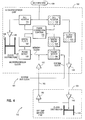
- FIG. 3 is a high-level block diagram illustrative of a self-synchronizing phase delay system 100 for coupling DLL's in accordance with a preferred embodiment of the present invention.
- System 100 is a self-synchronizing phase delay system for coupling DLL's , which causes phase adjustments of the digital-locked loops to occur simultaneously at a synchronization point.
- System 100 reduces the timing penalty for misaligned phase adjustment normally associated with independently operating DLL's. The normal penalty increases chip-to-chip path time.
- a SAW oscillator 104 sends a first reference signal to microprocessor chip 102 , which also receives a second reference signal from system bus clock 106 .
- An off-chip memory chip 108 is coupled to microprocessor 102 , which is also coupled to a system bus 20 .
- Microprocessor chip 102 is the physical realization of a CPU of a given - computer system on either a single semiconductor chip or on a small number of chips.
- microprocessor chip 102 can be a CPU such as CPU 22 depicted in FIG. 2 .
- Microprocessor chip 102 can also be included as part of a multi-chip microprocessor system, such as multi-chip uniprocessors, uniprocessors with off-chip memory, or multiprocessor configurations.
- a first reference signal, system bus clock 106 is provided to microprocessor chip 102 via bus lines.
- SAW oscillator 104 provides a second reference signal.
- SAW oscillator 104 can be a crystal oscillator based on an appropriate oscillation producing material such as quartz crystals.
- Off-chip memory chip 108 can provide extra memory, such as a cache memory area, for utilization with microprocessor chip 102 . Together, microprocessor 102 and off-chip memory chip 108 provide the basis of a multiprocessor.
- FIG. 4 is a more detailed block diagram illustrative of a self-synchronizing phase delay system 112 for coupling DLL's in accordance with a preferred embodiment of the present invention.
- SAW oscillator 104 is preferably an 800.4 MHz SAW oscillator.
- Microprocessor chip 102 includes a first DLL rotator 118 which receives the second reference signal, i.e., the signal from SAW oscillator 104 .
- a second DLL rotator 116 also receives the signal from SAW oscillator 104 .
- the rotators 116 and 118 generate a number of signals in response to the SAW oscillator input signal, which are used in turn as a source signal for a clock.
- four signals are generated by such a rotator.
- the first such signal generated by such a rotator leads the second signal by 1/4 cycle
- the second signal leads the third by 1/4 cycle
- the fourth signal leads the third by 1/4 cycle.
- One of the four signals is selected as a source signal at a time for output by such a rotator.
- the selection of source signals goes in sequence, wherein the second signal is selected following the first, the third signal is selected following the second, and so on.
- the term “rotate” is used to refer to a change in the selected source for the output signal from such a rotator, since the selection rotates among the four possible source signals in the 1-2-3-4-1-etc. sequence.
- stall is also used to refer to such a change in the selected source signal for outputing from such a rotator, since each of the four signals is 1/4 cycle behind the preceding signal, so that switching from the first signal to the second, and so forth substantially instantaneously introduces a 1/4 cycle shift in the rotator output in a lagging direction.
- First DLL rotator 118 provides a first clock signal to clock divider 130 , which reduces the frequency of the first clock signal by a predetermined multiple, such as by a multiple of two, to provide a "memory clock" signal, i.e., a clock signal for off-chip memory.
- Second DLL rotator 116 sends a second clock signal to buffer 126 , which in turn provides the buffered clock signal to clock distribution system 128 .
- Clock distribution system 128 distributes the buffered clock signal (the "microprocessor clock” signal) throughout the distribution system 128 .
- Output from phase correction control circuit 120 is input to first DLL rotator 118 and second DLL rotator 116 .
- a control signal from second phase detector 132 is fed to second digital filter 122 .
- a control signal from second digital filter 122 is fed to phase correction control circuit 120 .
- a control signal from first phase detector 134 is fed to first digital filter 124 .
- a control signal from first digital filter 124 is also fed to phase correction control circuit 120 .
- Second phase detector 132 receives the second clock signal from DLL Rotator 116 via clock distribution 128 .
- First phase detector 134 receives the first reference signal from system bus clock 106 .
- Buffer 136 provides the clock signal from divider 130 to second phase detector 132 and first phase detector 134 .
- Off-chip memory chip 108 includes a buffer 142 which receives the clock signal from divider 130 , via buffers 138 and 146 . Output from buffer 146 is also coupled to clock distribution system 148 .
- System 112 allows first and second clock signals from first and second DLL rotators 118 and 116 to be placed under coordinated control. That is, the first and second clock signals are fed back, including through the clock distribution path 128 and interchip paths (between the microprocessor and the off-chip memory), to control circuitry, so that the first and second clock signals can be synchronized to each other and the system bus clock 106 .
- the system bus clock and memory clock are phase locked as follows.
- First phase detector 134 detects a phase difference between the system bus clock and the memory clock, derived from the first clock as divided by bus divider 130 and delayed by interchip paths, and provides a control signal responsive to the measured phase error to digital filter 124 .
- the first digital filter integrates the error signal and provides a control signal responsive thereto to the phase correction control circuitry 120 , which controls stalling of the memory clock signal by the first rotator 118 .
- the microprocessor clock and memory clock are synchronized by rotating the source for the microprocessor clock each time a source for the memory clock also undergoes a rotation. That is, second phase detector 132 detects a phase difference between the microprocessor clock (i.e., DLL rotator 116 output) and the memory clock (i.e., DLL rotator 118 output) and provides a control signal responsive to the phase difference (i.e. error signal) to digital filter 122 .
- This second digital filter 122 integrates the error signal and provides a control signal responsive thereto to the phase correction control circuitry 120 , which controls stalling of the second (i.e. microprocessor) clock signal by the second rotator 116 .
- phase correction control circuitry 120 causes the memory clock rotator 118 to stall in response to the error signal from the microprocessor clock phase detector 132.
- a low frequency e.g. 1kHz
- the memory clock signal derived from the SAW oscillator and reduced in frequency by divide circuitry 130 is designed to be slightly faster than the system bus clock 106 .
- the SAW oscillator 104 , DLL rotator 118 , divide circuitry 130 , signal paths, phase detector 134 , digital filter 124 and phase correction controller 120 form a first DLL which stalls the memory clock as required so that the memory clock remains synchronized with the system bus clock.
- the rotator 118 generates a first plurality of signals, in response to the first reference signal from the SAW oscillator.
- the first plurality of signals have time-varying phase differences with respect to the second reference clock signal from the system bus clock.
- the SAW oscillator 104 , DLL rotator 116 , microprocessor clock paths, including distribution 128, phase detector 132 , digital filter 122 and phase correction controller 120 form a second DLL which stalls the microprocessor clock responsive to the microprocessor clock leading the memory clock. This synchronises the memory clock and the microprocessor clock when the microprocessor clock leads the memory clock.
- the rotator 116 generates a second plurality of signals, in response to the first reference signal from the SAW oscillator.
- the second plurality of signals have time-varying phase differences with respect to the second reference clock signal from the system bus clock.
- phase detector 134 and digital filter 124 form a third DLL, which stalls the memory clock responsive to the microprocessor clock lagging the memory clock. This synchronizes the memory clock and the microprocessor clock when the microprocessor clock lags the memory clock.
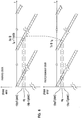
- clock phase error is shown as a function of time for a single DLL using a SAW oscillator.
- This example depicts a desired 400 MHz clock signal. Therefore, the phase error shown is a phase error relative to the desired 400 MHz target frequency.
- the first possible source signal is used as the source signal for the desired 400 MHz clock signal.
- the source for the clock signal is switched from the first possible source signal to the second possible source signal, from the second to the third, and so on.
- the phase error shown in FIG. 5 is generated by the selected source signal, and, as previously stated, is measured with respect to the target 400 MHz clock signal. That is, during the first interval shown, from t0 to t1, the source signal depicted is from the first possible source signal; during the second interval shown, from t1 to t2, the source signal depicted is from the second possible source signal; etc.
- FIG. 5 shows the 1.25 psec/cycle phase error slope as a band, 10 psec wide.
- 1/4 cycle (0.2/400 increasing phase error per cycle) * (500 cycles).
- the source signal is switched from the first possible source signal to the second. Since the second possible source signal is 1/4 phase behind the first, at 400.2 Mhz, this introduces a substantially instantaneous positive shift in phase error very slightly less than 1/4 cycle, i.e. a (400/400.2)/4 positive shift in phase error, so that the accumulated negative phase error is completely offset to within a margin much smaller than the inherent operating jitter.
- FIG. 6 depicts phase errors for the coupled memory clock and microprocessor bus clock which are synchronized as described in connection with FIG. 4.
- the intentionally introduced, increasing negative phase error, and instantaneous, though infrequent positive jitter, introduced once each 500 cycles, are synchronized for the two clock signals, so that their effect is not cumulative with respect to launching and capturing data in transfers between the microprocessor and memory. Therefore, only the inherent operating jitter, assumed to be 10 psec, plus the intentionally introduced constant 1.25 psec/cycle negative jitter reduces the cycle time available for such data transfers. Thus, the effective cycle time is reduced by only 11.25 psec
- phase error ea of the microprocessor clock at time ta is -100 psec, so that taking into account the 10 psec operating jitter, the phase error is in the range -95 to -105 psec.
- the phase error for the memory clock at time ta is in the same range, since the intentionally introduced phase error is synchronized with that of the microprocessor clock.
- the memory clock will capture the signal one cycle after the microprocessor launched it.
- the memory clock will have an intentionally introduced phase error, eb, at the time of capture which will be -101.25 psec, due to the intentionally introduced -1.25 psec phase error/cycle.
- the range of phase error for the memory clock at capture therefore, taking into account operating jitter, will be -96.25 to 106.25 psec.
- the worst case difference between phase error at launch and at capture will therefore be the difference between -95 psec and -106.25 psec phase error, i.e., 11.25 psec.
- the intentionally introduced phase error is synchronized for the two clocks, the result will be the same regardless of the choice of time ta.
Landscapes
- Engineering & Computer Science (AREA)
- Theoretical Computer Science (AREA)
- Physics & Mathematics (AREA)
- General Engineering & Computer Science (AREA)
- General Physics & Mathematics (AREA)
- Computer Networks & Wireless Communication (AREA)
- Signal Processing (AREA)
- Stabilization Of Oscillater, Synchronisation, Frequency Synthesizers (AREA)
- Synchronisation In Digital Transmission Systems (AREA)
Applications Claiming Priority (2)
| Application Number | Priority Date | Filing Date | Title |
|---|---|---|---|
| US09/004,136 US5949262A (en) | 1998-01-07 | 1998-01-07 | Method and apparatus for coupled phase locked loops |
| US4136 | 2007-12-19 |
Publications (2)
| Publication Number | Publication Date |
|---|---|
| EP0929155A2 true EP0929155A2 (de) | 1999-07-14 |
| EP0929155A3 EP0929155A3 (de) | 2002-07-17 |
Family
ID=21709351
Family Applications (1)
| Application Number | Title | Priority Date | Filing Date |
|---|---|---|---|
| EP98309761A Withdrawn EP0929155A3 (de) | 1998-01-07 | 1998-11-27 | Gekoppelte Phasenregelschleifen |
Country Status (7)
| Country | Link |
|---|---|
| US (1) | US5949262A (de) |
| EP (1) | EP0929155A3 (de) |
| JP (1) | JP3072733B2 (de) |
| KR (1) | KR19990066805A (de) |
| CN (1) | CN1225838C (de) |
| CA (1) | CA2254651A1 (de) |
| IL (1) | IL127401A0 (de) |
Cited By (1)
| Publication number | Priority date | Publication date | Assignee | Title |
|---|---|---|---|---|
| WO2007040734A1 (en) * | 2005-09-19 | 2007-04-12 | Ati Technologies, Inc. | Communicating client phase information in an io system |
Families Citing this family (24)
| Publication number | Priority date | Publication date | Assignee | Title |
|---|---|---|---|---|
| US6172937B1 (en) * | 1998-05-13 | 2001-01-09 | Intel Corporation | Multiple synthesizer based timing signal generation scheme |
| US6630855B2 (en) | 2001-03-29 | 2003-10-07 | Intel Corporation | Clock distribution phase alignment technique |
| US6504408B1 (en) | 2001-07-09 | 2003-01-07 | Broadcom Corporation | Method and apparatus to ensure DLL locking at minimum delay |
| DE10149512B4 (de) * | 2001-10-08 | 2006-08-03 | Infineon Technologies Ag | Verfahren und Vorrichtung zur Synchronisation der Datenübertragung zwischen zwei Schaltungen |
| US6611159B1 (en) | 2002-02-19 | 2003-08-26 | International Business Machines Corporation | Apparatus and method for synchronizing multiple circuits clocked at a divided phase locked loop frequency |
| US6809606B2 (en) * | 2002-05-02 | 2004-10-26 | Intel Corporation | Voltage ID based frequency control for clock generating circuit |
| US6885233B2 (en) * | 2002-05-02 | 2005-04-26 | Intel Corporation | Altering operating frequency and voltage set point of a circuit in response to the operating temperature and instantaneous operating voltage of the circuit |
| US6985041B2 (en) * | 2002-05-02 | 2006-01-10 | Intel Corporation | Clock generating circuit and method |
| US6737902B2 (en) * | 2002-05-16 | 2004-05-18 | Sun Microsystems, Inc. | Method and a system to distribute clock signals in digital circuits |
| JP3808026B2 (ja) * | 2002-10-23 | 2006-08-09 | 株式会社ルネサステクノロジ | 半導体装置 |
| KR100500929B1 (ko) | 2002-11-27 | 2005-07-14 | 주식회사 하이닉스반도체 | 지연 고정 루프 회로 |
| US20050084047A1 (en) * | 2003-09-30 | 2005-04-21 | Seiko Epson Corporation | Clock signal correcting circuit and communicating apparatus |
| KR100542696B1 (ko) | 2003-11-13 | 2006-01-11 | 주식회사 하이닉스반도체 | 반도체 장치의 리페어 퓨즈 박스 |
| KR100812600B1 (ko) * | 2005-09-29 | 2008-03-13 | 주식회사 하이닉스반도체 | 주파수가 다른 복수의 클럭을 사용하는 반도체메모리소자 |
| US7770049B1 (en) * | 2006-03-21 | 2010-08-03 | Advanced Micro Devices, Inc. | Controller for clock skew determination and reduction based on a lead count over multiple clock cycles |
| US7765425B1 (en) * | 2006-03-21 | 2010-07-27 | GlobalFoundries, Inc. | Incrementally adjustable skew and duty cycle correction for clock signals within a clock distribution network |
| US7518353B2 (en) * | 2006-04-07 | 2009-04-14 | Agilent Technologies, Inc. | Vector network analysis system and method using offset stimulus signals |
| US7991101B2 (en) * | 2006-12-20 | 2011-08-02 | Broadcom Corporation | Multiple channel synchronized clock generation scheme |
| US7975082B2 (en) * | 2007-07-12 | 2011-07-05 | Oracle America, Inc. | System and method to facilitate deterministic testing of data transfers between independent clock domains on a chip |
| TWI488095B (zh) * | 2009-02-26 | 2015-06-11 | Genesys Logic Inc | 省電之表面電容式觸控面板裝置以及其方法 |
| US8144529B2 (en) * | 2009-03-31 | 2012-03-27 | Intel Corporation | System and method for delay locked loop relock mode |
| US9160349B2 (en) * | 2009-08-27 | 2015-10-13 | Micron Technology, Inc. | Die location compensation |
| US8330644B2 (en) * | 2010-07-14 | 2012-12-11 | The United States Of America As Represented By The Administrator Of The National Aeronautics And Space Administration | Expandable and reconfigurable instrument node arrays |
| US8947377B2 (en) | 2011-04-06 | 2015-02-03 | Cypress Semiconductor Corporation | System and method for synchronization of touch panel devices |
Citations (4)
| Publication number | Priority date | Publication date | Assignee | Title |
|---|---|---|---|---|
| EP0445574A2 (de) * | 1990-03-05 | 1991-09-11 | Thinking Machines Corporation | Digitale Taktpufferschaltung mit regelbarer Verzögerung |
| US5150068A (en) * | 1988-08-10 | 1992-09-22 | Hitachi, Ltd. | Clock signal supply method and system |
| US5442776A (en) * | 1994-06-30 | 1995-08-15 | International Business Machines, Corp. | Electronically tuneable computer clocking system and method of electronically tuning distribution lines of a computer clocking system |
| US5631591A (en) * | 1995-05-30 | 1997-05-20 | National Semiconductor Corporation | Method and apparatus for synchronizing timing signals of two integrated circuit chips |
Family Cites Families (15)
| Publication number | Priority date | Publication date | Assignee | Title |
|---|---|---|---|---|
| DE2128824C3 (de) * | 1971-06-09 | 1974-03-07 | Linde Ag, 6200 Wiesbaden | Geklebter Plattenwärmetauscher |
| US4489289A (en) * | 1982-04-08 | 1984-12-18 | The United States Of America As Represented By The Secretary Of The Air Force | Saw oscillator with digital compensation for temperature related frequency changes |
| US4893271A (en) * | 1983-11-07 | 1990-01-09 | Motorola, Inc. | Synthesized clock microcomputer with power saving |
| US4715049A (en) * | 1986-03-12 | 1987-12-22 | American Telephone And Telegraph Company, At&T Bell Laboratories | Clock recovery and retiming scheme with saw filter phase trimming to achieve desired system phase adjustment |
| US4801818A (en) * | 1986-05-28 | 1989-01-31 | Siemens Aktiengesellschaft | Clock regeneration circuit |
| US5179574A (en) * | 1986-09-29 | 1993-01-12 | Kabushiki Kaisha Kenwood | Spread PN code signal receiver |
| US4903228A (en) * | 1988-11-09 | 1990-02-20 | International Business Machines Corporation | Single cycle merge/logic unit |
| US5166952A (en) * | 1990-05-24 | 1992-11-24 | Cylink Corporation | Method and apparatus for the reception and demodulation of spread spectrum radio signals |
| US5253268A (en) * | 1990-05-24 | 1993-10-12 | Cylink Corporation | Method and apparatus for the correlation of sample bits of spread spectrum radio signals |
| US5150078A (en) * | 1991-11-29 | 1992-09-22 | Hughes Aircraft Company | Low noise fine frequency step synthesizer |
| SE469616B (sv) * | 1991-12-23 | 1993-08-02 | Ellemtel Utvecklings Ab | Anordning foer foerskjutning av fasen hos en klocksignal samt saett och anordning foer taktaatervinning hos en digital datasignal |
| US5317284A (en) * | 1993-02-08 | 1994-05-31 | Hughes Aircraft Company | Wide band, low noise, fine step tuning, phase locked loop frequency synthesizer |
| US5544203A (en) * | 1993-02-17 | 1996-08-06 | Texas Instruments Incorporated | Fine resolution digital delay line with coarse and fine adjustment stages |
| US5349310A (en) * | 1993-06-09 | 1994-09-20 | Alcatel Network Systems, Inc. | Digitally controlled fractional frequency synthesizer |
| US5526380A (en) * | 1994-06-07 | 1996-06-11 | Texas Instruments Incorporated | First-order loop control configuration for a phase-rotator based clock synchronization circuit |
-
1998
- 1998-01-07 US US09/004,136 patent/US5949262A/en not_active Expired - Fee Related
- 1998-11-02 KR KR1019980046781A patent/KR19990066805A/ko active IP Right Grant
- 1998-11-26 CA CA002254651A patent/CA2254651A1/en not_active Abandoned
- 1998-11-27 EP EP98309761A patent/EP0929155A3/de not_active Withdrawn
- 1998-12-04 IL IL12740198A patent/IL127401A0/xx unknown
- 1998-12-07 CN CNB981230741A patent/CN1225838C/zh not_active Expired - Fee Related
-
1999
- 1999-01-04 JP JP11000049A patent/JP3072733B2/ja not_active Expired - Lifetime
Patent Citations (4)
| Publication number | Priority date | Publication date | Assignee | Title |
|---|---|---|---|---|
| US5150068A (en) * | 1988-08-10 | 1992-09-22 | Hitachi, Ltd. | Clock signal supply method and system |
| EP0445574A2 (de) * | 1990-03-05 | 1991-09-11 | Thinking Machines Corporation | Digitale Taktpufferschaltung mit regelbarer Verzögerung |
| US5442776A (en) * | 1994-06-30 | 1995-08-15 | International Business Machines, Corp. | Electronically tuneable computer clocking system and method of electronically tuning distribution lines of a computer clocking system |
| US5631591A (en) * | 1995-05-30 | 1997-05-20 | National Semiconductor Corporation | Method and apparatus for synchronizing timing signals of two integrated circuit chips |
Cited By (2)
| Publication number | Priority date | Publication date | Assignee | Title |
|---|---|---|---|---|
| WO2007040734A1 (en) * | 2005-09-19 | 2007-04-12 | Ati Technologies, Inc. | Communicating client phase information in an io system |
| US7509515B2 (en) | 2005-09-19 | 2009-03-24 | Ati Technologies, Inc. | Method and system for communicated client phase information during an idle period of a data bus |
Also Published As
| Publication number | Publication date |
|---|---|
| CN1222790A (zh) | 1999-07-14 |
| KR19990066805A (ko) | 1999-08-16 |
| IL127401A0 (en) | 1999-10-28 |
| EP0929155A3 (de) | 2002-07-17 |
| JP3072733B2 (ja) | 2000-08-07 |
| US5949262A (en) | 1999-09-07 |
| CN1225838C (zh) | 2005-11-02 |
| JPH11259167A (ja) | 1999-09-24 |
| CA2254651A1 (en) | 1999-07-07 |
Similar Documents
| Publication | Publication Date | Title |
|---|---|---|
| US5949262A (en) | Method and apparatus for coupled phase locked loops | |
| EP1179236B1 (de) | System und verfahren zur bereitstellung von phasenausgeglichenen master- und slavetaktsignalen | |
| JP4308436B2 (ja) | クロック位相シフターを有する遅延ロックループ | |
| CA2424702C (en) | Synchronized multi-output digital clock manager | |
| US7423462B2 (en) | Clock capture in clock synchronization circuitry | |
| US20020079937A1 (en) | Digital delay locked loop with wide dynamic range and fine precision | |
| US8269544B2 (en) | Power-supply noise suppression using a frequency-locked loop | |
| US6608530B1 (en) | Enhanced ZDB feedback methodology utilizing binary weighted techniques | |
| US6211739B1 (en) | Microprocessor controlled frequency lock loop for use with an external periodic signal | |
| US7151398B2 (en) | Clock signal generators having programmable full-period clock skew control | |
| KR100195855B1 (ko) | 소수배 시스템에 있어서 클록 동기 체계 | |
| JP2002171247A (ja) | 異機種混合コンピュータ・システムにおけるノード同期化の方法及び装置 | |
| US20040193931A1 (en) | System and method for transferring data from a first clock domain to a second clock domain | |
| US20050259505A1 (en) | System and method for maintaining device operation during clock signal adjustments | |
| CN101018049B (zh) | 延迟锁相回路 | |
| US6477657B1 (en) | Circuit for I/O clock generation | |
| EP1404020B1 (de) | Phasenregelkreis zum Reduzieren des Phasenfehlers im stationären Zustand | |
| US7100065B2 (en) | Controller arrangement for synchronizer data transfer between a core clock domain and bus clock domain each having its own individual synchronizing controller | |
| US6977539B1 (en) | Clock signal generators having programmable full-period clock skew control and methods of generating clock signals having programmable skews | |
| EP1618461B1 (de) | Deskew-system in einem taktverteilungsnetzwerk mit einem pll und einem dll | |
| US7219251B2 (en) | Programmable clock synchronizer | |
| US5870592A (en) | Clock generation apparatus and method for CMOS microprocessors using a differential saw oscillator | |
| EP0610052B1 (de) | Verfahren und Gerät zur Taktsteuerung | |
| US6516006B1 (en) | Self-adjusting clock phase controlled architecture | |
| JPH0879556A (ja) | コントローラチップのデータ信号同期化方法および回路 |
Legal Events
| Date | Code | Title | Description |
|---|---|---|---|
| PUAI | Public reference made under article 153(3) epc to a published international application that has entered the european phase |
Free format text: ORIGINAL CODE: 0009012 |
|
| AK | Designated contracting states |
Kind code of ref document: A2 Designated state(s): AT BE CH CY DE DK ES FI FR GB GR IE IT LI LU MC NL PT SE |
|
| AX | Request for extension of the european patent |
Free format text: AL;LT;LV;MK;RO;SI |
|
| PUAL | Search report despatched |
Free format text: ORIGINAL CODE: 0009013 |
|
| AK | Designated contracting states |
Kind code of ref document: A3 Designated state(s): AT BE CH CY DE DK ES FI FR GB GR IE IT LI LU MC NL PT SE |
|
| AX | Request for extension of the european patent |
Free format text: AL;LT;LV;MK;RO;SI |
|
| AKX | Designation fees paid | ||
| REG | Reference to a national code |
Ref country code: DE Ref legal event code: 8566 |
|
| STAA | Information on the status of an ep patent application or granted ep patent |
Free format text: STATUS: THE APPLICATION IS DEEMED TO BE WITHDRAWN |
|
| 18D | Application deemed to be withdrawn |
Effective date: 20030118 |