EP0929109B1 - Method for manufacturing a semiconductor light emitting device - Google Patents
Method for manufacturing a semiconductor light emitting device Download PDFInfo
- Publication number
- EP0929109B1 EP0929109B1 EP99100082A EP99100082A EP0929109B1 EP 0929109 B1 EP0929109 B1 EP 0929109B1 EP 99100082 A EP99100082 A EP 99100082A EP 99100082 A EP99100082 A EP 99100082A EP 0929109 B1 EP0929109 B1 EP 0929109B1
- Authority
- EP
- European Patent Office
- Prior art keywords
- nitride semiconductor
- layer
- type iii
- mask
- annealing process
- Prior art date
- Legal status (The legal status is an assumption and is not a legal conclusion. Google has not performed a legal analysis and makes no representation as to the accuracy of the status listed.)
- Expired - Lifetime
Links
- 239000004065 semiconductor Substances 0.000 title claims description 65
- 238000000034 method Methods 0.000 title claims description 61
- 238000004519 manufacturing process Methods 0.000 title claims description 13
- 230000008569 process Effects 0.000 claims description 34
- 229910052739 hydrogen Inorganic materials 0.000 claims description 28
- 150000004767 nitrides Chemical class 0.000 claims description 27
- 239000001257 hydrogen Substances 0.000 claims description 26
- 229910052751 metal Inorganic materials 0.000 claims description 25
- 239000002184 metal Substances 0.000 claims description 25
- 238000000137 annealing Methods 0.000 claims description 23
- UFHFLCQGNIYNRP-UHFFFAOYSA-N Hydrogen Chemical compound [H][H] UFHFLCQGNIYNRP-UHFFFAOYSA-N 0.000 claims description 19
- VYPSYNLAJGMNEJ-UHFFFAOYSA-N Silicium dioxide Chemical compound O=[Si]=O VYPSYNLAJGMNEJ-UHFFFAOYSA-N 0.000 claims description 10
- 239000000758 substrate Substances 0.000 claims description 9
- IJGRMHOSHXDMSA-UHFFFAOYSA-N Atomic nitrogen Chemical compound N#N IJGRMHOSHXDMSA-UHFFFAOYSA-N 0.000 claims description 8
- 229910052681 coesite Inorganic materials 0.000 claims description 5
- 229910052906 cristobalite Inorganic materials 0.000 claims description 5
- 239000000377 silicon dioxide Substances 0.000 claims description 5
- 229910052682 stishovite Inorganic materials 0.000 claims description 5
- 229910052905 tridymite Inorganic materials 0.000 claims description 5
- 230000003213 activating effect Effects 0.000 claims description 4
- 229910052737 gold Inorganic materials 0.000 claims description 4
- 230000000415 inactivating effect Effects 0.000 claims description 4
- 229910052757 nitrogen Inorganic materials 0.000 claims description 4
- 229910052697 platinum Inorganic materials 0.000 claims description 4
- 229910052759 nickel Inorganic materials 0.000 claims description 3
- 150000004678 hydrides Chemical class 0.000 claims description 2
- 229910002601 GaN Inorganic materials 0.000 description 21
- 125000004429 atom Chemical group 0.000 description 13
- 239000011777 magnesium Substances 0.000 description 7
- -1 nitride compound Chemical class 0.000 description 7
- 229910002704 AlGaN Inorganic materials 0.000 description 6
- 238000005530 etching Methods 0.000 description 6
- 150000001875 compounds Chemical class 0.000 description 5
- 238000002347 injection Methods 0.000 description 4
- 239000007924 injection Substances 0.000 description 4
- 239000002243 precursor Substances 0.000 description 4
- 229910003828 SiH3 Inorganic materials 0.000 description 3
- 230000004888 barrier function Effects 0.000 description 3
- 238000005253 cladding Methods 0.000 description 3
- 239000007789 gas Substances 0.000 description 3
- 150000002431 hydrogen Chemical class 0.000 description 3
- 229910052749 magnesium Inorganic materials 0.000 description 3
- 230000003647 oxidation Effects 0.000 description 3
- 238000007254 oxidation reaction Methods 0.000 description 3
- 230000035699 permeability Effects 0.000 description 3
- JLTRXTDYQLMHGR-UHFFFAOYSA-N trimethylaluminium Chemical compound C[Al](C)C JLTRXTDYQLMHGR-UHFFFAOYSA-N 0.000 description 3
- XCZXGTMEAKBVPV-UHFFFAOYSA-N trimethylgallium Chemical compound C[Ga](C)C XCZXGTMEAKBVPV-UHFFFAOYSA-N 0.000 description 3
- 229910052799 carbon Inorganic materials 0.000 description 2
- 239000013256 coordination polymer Substances 0.000 description 2
- AXAZMDOAUQTMOW-UHFFFAOYSA-N dimethylzinc Chemical compound C[Zn]C AXAZMDOAUQTMOW-UHFFFAOYSA-N 0.000 description 2
- 239000002019 doping agent Substances 0.000 description 2
- 238000001312 dry etching Methods 0.000 description 2
- 230000008020 evaporation Effects 0.000 description 2
- 238000001704 evaporation Methods 0.000 description 2
- 125000005842 heteroatom Chemical group 0.000 description 2
- 239000012535 impurity Substances 0.000 description 2
- 229910052738 indium Inorganic materials 0.000 description 2
- 239000012774 insulation material Substances 0.000 description 2
- 239000012212 insulator Substances 0.000 description 2
- 150000002739 metals Chemical class 0.000 description 2
- 229910052763 palladium Inorganic materials 0.000 description 2
- 238000000206 photolithography Methods 0.000 description 2
- 238000001020 plasma etching Methods 0.000 description 2
- 229910052594 sapphire Inorganic materials 0.000 description 2
- 239000010980 sapphire Substances 0.000 description 2
- IBEFSUTVZWZJEL-UHFFFAOYSA-N trimethylindium Chemical compound C[In](C)C IBEFSUTVZWZJEL-UHFFFAOYSA-N 0.000 description 2
- 238000001039 wet etching Methods 0.000 description 2
- 229910052725 zinc Inorganic materials 0.000 description 2
- 208000019901 Anxiety disease Diseases 0.000 description 1
- JMASRVWKEDWRBT-UHFFFAOYSA-N Gallium nitride Chemical compound [Ga]#N JMASRVWKEDWRBT-UHFFFAOYSA-N 0.000 description 1
- FYYHWMGAXLPEAU-UHFFFAOYSA-N Magnesium Chemical compound [Mg] FYYHWMGAXLPEAU-UHFFFAOYSA-N 0.000 description 1
- 229910052782 aluminium Inorganic materials 0.000 description 1
- 230000036506 anxiety Effects 0.000 description 1
- 229910052785 arsenic Inorganic materials 0.000 description 1
- 230000000903 blocking effect Effects 0.000 description 1
- 238000006555 catalytic reaction Methods 0.000 description 1
- 238000005229 chemical vapour deposition Methods 0.000 description 1
- 238000010276 construction Methods 0.000 description 1
- 238000007796 conventional method Methods 0.000 description 1
- PMHQVHHXPFUNSP-UHFFFAOYSA-M copper(1+);methylsulfanylmethane;bromide Chemical compound Br[Cu].CSC PMHQVHHXPFUNSP-UHFFFAOYSA-M 0.000 description 1
- 238000002474 experimental method Methods 0.000 description 1
- APFVFJFRJDLVQX-UHFFFAOYSA-N indium atom Chemical compound [In] APFVFJFRJDLVQX-UHFFFAOYSA-N 0.000 description 1
- UIUXUFNYAYAMOE-UHFFFAOYSA-N methylsilane Chemical compound [SiH3]C UIUXUFNYAYAMOE-UHFFFAOYSA-N 0.000 description 1
- 230000010355 oscillation Effects 0.000 description 1
- 229910052698 phosphorus Inorganic materials 0.000 description 1
- 230000005855 radiation Effects 0.000 description 1
- 230000009257 reactivity Effects 0.000 description 1
- 230000009467 reduction Effects 0.000 description 1
- 239000000243 solution Substances 0.000 description 1
Images


Classifications
-
- H—ELECTRICITY
- H10—SEMICONDUCTOR DEVICES; ELECTRIC SOLID-STATE DEVICES NOT OTHERWISE PROVIDED FOR
- H10H—INORGANIC LIGHT-EMITTING SEMICONDUCTOR DEVICES HAVING POTENTIAL BARRIERS
- H10H20/00—Individual inorganic light-emitting semiconductor devices having potential barriers, e.g. light-emitting diodes [LED]
- H10H20/01—Manufacture or treatment
- H10H20/011—Manufacture or treatment of bodies, e.g. forming semiconductor layers
- H10H20/013—Manufacture or treatment of bodies, e.g. forming semiconductor layers having light-emitting regions comprising only Group III-V materials
- H10H20/0133—Manufacture or treatment of bodies, e.g. forming semiconductor layers having light-emitting regions comprising only Group III-V materials with a substrate not being Group III-V materials
- H10H20/01335—Manufacture or treatment of bodies, e.g. forming semiconductor layers having light-emitting regions comprising only Group III-V materials with a substrate not being Group III-V materials the light-emitting regions comprising nitride materials
Definitions
- the present invention relates to a method for manufacturing a light emitting device.
- III-V nitride semiconductors gallium nitride and related compound semiconductors
- III-V nitride semiconductor is defined as the semiconductor of the compound of GaN of III group atom with N of V group atom, the compound of Ga of III group atom with another III group atom such as Al, In and others which is substituted for a part of Ga, and the compound of N of V group atom with another V group atom such as P, As and others which is substituted for a part of N.
- the method by the wet etching can not be used, because an etching solution suitable for the semiconductor of the GaN related compound is not yet discovered.
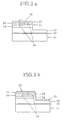
- a semiconductor light emitting device of Fig. 3a has a layer structure comprising a III-V nitride semiconductor on a substrate 21, which comprises an n-type buffer layer 22, n-type GaN clad layer 23, n-type AlGaN clad layer 24, InGaN active layer 25, p-type clad layer 26, and p-type GaN contact layer 27.
- the entire semiconductor layer is annealing-processed, thereby activating the p-type layers.
- a mask 28 of insulation material is mounted on the surface of the p-type contact layer 27, and the semiconductor is annealing-processed in an ambience of hydrogen.
- p-type layers 29 not covered by the mask 28 are made high resistance to form a narrow electric current path as shown in Fig. 3a.
- the mask 28 is removed and a p-electrode 30 of Au is mounted on a current injection area of the p-type contact layer 27 as shown in Fig. 3b.
- the n-type clad layer 23 is exposed by etching a part of the semiconductor layer (Fig. 3a), and an n-electrode 31 of Au is mounted on the surface of the n-type clad layer 23, thereby forming a semiconductor light emitting device (Fig. 3b).
- the mask 28 of insulation material must be removed, and the removed portion is exposed in the atmosphere.
- the exposed portion is oxidized to form an oxidation film on the portion.
- the semiconductor layer is annealing-processed again. As a result, hydrogen diffuses from the high resistance portion to the low resistance portion of the narrow path, thereby increasing the resistance of the narrow path.
- the document EP-A-0 723 303 describes a method in which a reflecting mirror is used as a mask blocking the radiation of an excimer laser, which anneals the exposed part of the p-type layer.
- An object of the present invention is to provide a method for making a semiconductor light emitting device which may easily form an electric current injection area, easily manufacture the light emitting device in the mass production, and reduce the contact resistance with the electrode.
- a method for manufacturing a semiconductor light emitting device having a stack structure which consists of at least an n-type III-V nitride semiconductor layer, an active layer, and a p-type III-V nitride semiconductor layer on a substrate.
- the method is set out in appended claims 1 an 2 and comprises the steps of a first annealing process for the purpose of activating the p-type III-V nitride semiconductor layer, forming a metal mask of one of Ni, Pt, and Au or a mask of a Pd film with a film non-permeable for hydrogen thereon on the area of the III-V nitride semiconductor area where electric current is to be injected, a second annealing process for inactivating the p-type III-V nitride semiconductor layer except for the masked area.
- the film on the Pd film which is not permeable for hydrogen, can be SiO 2 .
- the first annealing process can be performed in an ambience of nitrogen, and the second annealing process can be performed in an ambience including hydrogen or hydrides.
- the method preferably further comprises forming an n-electrode on the n-type III-V nitride semiconductor layer after the second annealing process.
- the semiconductor device comprises a III-V nitride compound semiconductor grown on a substrate 1 of sapphire.
- the semiconductor comprises a low temperature buffer layer 2 of aluminum nitride (hereinafter called AlN), clad layer 3 of n-type GaN in which Si is doped, clad layer 4 of n-type AlGaN in which Si is doped, active layer 5 of In(indium)GaN, clad layer 6 of p-type AlGaN in which Mg is doped, contact layer 7 of p-type GaN in which Mg is doped.
- AlN aluminum nitride
- an atom of 4A group such as C, Ge may be used other than Si
- an atom of 2A group atom such as Be, Ca and others and an atom of 2B group atom such as Zn may be used.
- the substrate 1 of sapphire is loaded in a reactor of the MOCVD (Metal Organic Chemical Vapor Deposition) and held in a hydrogen flow at 1050°C for ten minutes, so that the surface of the substrate 1 is heat-cleaned. Subsequently the temperature of the substrate 1 is reduced to 600°C, and NH 3 as a nitrogen precursor and TMA (trimethyl aluminium) as an Al precursor are introduced in the reactor, so that the buffer layer 2 of AlN is grown on the substrate 1 in the thickness of 0.05 ⁇ m.
- MOCVD Metal Organic Chemical Vapor Deposition
- the n-type clad layer is grown between 700°C and 1200°C using NH 3 and TMG (trimethyl gallium) as precursors, the thickness is 2 ⁇ m.
- TMG trimethyl gallium
- Me-SiH 3 methyl silane
- n-type AlGaN cladding layer 4 is grown about 0.2 ⁇ m thick.
- TMI trimethyl indium
- TMG trimethyl indium
- NH 3 trimethyl indium
- the p-type AlGaN cladding layer 6 is grown by use of identical gases of n-type cladding layer except for Me-SiH 3 , and CP 2 Mg (biscyclopentadiniel magnesium) or DMZn (dimethylzinc).
- the p-type GaN contact layer 7 is grown about 0.2 ⁇ m thick using identical gases of n-type GaN layer 3 except for Me-SiH 3 , and CP 2 Mg or DEZn.
- each layer of the III-V nitride semiconductor is laminated.
- the p-type semiconductor layers 6 and 7 in Fig. 2a are high resistance. Therefore, first of all the resistance lowering process of the p-type semiconductor layers 6 and 7 are carried out.
- an etching process is performed in order to expose the n-electrode.
- an etching mask is formed by the general photolithography, unnecessary portions of the p-type GaN layers are removed by the RIE (Reactive Ion Etching), thereby partially exposing the n-type GaN layer 3 (Fig. 2b).
- This process is not necessary when the n-electrode is to be exposed at another part. Furthermore, the removing process is not necessarily firstly performed.
- a first annealing process is carried out as follows in order to reduce the resistance.
- the entire semiconductor layer is put in a nitrogen ambience at about 800°C for about 20 minutes, so that the p-type layers are activated to reduce the resistance due to the division of the combination of Mg, Zn and H which are dobants in the p-type layer.
- a metal mask 8 is formed on the contact layer 7 to cover a portion which is to be a current introducing area.
- the metal mask 8 has a shape of stripe having a width of 2 to 20 ⁇ m.
- the metal mask is formed by the photolithography, using one of Ni, Pt, Pd and Au each of which has a large work function.
- a metal having not hydrogen permeability and having a good characteristic in electrical contact with the semiconductor layer of the p-type GaN it is preferable to use a metal having not hydrogen permeability and having a good characteristic in electrical contact with the semiconductor layer of the p-type GaN.
- Pd has hydrogen permeability, it can be used by overlaying a film having not hydrogen permeability such as SiO 2 .
- the hydrogen or hydrogen compound is dissolved by the catalysis on the surface of the mask at the annealing process so that excessive active hydrogen generates, which results in increase of the active hydrogen density in the ambience at the annealing process.
- the excessive active hydrogen diffuses in the underside of the metal mask, where is to be kept at low resistance. Consequently the portion may be made high resistance.
- a second annealing process is carried out, wherein the entire semiconductor having the metal mask 8 is annealing-processed in an ambience including hydrogen or a hydrogen compound at about 800°C for about 15 minutes.
- the hydrogen in the ambience enters the semiconductor of the p-type layer, thereby combining Mg, Zn and H which are dopants in the p-type layer, and inactivating the p-type layer designated by a reference numeral 9 in Fig. 2c, causing it to increase the resistance to a high value (10 5 ⁇ cm).
- the p-type layer covered by the mask 8 is maintained at a low resistance.
- a p-electrode 10 covers the metal mask 8 and the contact layer 7.
- the p-electrode 10 has a stripe shape having a width of about 200 ⁇ m larger than the above described width of the metal mask 8, and is formed by the evaporation of Ni at thickness 50 nm and Au at thickness 200 nm.
- an electrode 11 is overlaid.
- the electrode 11 is formed by the evaporation of C, Ge of 50 nm in thickness and Al of 200 nm in thickness.
- the III-V nitride semiconductor device is manufactured.
- the contact resistance between the metal mask and the p-type contact layer 7 is reduced by the annealing process.
- the electrode is evaporated after the removing of the mask, thereby the surface of the semiconductor is exposed to the atmosphere. Consequently, the surface is promptly oxidized.
- the oxidized film is an insulator, the film obstructs the injection of the electric current.
- an electrode is formed on the surface.
- the oxidized film can not perfectively be removed.
- the surface is oxidized again. As a result, an oxidized film inevitably exists between the electrode and the GaN semiconductor. This is one of reasons increasing the contact resistance.
- the mask since the mask is not removed, it is possible to prevent the oxidation after the removing of the mask. Also in the present invention, the oxidation before the forming of the mask can not be avoided. However, the film is very thin. Therefore it is considered that the metal of the mask penetrates the oxidized film and contacts directly with the III-V nitride semiconductor of the under layer, as a result it is possible to inject the electric current.
- the process for removing the mask is unnecessary. Accordingly, it is possible to manufacture the semiconductor light emitting device at minimum steps of the process.
- the electric current injection area can be restricted by a simple method, the semiconductor can be manufactured in the mass production. In addition, it is possible to obtain the semiconductor device having low contact resistance.
- the present invention may be applied to other junction structures such as the pn homo-junction diode, separate confinement hetero structure, and others, and to the manufacture of the unipolar transistor such as FET.
- the current path restriction structure can be found by the annealing process. Therefore the present invention is suitable for simplifying the manufacturing apparatus. By using the metal mask as the electrode, the resistance of the device is reduced, thereby increasing the device characteristic.
Landscapes
- Led Devices (AREA)
- Semiconductor Lasers (AREA)
- Electrodes Of Semiconductors (AREA)
Applications Claiming Priority (2)
| Application Number | Priority Date | Filing Date | Title |
|---|---|---|---|
| JP1320498A JPH11204833A (ja) | 1998-01-08 | 1998-01-08 | 半導体発光素子の製造方法 |
| JP1320498 | 1998-01-08 |
Publications (2)
| Publication Number | Publication Date |
|---|---|
| EP0929109A1 EP0929109A1 (en) | 1999-07-14 |
| EP0929109B1 true EP0929109B1 (en) | 2004-11-24 |
Family
ID=11826636
Family Applications (1)
| Application Number | Title | Priority Date | Filing Date |
|---|---|---|---|
| EP99100082A Expired - Lifetime EP0929109B1 (en) | 1998-01-08 | 1999-01-05 | Method for manufacturing a semiconductor light emitting device |
Country Status (4)
| Country | Link |
|---|---|
| US (1) | US6200827B1 (enExample) |
| EP (1) | EP0929109B1 (enExample) |
| JP (1) | JPH11204833A (enExample) |
| DE (1) | DE69922061T2 (enExample) |
Cited By (1)
| Publication number | Priority date | Publication date | Assignee | Title |
|---|---|---|---|---|
| US8704240B2 (en) | 2004-06-30 | 2014-04-22 | Cree, Inc. | Light emitting devices having current reducing structures |
Families Citing this family (9)
| Publication number | Priority date | Publication date | Assignee | Title |
|---|---|---|---|---|
| US6727167B2 (en) | 2000-10-13 | 2004-04-27 | Emcore Corporation | Method of making an aligned electrode on a semiconductor structure |
| US20060002442A1 (en) * | 2004-06-30 | 2006-01-05 | Kevin Haberern | Light emitting devices having current blocking structures and methods of fabricating light emitting devices having current blocking structures |
| US7335920B2 (en) | 2005-01-24 | 2008-02-26 | Cree, Inc. | LED with current confinement structure and surface roughening |
| JP4830619B2 (ja) * | 2006-05-10 | 2011-12-07 | 住友電気工業株式会社 | 集積半導体光素子およびその製造方法 |
| TW201005994A (en) * | 2008-07-23 | 2010-02-01 | Walsin Lihwa Corp | Light emitting diode and the method for manufacturing the same |
| US8592309B2 (en) * | 2009-11-06 | 2013-11-26 | Ultratech, Inc. | Laser spike annealing for GaN LEDs |
| JP2013120936A (ja) | 2011-12-07 | 2013-06-17 | Ultratech Inc | パターン効果を低減したGaNLEDのレーザーアニール |
| JP6561367B2 (ja) * | 2014-02-26 | 2019-08-21 | 学校法人 名城大学 | npn型窒化物半導体発光素子の製造方法 |
| US10700239B1 (en) * | 2019-03-21 | 2020-06-30 | Mikro Mesa Technology Co., Ltd. | Micro light-emitting diode |
Family Cites Families (4)
| Publication number | Priority date | Publication date | Assignee | Title |
|---|---|---|---|---|
| US5751013A (en) * | 1994-07-21 | 1998-05-12 | Matsushita Electric Industrial Co., Ltd. | Semiconductor light-emitting device and production method thereof |
| JPH0888432A (ja) * | 1994-09-16 | 1996-04-02 | Rohm Co Ltd | 半導体レーザの製法 |
| JP3254931B2 (ja) * | 1994-10-17 | 2002-02-12 | 松下電器産業株式会社 | p型窒化ガリウム系化合物半導体の製造方法 |
| JPH08222797A (ja) * | 1995-01-17 | 1996-08-30 | Hewlett Packard Co <Hp> | 半導体装置およびその製造方法 |
-
1998
- 1998-01-08 JP JP1320498A patent/JPH11204833A/ja active Pending
-
1999
- 1999-01-04 US US09/224,356 patent/US6200827B1/en not_active Expired - Lifetime
- 1999-01-05 DE DE69922061T patent/DE69922061T2/de not_active Expired - Lifetime
- 1999-01-05 EP EP99100082A patent/EP0929109B1/en not_active Expired - Lifetime
Cited By (1)
| Publication number | Priority date | Publication date | Assignee | Title |
|---|---|---|---|---|
| US8704240B2 (en) | 2004-06-30 | 2014-04-22 | Cree, Inc. | Light emitting devices having current reducing structures |
Also Published As
| Publication number | Publication date |
|---|---|
| DE69922061D1 (de) | 2004-12-30 |
| JPH11204833A (ja) | 1999-07-30 |
| US6200827B1 (en) | 2001-03-13 |
| DE69922061T2 (de) | 2005-11-24 |
| EP0929109A1 (en) | 1999-07-14 |
Similar Documents
| Publication | Publication Date | Title |
|---|---|---|
| US7760785B2 (en) | Group-III nitride semiconductor device | |
| JP3688843B2 (ja) | 窒化物系半導体素子の製造方法 | |
| US6020602A (en) | GaN based optoelectronic device and method for manufacturing the same | |
| JP2540791B2 (ja) | p型窒化ガリウム系化合物半導体の製造方法。 | |
| JP3408413B2 (ja) | 半導体の製造方法及び半導体装置 | |
| US7714350B2 (en) | Gallium nitride based semiconductor device and method of manufacturing same | |
| EP0828302B1 (en) | Gallium nitride group compound semiconductor light-emitting device and method for fabricating the same | |
| KR100303963B1 (ko) | 질화갈륨계화합물반도체발광소자및그제조방법 | |
| JP2002198314A (ja) | 窒化物半導体の製造方法、窒化物半導体素子の製造方法及びそれを用いた窒化物半導体素子 | |
| JP3325479B2 (ja) | 化合物半導体素子及びその製造方法 | |
| JP2000286449A (ja) | Iii族窒化物系化合物半導体素子及びその製造方法 | |
| US10685835B2 (en) | III-nitride tunnel junction with modified P-N interface | |
| KR20040104959A (ko) | 도핑된 그룹 ⅲ-ⅴ 질화물 재료 및 이를 포함하는마이크로일렉트로닉 디바이스 및 디바이스 프리커서 구조물 | |
| EP0929109B1 (en) | Method for manufacturing a semiconductor light emitting device | |
| JP2004172189A (ja) | 窒化物系半導体装置及びその製造方法 | |
| US6730938B2 (en) | Semiconductor light emitting device and method for manufacturing the same | |
| US5953581A (en) | Methods for manufacturing group III nitride compound semiconductor laser diodes | |
| JP3361964B2 (ja) | 半導体発光素子およびその製造方法 | |
| JP2803791B2 (ja) | 半導体素子の製造方法 | |
| JP3776538B2 (ja) | 半導体発光素子およびその製法 | |
| JP2790235B2 (ja) | 窒化ガリウム系化合物半導体のp型化方法 | |
| JPH11224859A (ja) | 窒化ガリウム系化合物半導体のドーピング方法および半導体素子の製造方法 | |
| JP2785253B2 (ja) | 窒化ガリウム系化合物半導体のp型化方法 | |
| US7320898B2 (en) | Semiconductor laser device and method for fabricating the same | |
| JP3347633B2 (ja) | 半導体素子およびその製造方法 |
Legal Events
| Date | Code | Title | Description |
|---|---|---|---|
| PUAI | Public reference made under article 153(3) epc to a published international application that has entered the european phase |
Free format text: ORIGINAL CODE: 0009012 |
|
| AK | Designated contracting states |
Kind code of ref document: A1 Designated state(s): DE FR GB |
|
| AX | Request for extension of the european patent |
Free format text: AL;LT;LV;MK;RO;SI |
|
| 17P | Request for examination filed |
Effective date: 19990701 |
|
| AKX | Designation fees paid |
Free format text: DE FR GB |
|
| 17Q | First examination report despatched |
Effective date: 20030403 |
|
| GRAP | Despatch of communication of intention to grant a patent |
Free format text: ORIGINAL CODE: EPIDOSNIGR1 |
|
| RIC1 | Information provided on ipc code assigned before grant |
Ipc: 7H 01S 5/32 B Ipc: 7H 01L 33/00 A |
|
| GRAS | Grant fee paid |
Free format text: ORIGINAL CODE: EPIDOSNIGR3 |
|
| GRAA | (expected) grant |
Free format text: ORIGINAL CODE: 0009210 |
|
| AK | Designated contracting states |
Kind code of ref document: B1 Designated state(s): DE FR GB |
|
| REG | Reference to a national code |
Ref country code: GB Ref legal event code: FG4D |
|
| REF | Corresponds to: |
Ref document number: 69922061 Country of ref document: DE Date of ref document: 20041230 Kind code of ref document: P |
|
| REG | Reference to a national code |
Ref country code: GB Ref legal event code: 746 Effective date: 20041216 |
|
| PLBE | No opposition filed within time limit |
Free format text: ORIGINAL CODE: 0009261 |
|
| STAA | Information on the status of an ep patent application or granted ep patent |
Free format text: STATUS: NO OPPOSITION FILED WITHIN TIME LIMIT |
|
| 26N | No opposition filed |
Effective date: 20050825 |
|
| ET | Fr: translation filed | ||
| REG | Reference to a national code |
Ref country code: FR Ref legal event code: D6 |
|
| REG | Reference to a national code |
Ref country code: GB Ref legal event code: 732E Free format text: REGISTERED BETWEEN 20090129 AND 20090204 |
|
| REG | Reference to a national code |
Ref country code: FR Ref legal event code: TP Ref country code: FR Ref legal event code: CD |
|
| PGFP | Annual fee paid to national office [announced via postgrant information from national office to epo] |
Ref country code: DE Payment date: 20131231 Year of fee payment: 16 |
|
| PGFP | Annual fee paid to national office [announced via postgrant information from national office to epo] |
Ref country code: FR Payment date: 20140108 Year of fee payment: 16 |
|
| PGFP | Annual fee paid to national office [announced via postgrant information from national office to epo] |
Ref country code: GB Payment date: 20140102 Year of fee payment: 16 |
|
| REG | Reference to a national code |
Ref country code: DE Ref legal event code: R119 Ref document number: 69922061 Country of ref document: DE |
|
| GBPC | Gb: european patent ceased through non-payment of renewal fee |
Effective date: 20150105 |
|
| PG25 | Lapsed in a contracting state [announced via postgrant information from national office to epo] |
Ref country code: GB Free format text: LAPSE BECAUSE OF NON-PAYMENT OF DUE FEES Effective date: 20150105 Ref country code: DE Free format text: LAPSE BECAUSE OF NON-PAYMENT OF DUE FEES Effective date: 20150801 |
|
| REG | Reference to a national code |
Ref country code: FR Ref legal event code: ST Effective date: 20150930 |
|
| PG25 | Lapsed in a contracting state [announced via postgrant information from national office to epo] |
Ref country code: FR Free format text: LAPSE BECAUSE OF NON-PAYMENT OF DUE FEES Effective date: 20150202 |