EP0929048B1 - Système et méthode de communication sans fil avec carte à puce - Google Patents
Système et méthode de communication sans fil avec carte à puce Download PDFInfo
- Publication number
- EP0929048B1 EP0929048B1 EP99100093A EP99100093A EP0929048B1 EP 0929048 B1 EP0929048 B1 EP 0929048B1 EP 99100093 A EP99100093 A EP 99100093A EP 99100093 A EP99100093 A EP 99100093A EP 0929048 B1 EP0929048 B1 EP 0929048B1
- Authority
- EP
- European Patent Office
- Prior art keywords
- card
- writer
- reader
- collision
- cards
- Prior art date
- Legal status (The legal status is an assumption and is not a legal conclusion. Google has not performed a legal analysis and makes no representation as to the accuracy of the status listed.)
- Expired - Lifetime
Links
Images


Classifications
-
- G—PHYSICS
- G06—COMPUTING; CALCULATING OR COUNTING
- G06K—GRAPHICAL DATA READING; PRESENTATION OF DATA; RECORD CARRIERS; HANDLING RECORD CARRIERS
- G06K7/00—Methods or arrangements for sensing record carriers, e.g. for reading patterns
- G06K7/10—Methods or arrangements for sensing record carriers, e.g. for reading patterns by electromagnetic radiation, e.g. optical sensing; by corpuscular radiation
- G06K7/10009—Methods or arrangements for sensing record carriers, e.g. for reading patterns by electromagnetic radiation, e.g. optical sensing; by corpuscular radiation sensing by radiation using wavelengths larger than 0.1 mm, e.g. radio-waves or microwaves
- G06K7/10019—Methods or arrangements for sensing record carriers, e.g. for reading patterns by electromagnetic radiation, e.g. optical sensing; by corpuscular radiation sensing by radiation using wavelengths larger than 0.1 mm, e.g. radio-waves or microwaves resolving collision on the communication channels between simultaneously or concurrently interrogated record carriers.
-
- G—PHYSICS
- G06—COMPUTING; CALCULATING OR COUNTING
- G06K—GRAPHICAL DATA READING; PRESENTATION OF DATA; RECORD CARRIERS; HANDLING RECORD CARRIERS
- G06K7/00—Methods or arrangements for sensing record carriers, e.g. for reading patterns
- G06K7/0008—General problems related to the reading of electronic memory record carriers, independent of its reading method, e.g. power transfer
-
- G—PHYSICS
- G06—COMPUTING; CALCULATING OR COUNTING
- G06K—GRAPHICAL DATA READING; PRESENTATION OF DATA; RECORD CARRIERS; HANDLING RECORD CARRIERS
- G06K7/00—Methods or arrangements for sensing record carriers, e.g. for reading patterns
- G06K7/10—Methods or arrangements for sensing record carriers, e.g. for reading patterns by electromagnetic radiation, e.g. optical sensing; by corpuscular radiation
- G06K7/10009—Methods or arrangements for sensing record carriers, e.g. for reading patterns by electromagnetic radiation, e.g. optical sensing; by corpuscular radiation sensing by radiation using wavelengths larger than 0.1 mm, e.g. radio-waves or microwaves
- G06K7/10297—Methods or arrangements for sensing record carriers, e.g. for reading patterns by electromagnetic radiation, e.g. optical sensing; by corpuscular radiation sensing by radiation using wavelengths larger than 0.1 mm, e.g. radio-waves or microwaves arrangements for handling protocols designed for non-contact record carriers such as RFIDs NFCs, e.g. ISO/IEC 14443 and 18092
Definitions
- This invention relates to a contactless IC (integrated circuit) card communication system. This invention also relates to a method of contactless communications between a reader/writer and IC cards.
- IC cards communicate with readers/writers when being inserted thereinto.
- the type of an IC card placed thereinto is detected as follows.
- the IC card is reset, for example, when the IC card is subjected to a power-on resetting process, the IC card transmits a reset notice to a reader/writer.
- the reset notice contains information of the type of the IC card.
- the reader/writer detects the type of the IC card in response to the reset notice transmitted from the IC card.
- readers/writers are provided on telephone sets (or automatic vending machines) respectively, and prepaid cards for using them are composed of IC cards which can communicate with the readers/writers by radio.
- a typical communication anti-collision technique is designed as follows. Every IC card is inhibited from transmitting a reset notice without receiving permission. Different IC cards are permitted to transmit reset notices at different timings.
- Communication anti-collision techniques are of plural types. It is difficult to avoid a communication collision between IC cards designed according to different anti-collision techniques respectively.
- Document EP-A-0 744 708, against which the claims are delimited, describes an IC card reader/writer and a data transfer method, wherein upon activating an inserted IC card a reader/writer identifies a protocol type of the IC card based on initial response data sent from the IC card.
- the protocol type of the IC card is the same as that of a host unit as a result of identification, control is effected to allow direct data transfer to be made between the host unit and the IC card.
- the protocol type is different from that of the host unit as the result of identification, control is so made as to allow data transfer to be made between the host unit and the IC card subsequent to protocol conversion.
- Document EP-A- 709 803 describes a contactless IC card system and a communication method, wherein, when a plurality of cards have entered a communication area, the cards within the communication area may be accessible, and, if a data collision occurs, the order of accessing to the cards is determined to perform a communication.
- Each card determines a timing for returning a response block containing an ID code based on conditions directed by a read/write device and the ID code of its own.
- the read/write device is caused to receive the response block returned by the contactless IC card and to detect a data collision. Based on this result, the conditions are changed so that a respective response block containing an ID code is returned again, thereby concurrently processing the plurality of contactless IC cards.
- Document US-A-5 541 928 describes a communication system which establishes communication sessions based on unit ID codes to avoid transmission conflicts, wherein a communication system between a host station and a plurality of substations eliminates the possibility of a connection failure between the host and a given substation by attempting to establish a communication session a finite number of times.
- the host station transmits and receives data to and from the substations and processes the data. Every time one of the substations receives a pilot command from the host station, it selects a time slot provided in the host stations operation schedule based on digit information of the substations unit ID code and transmits a response signal in that time slot to the host. If the response conflicts with another substation response, information based on a different digit in the ID code is selected.
- the invention is defined by the independent claims.
- the dependent claims are directed to the referred embodiments of the invention.
- a contactless IC card communication system includes a reader/writer RW provided on, for example, a telephone set.
- a given communication service area (a given communication coverage) provided by the reader/writer RW extends therefrom.
- four IC cards “A”, “B”, “C”, and “D” are placed in the communication service area.
- the IC cards “A”, “B”, “C” and “D” are prepaid cards for using a telephone set.
- the reader/writer RW can communicate with the IC cards “A”, “B", “C”, and “D” by radio.
- the reader/writer RW includes a microcomputer 10, a memory 20, a modulation circuit 30, an antenna 40, and a demodulation circuit 50.
- the modulation circuit 30 and the demodulation circuit 50 are connected to the antenna 40.
- the microcomputer 10 is connected to the memory 20, the modulation circuit 30, and the demodulation circuit 50.
- the microcomputer 10 is electrically connected to, for example, a telephone set.
- the microcomputer 10 includes a combination of an input/output port, a CPU, a ROM, and a RAM.
- the microcomputer 10 operates in accordance with a program stored in the ROM.
- the program has a first segment for implementing radio communication with each IC card placed in the communication service area.
- the program has a second segment for detecting or identifying the type of each IC card in response to information of an anti-collision technique used by the IC card.
- the memory 20 is previously loaded with data representing anti-collision techniques usable by IC cards, card type identification requirement signals (card type identification requirement code words), and data representing predetermined assignment of the card type identification requirement signals to the anti-collision techniques (data representing a predetermined relation between the card type identification requirement signals and the anti-collision techniques).
- the memory 20 can be accessed by the microcomputer 10.
- the modulation circuit 30 receives output data (a baseband signal) from the microcomputer 10.
- the modulation circuit 30 subjects the output data from the microcomputer 10 to modulation, thereby converting the data (the baseband signal) into a radio signal.
- the modulation circuit 30 outputs the radio signal to the antenna 40.
- the radio signal is radiated by the antenna 40.
- a radio signal coming from each IC card in the communication service area is received by the antenna 40.
- the received radio signal is fed from the antenna 40 to the demodulation circuit 50.
- the demodulation circuit 50 subjects the received radio signal to demodulation, thereby recovering baseband data therefrom.
- the demodulation circuit 50 outputs the recovered data to the microcomputer 10.
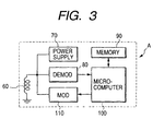
- the IC card “A” includes an antenna 60 , a power supply circuit 70, a demodulation circuit 80. a memory 90, a microcomputer 100, and a modulation circuit 110.
- the antenna 60 is connected to the power supply circuit 70, the demodulation circuit 80, and the modulation circuit 110.
- the microcomputer 100 is connected to the demodulation circuit 80. the memory 90. and the modulation circuit 110.
- a radio signal coming from the reader/writer RW is received by the antenna 60.
- the received radio signal is fed from the antenna 60 to the power supply circuit 70 and the demodulation circuit 80.
- the power supply circuit 70 generates DC power from the received radio signal, and stores the generated DC power.
- the power supply circuit 70 feeds the DC power to the demodulation circuit 80, the memory 90, the microcomputer 100, and the modulation circuit 110 to activate them.
- the demodulation circuit 80 subjects the received radio signal to demodulation, thereby recovering baseband data therefrom.
- the demodulation circuit 80 outputs the recovered data to the microcomputer 100.
- the memory 90 is previously loaded with data representing an anti-collision technique used by the related IC card (the IC card "A"), data representing an identification code word corresponding to a type of the related IC card (the IC card “A”), and data representing parameters of the related IC card (the IC card “A”).
- the memory 90 can be accessed by the microcomputer 100.
- the anti-collision technique used by the IC card “A” is of, for example. the slotted ALOHA type.
- the microcomputer 100 includes a combination of an input/output port, a CPU, a ROM, and a RAM.
- the microcomputer 100 operates in accordance with a program stored in the ROM.
- the program has a first segment for implementing radio communications with the reader/writer RW.
- the program has a second segment designed to process requirements for the transmission of the information of the anti-collision technique used by the related IC card (the IC card "A”) and the identification information of the type of the related IC card (the IC card "A").
- the modulation circuit 110 receives output data (a baseband signal) from the microcomputer 100.
- the modulation circuit 110 subjects the output data from the microcomputer 100 to modulation, thereby converting the data (the baseband signal) into a radio signal.
- the modulation circuit 110 outputs the radio signal to the antenna 60.
- the radio signal is radiated by the antenna 60.
- an anti-collision technique used by the IC card “B” is the same as that used by the IC card “A”, and that anti-collision techniques used by the respective IC cards “C” and “D” are different from each other and are also different from that used by the IC cards “A” and “B”.
- the anti-collision technique used by the IC cards “A” and “B” is referred to as the first anti-collision technique.
- the anti-collision technique used by the IC card “C” is referred to as the second anti-collision technique.
- the anti-collision technique used by the IC card “D” is referred to as the third anti-collision technique.
- the anti-collision technique data in the memory 90 of the IC card “B” is the same as that in the memory 90 of the IC card “A”.
- the anti-collision technique data in the memory 90 of the IC card “C” and the anti-collision technique data in the memory 90 of the IC card “D” are different from each other, and are also different from that in the memory 90 of the IC card "A” or the IC card "B”.
- the program in the microcomputer 100 of the IC card “B” is similar to that in the microcomputer 100 of the IC card “A”.
- the program in the microcomputer 100 of the IC card “C” or “D” is basically similar to that in the microcomputer 100 of the IC card “A” except a portion related to the used anti-collision technique.
- the contactless IC card communication system operates as follows. It is assumed that as shown in Fig. 1, the IC cards "A”, “B”, “C”, and “D” exist in the communication service area provided by the reader/writer RW.
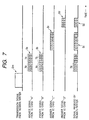
- the microcomputer 10 outputs a signal Srw (see Fig. 6) of a requirement for the identification of IC-card anti-collision techniques to the modulation circuit 30.
- the modulation circuit 30 converts the anti-collision technique identification requirement signal Srw into a corresponding command radio signal referred to as a first command radio signal.
- the modulation circuit 30 outputs the first command radio signal to the antenna 40.
- the first command radio signal is radiated by the antenna 40, being transmitted from the reader/writer RW to the IC cards "A", "B", “C”, and "D".
- the first command radio signal is received by the antenna 60.
- the received first command radio signal is fed from the antenna 60 to the demodulation circuit 80.
- the demodulation circuit 80 recovers the anti-collision technique identification requirement signal Srw from the received first command radio signal.
- the demodulation circuit 80 outputs the recovered anti-collision technique identification requirement signal Srw to the microcomputer 100.
- the microcomputer 100 reads out the data from the memory 90 in response to the anti-collision technique identification requirement signal Srw, and generates an answer signal Sa, Sb, Sc, or Sd (see Fig. 6) from the readout data.
- the microcomputer 100 outputs the answer signal Sa, Sb, Sc, or Sd (see Fig. 6) to the modulation circuit 110.
- the answer signal Sa, Sb, Sc, or Sd contains the information of the anti-collision technique used by the related IC card.
- the answer signal Sa outputted from the microcomputer 100 in the IC card “A” includes 8-bit serial-form data divided into 4-bit serial-form data Xa representing the anti-collision technique used by the IC card “A” (the first anti-collision technique), and 4-bit serial-form data Ya representing parameters of the IC card “A” (see Fig. 7).
- the answer signal Sb outputted from the microcomputer 100 in the IC card “B” includes 8-bit serial-form data divided into 4-bit serial-form data Xa representing the anti-collision technique used by the IC card “B” (the first anti-collision technique), and 4-bit serial-form data Yb representing parameters of the IC card “B” (see Fig. 7).
- the former 4-bit portions of the 8-bit answer signals Sa and Sb are the same as shown in Fig. 7 since the first anti-collision technique is used in common by the IC cards "A" and "B".
- the answer signal Sc outputted from the microcomputer 100 in the IC card “C” includes 8-bit serial-form data representing the anti-collision technique used by the IC card “C” (see Fig. 7), that is, representing the second anti-collision technique.
- the answer signal Sd outputted from the microcomputer 100 in the IC card “D” includes 4-bit serial-form data representing the anti-collision technique used by the IC card “D” (see Fig. 7), that is, the third anti-collision technique.
- the time of the outputting of each of the answer signals Sa and Sb from the related microcomputer 100 is in a given time interval T1.
- the time interval T1 starts from the moment at which the recovered anti-collision technique identification requirement signal Srw is inputted into the microcomputer 100 from the demodulation circuit 80.
- the time of the outputting of the answer signal Sc from the related microcomputer 100 is in a given time interval T2 immediately following the time interval T1.
- the time of the outputting of the answer signal Sd from the related microcomputer 100 is in a given time interval T3 immediately following the time interval T2. This timing difference is provided by the differences among the first, second, and third anti-collision techniques.
- the modulation circuit 110 converts the anti-collision technique answer signal Sa into a corresponding radio answer signal Ra.
- the modulation circuit 110 feeds the radio answer signal Ra to the antenna 60.
- the antenna 60 radiates and transmits the radio answer signal Ra.
- the modulation circuit 110 converts the anti-collision technique answer signal Sb into a corresponding radio answer signal Rb.
- the modulation circuit 110 feeds the radio answer signal Rb to the antenna 60.
- the antenna 60 radiates and transmits the radio answer signal Rb.
- the modulation circuit 110 converts the anti-collision technique answer signal Sc into a corresponding radio answer signal Rc.
- the modulation circuit 110 feeds the radio answer signal Rc to the antenna 60.
- the antenna 60 radiates and transmits the radio answer signal Rc.
- the modulation circuit 110 converts the anti-collision technique answer signal Sd into a corresponding radio answer signal Rd.
- the modulation circuit 110 feeds the radio answer signal Rd to the antenna 60.
- the antenna 60 radiates and transmits the radio answer signal Rd.
- the antenna 40 in the reader/writer RW receives the radio answer signals Ra and Rb from the antennas 60 of the IC cards "A" and “B” at substantially the same timing. Then, the antenna 40 receives the radio answer signal Rc from the antenna 60 of the IC card “C”. Subsequently, the antenna 40 receives the radio answer signal Rd from the antenna 60 of the IC card "D”.
- the received radio answer signals Ra and Rb are fed from the antenna 40 to the demodulation circuit 50. Then, the received radio answer signal Rc is fed from the antenna 40 the demodulation circuit 50. Subsequently, the received radio answer signal Rd is fed from the antenna 40 to the demodulation circuit 50.
- the demodulation circuit 50 accurately recovers at least former halves of the anti-collision technique answer signals Sa and Sb from the received radio answer signals Ra and Rb even if latter halves thereof fail to be accurately detected.
- the demodulation circuit 50 outputs the recovered anti-collision technique answer signals Sa and Sb to the microcomputer 10. Then, the demodulation circuit 50 recovers the anti-collision technique answer signal Sc from the received radio answer signal Rc.
- the demodulation circuit 50 outputs the recovered anti-collision technique answer signal Sc to the microcomputer 10. Subsequently, the demodulation circuit 50 recovers the anti-collision technique answer signal Sd from the received radio answer signal Rd.
- the demodulation circuit 50 outputs the recovered anti-collision technique answer signal Sd to the microcomputer 10.
- the microcomputer 10 decides that at least one answer to the anti-collision technique identification requirement has come from an IC card using the first anti-collision technique, and that at least one IC card using the first anti-collision technique is present in the communication service area.
- the microcomputer 10 decides that at least one answer to the anti-collision technique identification requirement has come from an IC card using the second anti-collision technique, and that at least one IC card using the second anti-collision technique is present in the communication service area.
- the microcomputer 10 decides that at least one answer to the anti-collision technique identification requirement has come from an IC card using the third anti-collision technique, and that at least one IC card using the third anti-collision technique is present in the communication service area.
- the microcomputer 10 implements steps of identifying the types of the IC cards "A", “B", “C”, and “D” in dependence upon the anti-collision techniques. Specifically, in response to the first anti-collision technique represented by the answer signal Sa or Sb the microcomputer 10 accesses the data in the memory 20 which represents the relation of the first anti-collision technique with a requirement signal. In response to the accessed data, the microcomputer 10 generates a signal Sc ⁇ of a requirement for the identification of the type of the IC card (the types of the IC cards) using the first anti-collision technique. The microcomputer 10 outputs the card type identification requirement signal Sc ⁇ to the modulation circuit 30 (see Fig. 6).
- the card type identification requirement signal Sc ⁇ has a card type identification requirement code word corresponding to the first anti-collision technique (the anti-collision technique used by the IC cards "A” and "B").
- the time of the outputting of the card type identification requirement signal Sc ⁇ from the microcomputer 10 is in a given time interval T4.
- the time interval T4 starts from the moment at which the microcomputer 10 decides that an answer to the anti-collision technique identification requirement has come from the IC card using the first anti-collision technique (the IC card "A” or "B”).
- the microcomputer 10 determines the time at which the card type identification requirement signal Sc ⁇ should be outputted in accordance with the first anti-collision technique.
- the modulation circuit 30 converts the card type identification requirement signal Sc ⁇ into a corresponding command radio signal referred to as a second command radio signal.
- the modulation circuit 30 outputs the second command radio signal to the antenna 40.
- the second command radio signal is radiated by the antenna 40, being transmitted from the reader/writer RW.
- the second command radio signal is received by the antenna 60.
- the received second command radio signal is fed from the antenna 60 to the demodulation circuit 80.
- the demodulation circuit 80 recovers the card type identification requirement signal Sc ⁇ from the received second command radio signal.
- the demodulation circuit 80 outputs the recovered card type identification requirement signal Sc ⁇ to the microcomputer 100.
- the microcomputer 100 reads out the data from the memory 90 in response to the card type identification requirement signal Sc ⁇ , and generates an answer signal Sca (see Fig. 6) from the readout data.
- the microcomputer 100 outputs the generated answer signal Sca to the modulation circuit 110.
- the answer signal Sca contains the identification information of the type of the IC card “A” which is related to the anti-collision technique (the first anti-collision technique) used by the IC card "A".
- the time of the outputting of the card type identification answer signal Sca is in the time interval T4 (see Fig. 6).
- the modulation circuit 110 converts the card type identification answer signal Sca into a corresponding radio answer signal Raa.
- the modulation circuit 110 feeds the radio answer signal Raa to the antenna 60.
- the antenna 60 radiates and transmits the radio answer signal Raa.
- the antenna 40 in the reader/writer RW receives the radio answer signal Raa from the antenna 60 of the IC card "A".
- the received radio answer signal Raa is fed from the antenna 40 to the demodulation circuit 50.
- the demodulation circuit 50 recovers the card type identification answer signal Sca from the received radio answer signal Raa.
- the demodulation circuit 50 outputs the recovered card type identification answer signal Sca to the microcomputer 10.
- the microcomputer 10 generates a card type identification code word, which corresponds to the IC card "A", in response to the card type identification answer signal Sca.
- the microcomputer 10 writes data of the generated card type identification code word in the memory 20.
- the data of the generated card type identification word in the memory 20 will be used later in IC card control.
- the IC card “B” receives the second command radio signal from the reader/writer RW, and recovers the card type identification requirement signal Sc ⁇ from the received second command radio signal as the IC card "A” does.
- the microcomputer 100 reads out the data from the memory 90 in response to the card type identification requirement signal Sc ⁇ , and generates an answer signal Scb (see Fig. 6) from the readout data.
- the microcomputer 100 outputs the answer signal Scb to the modulation circuit 110.
- the answer signal Scb contains the information of the type of the IC card "B” which is related to the anti-collision technique (the first anti-collision technique) used by the IC card "B".
- the time of the outputting of the card type identification answer signal Scb is in the time interval T4 (see Fig. 6).
- the time of the outputting of the card type identification answer signal Scb follows the time of the outputting of the card type identification signal Sca.
- This timing difference is provided by the anti-collision technique used by the IC cards "A" and "B".
- the modulation circuit 110 converts the card type identification answer signal Scb into a corresponding radio answer signal Rab.
- the IC card “B” transmits the radio answer signal Rab to the reader/writer RW.
- the reader/writer RW identifies the type of the IC card "B” in response to the radio answer signal Rab similarly to the identification of the type of the IC card "A".
- the reader/writer RW sequentially implements the identification of the type of the IC card “C” and the identification of the type of the IC card “D”.
- the microcomputer 10 in the reader/writer RW accesses the data in the memory 20 which represents the relation of the second anti-collision technique with a requirement signal.
- the microcomputer 10 In response to the accessed data, the microcomputer 10 generates a signal Sc ⁇ of a requirement for the identification of the type of the IC card using the second anti-collision technique.
- the microcomputer 10 outputs the card type identification requirement signal Sc ⁇ to the modulation circuit 30 (see Fig. 6).
- the card type identification requirement signal Sc ⁇ has a card type identification code word corresponding to the IC card using the second anti-collision technique (the anti-collision technique used by the IC card "C"). As shown in Fig.
- the time of the outputting of the card type identification requirement signal Sc ⁇ from the microcomputer 10 is in an initial part of a given time interval T5 following the time interval T4.
- the microcomputer 10 determines the time at which the card type identification requirement signal Sc ⁇ should be outputted in accordance with the second anti-collision technique.
- the modulation circuit 30 converts the card type identification requirement signal Sc ⁇ into a corresponding command radio signal referred to as a third command radio signal.
- the modulation circuit 30 outputs the third command radio signal to the antenna 40.
- the third command radio signal is radiated by the antenna 40, being transmitted from the reader/writer RW.
- the third command radio signal is received by the antenna 60.
- the received third command radio signal is fed from the antenna 60 to the demodulation circuit 80.
- the demodulation circuit 80 recovers the card type identification requirement signal Sc ⁇ from the received third command radio signal.
- the demodulation circuit 80 outputs the recovered card type identification requirement signal Sc ⁇ to the microcomputer 100.
- the microcomputer 100 reads out the data from the memory 90 in response to the card type identification requirement signal Sc ⁇ , and generates an answer signal Scc (see Fig. 6) from the readout data.
- the microcomputer 100 outputs the generated answer signal Scc to the modulation circuit 110.
- the answer signal Scc contains the identification information of the type of the IC card “C” which is related to the anti-collision technique (the second anti-collision technique) used by the IC card “C”.
- the time of the outputting of the card type identification answer signal Scc is in the time interval T5 (see Fig. 6).
- the modulation circuit 110 converts the card type identification answer signal Scc into a corresponding radio answer signal Rac.
- the modulation circuit 110 feeds the radio answer signal Rac to the antenna 60.
- the antenna 60 radiates and transmits the radio answer signal Rac.
- the antenna 40 in the reader/writer RW receives the radio answer signal Rac from the antenna 60 of the IC card "C".
- the received radio answer signal Rac is fed from the antenna 40 to the demodulation circuit 50.
- the demodulation circuit 50 recovers the card type identification answer signal Scc from the received radio answer signal Rac.
- the demodulation circuit 50 outputs the recovered card type identification answer signal Scc to the microcomputer 10.
- the microcomputer 10 generates a card type identification code word, which corresponds to the IC card "C”, in response to the card type identification answer signal Scc.
- the microcomputer 10 writes data of the generated card type identification code word in the memory 20.
- the data of the generated card type identification word in the memory 20 will be used later in IC card control.
- the reader/writer RW implements the identification of the type of the IC card "D" as follows.
- the microcomputer 10 in the reader/writer RW accesses the data in the memory 20 which represents the relation of the third anti-collision technique with a requirement signal.
- the microcomputer 10 In response to the accessed data, the microcomputer 10 generates a signal Sc ⁇ of a requirement for the identification of the type of the IC card using the third anti-collision technique.
- the microcomputer 10 outputs the card type identification requirement signal Sc ⁇ to the modulation circuit 30 (see Fig. 6).
- the card type identification requirement signal Sc ⁇ has a card type identification code word corresponding to the IC card using the third anti-collision technique (the anti-collision technique used by the IC card "D"). As shown in Fig.
- the time of the outputting of the card type identification requirement signal Sc ⁇ from the microcomputer 10 is in an initial part of a given time interval T6 following the time interval T5.
- the microcomputer 10 determines the time at which the card type identification requirement signal Scy should be outputted in accordance with the third anti-collision technique.
- the microcomputer 10 outputs the card type identification requirement signals Sc ⁇ , Sc ⁇ , and Sc ⁇ at respective different timings according to the differences among the first, second, and third anti-collision techniques.
- the modulation circuit 30 converts the card type identification requirement signal Sc ⁇ into a corresponding command radio signal referred to as a fourth command radio signal.
- the modulation circuit 30 outputs the fourth command radio signal to the antenna 40.
- the fourth command radio signal is radiated by the antenna 40, being transmitted from the reader/writer RW.
- the fourth command radio signal is received by the antenna 60.
- the received fourth command radio signal is fed from the antenna 60 to the demodulation circuit 80.
- the demodulation circuit 80 recovers the card type identification requirement signal Sc ⁇ from the received fourth command radio signal.
- the demodulation circuit 80 outputs the recovered card type identification requirement signal Sc ⁇ to the microcomputer 100.
- the microcomputer 100 reads out the data from the memory 90 in response to the card type identification requirement signal Scy. and generates an answer signal Sed (see Fig. 6) from the readout data.
- the microcomputer 100 outputs the generated answer signal Scd to the modulation circuit 110.
- the answer signal Scd contains the identification information of the type of the IC card “D” which is related to the anti-collision technique (the third anti-collision technique) used by the IC card "D".
- the time of the outputting of the card type identification answer signal Scd is in the time interval T6 (see Fig. 6).
- the modulation circuit 110 converts the card type identification answer signal Scd into a corresponding radio answer signal Rad.
- the modulation circuit 110 feeds the radio answer signal Rad to the antenna 60.
- the antenna 60 radiates and transmits the radio answer signal Rad.
- the antenna 40 in the reader/writer RW receives the radio answer signal Rad from the antenna 60 of the IC card "D".
- the received radio answer signal Rad is fed from the antenna 40 to the demodulation circuit 50.
- the demodulation circuit 50 recovers the card type identification answer signal Scd from the received radio answer signal Rad.
- the demodulation circuit 50 outputs the recovered card type identification answer signal Scd to the microcomputer 10.
- the microcomputer 10 generates a card type identification code word, which corresponds to the IC card "D", in response to the card type identification answer signal Scd.
- the microcomputer 10 writes data of the generated card type identification code word in the memory 20.
- the data of the generated card type identification word in the memory 20 will be used later in IC card control.
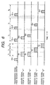
- Fig. 4 is a flowchart of the program in the microcomputer 10.
- a first step 200 of the program outputs an anti-collision technique identification requirement signal Srw to the modulation circuit 30. After the step 200, the program advances to a step 210.
- the step 210 decides whether or not an anti-collision technique answer signal in the first anti-collision technique is present. This decision relates to the anti-collision technique answer signals Sa and Sb transmitted from the IC cards "A" and "B".
- the program advances from the step 210 to a step 220. Otherwise, the program jumps from the step 210 to a step 230.
- the step 210 decides whether or not an anti-collision technique answer signal in the second anti-collision technique is present. This decision relates to the anti-collision technique answer signal Sc transmitted from the IC card "C".
- the program advances from the step 210 to the step 220. Otherwise, the program jumps from the step 210 to the step 230.
- the step 210 decides whether or not an anti-collision technique answer signal in the second anti-collision technique is present. This decision relates to the anti-collision technique answer signal Sd transmitted from the IC card "D".
- the program advances from the step 210 to the step 220. Otherwise, the program jumps from the step 210 to the step 230.
- the step 220 sets a flag related to the anti-collision technique answer signal decided by the step 210.
- the set flag represents the presence of the anti-collision technique answer signal decided by the step 210. In other words, the set flag represents that an IC card using the anti-collision technique represented by the answer signal is present in the communication service area.
- the step 230 decides whether or not the lapse of time from the moment of the outputting of the anti-collision technique identification requirement signal Srw reaches a predetermined time interval "T" which covers the time intervals T1, T2, and T3 (see Fig. 6).
- a predetermined time interval "T” which covers the time intervals T1, T2, and T3 (see Fig. 6).
- the program returns from the step 230 to the step 210.
- the program advances from the step 230 to a step 240.
- the step 240 decides whether or not at least one flag set by the step 220 is present. In other words, the step 240 decides whether or not at least one anti-collision technique answer signal in an anti-collision technique is present.
- the program advances from the step 240 to a subroutine block 250. Otherwise, the program exits from the step 240, and then the current execution cycle of the program ends.
- the subroutine block 250 accesses the data in the memory 20, which represents the relation of the first anti-collision technique (the anti-collision technique used by the IC cards "A” and “B") with a requirement signal, in response to the set flags related to the anti-collision technique answer signals Sa and Sb.
- the subroutine block 250 generates a signal Sc ⁇ of a requirement for the identification of the type of the related IC card or the types of the related IC cards (the types of the IC cards "A” and "B") in response to the accessed data.
- the subroutine block 250 outputs the card type identification requirement signal Sc ⁇ to the modulation circuit 30.
- the card type identification requirement signal Sc ⁇ has a card type identification requirement code word corresponding to the first anti-collision technique (the anti-collision technique used by the IC cards "A” and “B"). Then, the microcomputer 10 receives the card type identification answer signal Sca from the IC card "A”. The subroutine block 250 generates a card type identification code word, which corresponds to the IC card "A”, in response to the card type identification answer signal Sca. The subroutine block 250 writes data of the generated card type identification code word in the memory 20. The subroutine block 250 resets the flag related to the anti-collision technique answer signals Sa. Then, the microcomputer 10 receives the card type identification answer signal Scb from the IC card "B".
- the subroutine block 250 generates a card type identification code word, which corresponds to the IC card "B", in response to the card type identification answer signal Scb.
- the subroutine block 250 writes data of the generated card type identification code word in the memory 20.
- the subroutine block 250 resets the flag related to the anti-collision technique answer signals Sb. Then, the program advances from the subroutine block 250 to a step 260.
- the step 260 decides whether or not at least one IC card to be identified remains by referring to, for example, the flags related to the anti-collision technique answer signals Sa, Sb. Sc, and Sd.
- the program returns from the step 260 to the subroutine block 250. Otherwise, the program exits from the step 260, and then the current execution cycle of the program ends.
- the subroutine block 250 accesses the data in the memory 20, which represents the relation of the second anti-collision technique (the anti-collision technique used by the IC card "C") with a requirement signal, in response to the set flag related to the anti-collision technique answer signal Sc.
- the subroutine block 250 generates a signal Sc ⁇ of a requirement for the identification of the type of the related IC card (the IC card "C") in response to the accessed data.
- the subroutine block 250 outputs the card type identification requirement signal Sc ⁇ to the modulation circuit 30.
- the card type identification requirement signal Sc ⁇ has a card type identification requirement code word corresponding to the second anti-collision technique (the anti-collision technique used by the IC card "C").
- the microcomputer 10 receives the card type identification answer signal Scc from the IC card "C".
- the subroutine block 250 generates a card type identification code word, which corresponds to the IC card "C", in response to the card type identification answer signal Scc.
- the subroutine block 250 writes data of the generated card type identification code word in the memory 20.
- the subroutine block 250 resets the flag related to the anti-collision technique answer signals Sc. Then, the program advances from the subroutine block 250 to the step 260.
- the step 260 decides whether or not at least one IC card to be identified remains by referring to, for example, the flags related to the anti-collision technique answer signals Sa, Sb, Sc, and Sd.
- the program returns from the step 260 to the subroutine block 250. Otherwise, the program exits from the step 260, and then the current execution cycle of the program ends.
- the subroutine block 250 accesses the data in the memory 20, which represents the relation of the third anti-collision technique (the anti-collision technique used by the IC card "D") with a requirement signal, in response to the set flag related to the anti-collision technique answer signal Sd.
- the subroutine block 250 generates a signal Sc ⁇ of a requirement for the identification of the type of the related IC card (the IC card "D") in response to the accessed data.
- the subroutine block 250 outputs the card type identification requirement signal Scy to the modulation circuit 30.
- the card type identification requirement signal Sc ⁇ has a card type identification requirement code word corresponding to the third anti-collision technique (the anti-collision technique used by the IC card "D").
- the microcomputer 10 receives the card type identification answer signal Scd from the IC card "D".
- the subroutine block 250 generates a card type identification code word, which corresponds to the IC card "D", in response to the card type identification answer signal Scd.
- the subroutine block 250 writes data of the generated card type identification code word in the memory 20.
- the subroutine block 250 resets the flag related to the anti-collision technique answer signals Sd.
- the program advances to the step 260.
- the step 260 decides whether or not at least one IC card to be identified remains by referring to. for example. the flags related to the anti-collision technique answer signals Sa, Sb, Sc. and Sd. When any IC card to be identified does not remain, the program exits from the step 260 and then the current execution cycle of the program ends.
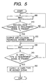
- Fig. 5 is a flowchart of the program in the microcomputer 100.
- a first step 300 of the program waits a given short time interval. Then, the program advances from the step 300 to a step 310.
- the step 310 decides whether or not an anti-collision technique identification requirement signal Srw is present.
- an anti-collision technique identification requirement signal Srw is present, the program advances from the step 310 to a step 320. Otherwise, the program returns from the step 310 to the step 300.
- the step 320 reads out the data from the memory 90, and generates an answer signal Sa from the readout data.
- the step 320 determines a desired output timing on the basis of the readout data.
- the desired output timing depends on the anti-collision technique used by the present IC card (the IC card "A").
- the step 320 outputs the generated answer signal Sa to the modulation circuit 110 at a timing equal to the desired output timing.
- the answer signal Sa contains the information of the anti-collision technique used by the IC card "A" (that is, the first anti-collision technique).
- the step 330 waits a given short time interval. Then, the program advances from the step 330 to a step 340.
- the step 340 decides whether or not a card type identification requirement signal Sc ⁇ is present. When a card type identification requirement signal Sc ⁇ is present, the program advances from the step 340 to a step 350. Otherwise, the program returns from the step 340 to the step 330.
- the step 350 reads out the data from the memory 90 in response to the card type identification requirement signal Sc ⁇ , and generates an answer signal Sca from the readout data.
- the step 350 determines a desired output timing on the basis of the readout data.
- the desired output timing depends on the identification information of the present IC card (the IC card "A").
- the step 350 outputs the generated answer signal Sca to the modulation circuit 110 at a timing equal to the desired output timing.
- the answer signal Sca contains the identification information of the type of the IC card "A" which is related to the anti-collision technique used by the related IC card "A" (that is, the first anti-collision technique).
- the telephone set on which the reader/writer RW is provided may be replaced by a dispenser or an automatic vending machine.
- microcomputers 10 and 100 may be replaced by exclusive control circuits composed of discrete analog circuits or discrete digital circuits.
- At least part of the combination of the microcomputer 10, the memory 20, the modulation circuit 30, and the demodulation circuit 50 may be formed by a single IC chip.
- At least part of the combination of the memory 90, the microcomputer 100 the power supply circuit 70, the modulation circuit 110, and the demodulation circuit 80 may be formed by a single IC chip.
Landscapes
- Engineering & Computer Science (AREA)
- Physics & Mathematics (AREA)
- Health & Medical Sciences (AREA)
- Toxicology (AREA)
- General Physics & Mathematics (AREA)
- Artificial Intelligence (AREA)
- Computer Vision & Pattern Recognition (AREA)
- Theoretical Computer Science (AREA)
- Electromagnetism (AREA)
- General Health & Medical Sciences (AREA)
- Computer Networks & Wireless Communication (AREA)
- Computer Security & Cryptography (AREA)
- Radar Systems Or Details Thereof (AREA)
- Credit Cards Or The Like (AREA)
- Near-Field Transmission Systems (AREA)
Claims (4)
- Système de communication à cartes à puce sans contact comprenant :caractérisé parun dispositif de lecture/dispositif d'écriture (RW) et des cartes à puce (A à D) qui communiquent les uns avec les autres sur une base sans contact en conformité avec des techniques d'anti-collision ;
des premiers moyens (200, 20, 30, 40) disposés dans le dispositif de lecture/dispositif d'écriture (RW) pour implémenter une demande d'identification par rapport à des techniques d'anti-collision données parmi les techniques d'anti-collision ;
des seconds moyens (320, 90, 60, 110) disposés dans les cartes à puce respectives parmi les cartes à puce (A à D) qui utilisent différentes techniques d'anti-collision respectivement pour implémenter des réponses à la demande d'identification des techniques d'anti-collision par les premiers moyens (200, 20, 30, 40) à des cadencements différents en fonction des différentes techniques d'anti-collision respectivement ;
des troisièmes moyens (250, 20, 30, 40) disposés dans le dispositif de lecture/dispositif d'écriture (RW) pour demander, en fonction des techniques d'anti-collision données, des identifications des types de cartes à puce (A à D) en réponse aux réponses par les seconds moyens (320, 90, 60, 110) ;
des quatrièmes moyens (350, 60, 90, 110) disposés dans les cartes à puce respectives parmi les cartes à puce (A à D) qui utilisent différentes techniques d'anti-collision respectivement pour retourner des données d'identification des cartes à puce concernées en réponse aux demandes d'identification du type de cartes par les troisièmes moyens (250, 20, 30, 40) ; et
des cinquièmes moyens (250,' 20, 30, 40) disposés dans le dispositif de lecture/dispositif d'écriture (RW) pour identifier les types de cartes à puce (A à D) en réponse aux données d'identification retournées par les quatrièmes moyens (350, 60, 90, 110). - Procédé de communication à cartes à puce sans contact dans lequel un dispositif de lecture/dispositif d'écriture (RW) et des cartes à puce (A à D) communiquent les uns avec les autres sur une base sans contact en conformité avec des techniques d'anti-collision, le procédé étant caractérisé en ce qu'il comprend les étapes consistant à :amener le dispositif de lecture/dispositif d'écriture (RW) à implémenter une demande d'identification par rapport à des techniques d'anti-collision données parmi les techniques d'anti-collision par le dispositif de lecture/dispositif d'écriture (RW) ;implémenter des réponses à la demande d'identification des techniques d'anti-collision par le dispositif de lecture/dispositif d'écriture (RW) pour des cartes à puce respectives parmi les cartes à puce (A à D) qui utilisent différentes techniques d'anti-collision respectivement à des cadencements différents en fonction des différentes techniques d'anti-collision respectivement ;amener le dispositif de lecture/dispositif d'écriture (RW) à demander des identifications des types de cartes à puce (A à D) en fonction des techniques d'anti-collision données en réponse aux réponses pour les cartes à puce respectives ;retourner des données d'identification des cartes à puce (A à D) en réponse aux demandes d'identification du type de cartes par le dispositif de lecture/dispositif d'écriture (RW) pour les cartes à puce respectives parmi les cartes à puce (A à D) qui utilisent différentes techniques d'anti-collision respectivement ; etamener le dispositif de lecture/dispositif d'écriture (RW) à identifier les types de cartes à puce (A à D) en réponse aux données d'identification des cartes à puce respectives (A à D).
- Système de communication à cartes à puce sans contact selon la revendication 1, dans lequel
une première carte à puces desdites cartes à puce (A à D) utilise une première technique d'anti-collision ;
une seconde carte à puce desdites cartes à puce (A à D) utilise une seconde technique d'anti-collision différente de la première technique d'anti-collision ;
lesdits premiers moyens (200, 20, 30, 40) servent à transmettre un premier signal de demande à la première carte à puce et à la seconde carte à puce ;
lesdits seconds moyens (320, 90, 60, 110) disposés dans la première carte à puce servent à générer un premier signal de réponse en réponse au premier signal de demande transmis depuis le dispositif de lecture/dispositif d'écriture (RW) et pour retourner le premier signal de réponse au dispositif de lecture/dispositif d'écriture (RW) à un premier cadencement en fonction de la technique d'anti-collision utilisée par la première carte à puce, le premier signal de réponse représentant la technique d'anti-collision utilisée par la première carte à puce ;
lesdits seconds moyens (320, 90, 60, 110) disposés dans la seconde carte à puce servent à générer un second signal de réponse en réponse au premier signal de demande transmis depuis le dispositif de lecture/dispositif d'écriture (RW) et pour retourner le second signal de réponse au dispositif de lecture/dispositif d'écriture (RW) à un second cadencement en fonction de la technique d'anti-collision utilisée par la seconde carte à puce différent du premier cadencement, le second signal de réponse représentant la technique d'anti-collision utilisée par la seconde carte à puce ;
lesdits troisièmes moyens (250, 20, 30, 40) servent à générer un second signal de demande en réponse au premier signal de réponse transmis depuis la première carte à puce et pour transmettre le second signal de demande à la première carte à puce à un troisième cadencement déterminé par la technique d'anti-collision représentée par le premier signal de réponse ; et
lesdits troisièmes moyens (250, 20, 30, 40) servent à générer un troisième signal de demande en réponse au second signal de réponse transmis depuis la seconde carte à puce et pour transmettre le troisième signal de demande à la seconde carte à puce à un quatrième cadencement différent du troisième cadencement déterminé par la technique d'anti-collision représentée par le second signal de réponse. - Système de communication à cartes à puce sans contact selon la revendication 3, dans lequel :lesdits quatrièmes moyens (350, 60, 90, 110) disposés dans la première carte à puce servent à générer un troisième signal de réponse et à retourner le troisième signal de réponse au dispositif de lecture/dispositif d'écriture (RW) en réponse au second signal de demande transmis depuis le dispositif de lecture/dispositif d'écriture (RW), le troisième signal de réponse représentant les informations d'identification de la première carte à puce ;lesdits quatrièmes moyens (350, 60, 90, 110) disposés dans la seconde carte à puce servent à générer un quatrième signal de réponse et à retourner le quatrième signal de réponse au dispositif de lecture/dispositif d'écriture (RW) en réponse au troisième signal de demande transmis depuis le dispositif de lecture/dispositif d'écriture (RW), le quatrième signal de réponse représentant les informations d'identification de la seconde carte à puce ;lesdits cinquièmes moyens (250, 20, 30, 40) sont destinés à récupérer les informations d'identification de la première carte à puce à partir du troisième signal de réponse transmis depuis celle-ci et pour mémoriser les informations d'identification récupérées de la première carte à puce ; etlesdits cinquièmes moyens (250, 20, 30, 40) sont destinés à récupérer les informations d'identification de la seconde carte à puce à partir du quatrième signal de réponse transmis depuis celle-ci et pour mémoriser les informations d'identification récupérées de la seconde carte à puce.
Applications Claiming Priority (2)
| Application Number | Priority Date | Filing Date | Title |
|---|---|---|---|
| JP423398A JP3239294B2 (ja) | 1998-01-12 | 1998-01-12 | 非接触式icカード通信システム及びicカード通信方法 |
| JP423398 | 1998-01-12 |
Publications (3)
| Publication Number | Publication Date |
|---|---|
| EP0929048A2 EP0929048A2 (fr) | 1999-07-14 |
| EP0929048A3 EP0929048A3 (fr) | 2000-03-01 |
| EP0929048B1 true EP0929048B1 (fr) | 2004-11-17 |
Family
ID=11578853
Family Applications (1)
| Application Number | Title | Priority Date | Filing Date |
|---|---|---|---|
| EP99100093A Expired - Lifetime EP0929048B1 (fr) | 1998-01-12 | 1999-01-05 | Système et méthode de communication sans fil avec carte à puce |
Country Status (4)
| Country | Link |
|---|---|
| US (1) | US6388562B1 (fr) |
| EP (1) | EP0929048B1 (fr) |
| JP (1) | JP3239294B2 (fr) |
| DE (1) | DE69921866T2 (fr) |
Families Citing this family (15)
| Publication number | Priority date | Publication date | Assignee | Title |
|---|---|---|---|---|
| JP2001136100A (ja) * | 1999-11-04 | 2001-05-18 | Matsushita Electronics Industry Corp | 情報通信処理方式 |
| JP2001167241A (ja) * | 1999-12-10 | 2001-06-22 | Fujitsu Ltd | 非接触icカード及びその製造方法 |
| MXPA02011493A (es) | 2001-11-28 | 2005-02-17 | Seiko Epson Corp | Comunicacion sin contacto entre el dispositivo y el cartucho que contiene componente consumible. |
| DE10349647B4 (de) * | 2003-10-21 | 2006-08-10 | Atmel Germany Gmbh | Verfahren zur Auswahl eines oder mehrerer Transponder |
| JP4692807B2 (ja) | 2004-12-21 | 2011-06-01 | ソニー株式会社 | 接触式データ通信装置、送受信装置、および送受信方法 |
| KR101059872B1 (ko) * | 2005-01-03 | 2011-08-29 | 삼성전자주식회사 | 고유 식별자를 이용한 통신충돌방지 프로토콜 |
| JP4305854B2 (ja) * | 2005-01-19 | 2009-07-29 | 富士フイルム株式会社 | 画像管理装置及び方法 |
| US7274284B2 (en) * | 2005-02-04 | 2007-09-25 | Atmel Corporation | Method for RF card detection in a contactless system |
| JP5027398B2 (ja) | 2005-09-27 | 2012-09-19 | ルネサスエレクトロニクス株式会社 | Icタグ識別方法 |
| JP2007114821A (ja) * | 2005-10-18 | 2007-05-10 | Hitachi Ltd | Rfidタグ、rfidリーダ・ライタ、rfidシステムおよびrfidシステムの処理方法 |
| US20070297214A1 (en) * | 2006-06-09 | 2007-12-27 | Semiconductor Energy Laboratory Co., Ltd. | Semiconductor device |
| CN102656813B (zh) | 2009-12-17 | 2015-07-01 | 阿尔卡特朗讯 | 使用带宽自适应预编码器接口的串扰控制方法和装置 |
| US9323964B2 (en) * | 2013-08-20 | 2016-04-26 | Cubic Corporation | Card detection and selection |
| CN107403119B (zh) * | 2017-06-13 | 2021-04-23 | 北京三快在线科技有限公司 | 一种智能卡信息读取方法及装置 |
| EP3493097B1 (fr) * | 2017-11-29 | 2021-03-24 | ams AG | Procédé permettant de fournir de l'énergie sans fil au moyen d'une identification de fréquence radio, rfid et système rfid |
Family Cites Families (6)
| Publication number | Priority date | Publication date | Assignee | Title |
|---|---|---|---|---|
| US4638313A (en) * | 1984-11-08 | 1987-01-20 | Spacelabs, Inc. | Addressing for a multipoint communication system for patient monitoring |
| GB2283600B (en) * | 1993-11-02 | 1997-10-22 | Nippon Denso Co | Communication system |
| JPH08123919A (ja) * | 1994-10-28 | 1996-05-17 | Mitsubishi Electric Corp | 非接触icカードシステムおよびその通信方法 |
| JPH08315090A (ja) * | 1995-05-23 | 1996-11-29 | Toshiba Corp | Icカードリーダライタおよびデータ伝送方法 |
| US5940006A (en) * | 1995-12-12 | 1999-08-17 | Lucent Technologies Inc. | Enhanced uplink modulated backscatter system |
| US5856788A (en) * | 1996-03-12 | 1999-01-05 | Single Chips Systems Corp. | Method and apparatus for radiofrequency identification tags |
-
1998
- 1998-01-12 JP JP423398A patent/JP3239294B2/ja not_active Expired - Lifetime
-
1999
- 1999-01-05 EP EP99100093A patent/EP0929048B1/fr not_active Expired - Lifetime
- 1999-01-05 DE DE69921866T patent/DE69921866T2/de not_active Expired - Lifetime
- 1999-01-12 US US09/228,413 patent/US6388562B1/en not_active Expired - Fee Related
Also Published As
| Publication number | Publication date |
|---|---|
| EP0929048A3 (fr) | 2000-03-01 |
| EP0929048A2 (fr) | 1999-07-14 |
| JPH11203428A (ja) | 1999-07-30 |
| DE69921866T2 (de) | 2005-10-20 |
| DE69921866D1 (de) | 2004-12-23 |
| JP3239294B2 (ja) | 2001-12-17 |
| US6388562B1 (en) | 2002-05-14 |
Similar Documents
| Publication | Publication Date | Title |
|---|---|---|
| EP0929048B1 (fr) | Système et méthode de communication sans fil avec carte à puce | |
| KR100277448B1 (ko) | 비접촉 ic 카드 인식 시스템 및 인식 방법 | |
| US6456191B1 (en) | Tag system with anti-collision features | |
| US7230943B2 (en) | Wireless information processing system with wireless information recording medium and wireless information processing apparatus, and communication method therefor | |
| US8207856B2 (en) | Systems and methods for RFID tag arbitration where RFID tags generate multiple random numbers for different arbitration sessions | |
| US6352202B2 (en) | Method and system for controlling contactless IC cards | |
| US20080136599A1 (en) | Reader/writer apparatus, data access system, data access control method, and computer product | |
| US20080122581A1 (en) | Passive rfid reader and operation control method therefor | |
| US6411200B1 (en) | Card reader/writer and communication method of card reader writer | |
| CN101647028B (zh) | 在自动化组件和移动操作终端之间建立无线通信连接的方法 | |
| EP1780655A1 (fr) | Etiquette RFID, lecteur/enregistreur RFID et méthode de communication | |
| US20120126952A1 (en) | Communication Method in RFID or Remote Sensor Systems | |
| US8457024B2 (en) | Information processing device and program | |
| JP4284745B2 (ja) | Icカード通信システム | |
| CN100437622C (zh) | 激活对等通信单元的通信模式的方法 | |
| US7307964B2 (en) | Contactless communication system and data carrier used for the same | |
| JP2000069028A (ja) | 無線カードとリーダ/ライタと上位装置と無線カードシステムと無線通信機能を有する情報記憶媒体と送受信回路と無線通信システム | |
| JP4116273B2 (ja) | 乱数発生装置を有する無線カード、この無線カード用の半導体装置、およびこの無線カードを用いた無線カードシステム | |
| JP3553763B2 (ja) | Icカードの識別方法 | |
| JPH11167610A (ja) | Icカードシステム及びその通信方法 | |
| EP1502230B1 (fr) | Procede servant a inventorier une pluralite de porteuses de donnees | |
| JP2002366906A (ja) | 携帯可能情報処理装置の非接触通信方法 | |
| JP2000148931A (ja) | カ―ド識別方法の改良 | |
| JP3584332B2 (ja) | 非接触識別システム | |
| JPH08315097A (ja) | 情報媒体および情報媒体処理装置 |
Legal Events
| Date | Code | Title | Description |
|---|---|---|---|
| PUAI | Public reference made under article 153(3) epc to a published international application that has entered the european phase |
Free format text: ORIGINAL CODE: 0009012 |
|
| AK | Designated contracting states |
Kind code of ref document: A2 Designated state(s): DE FR GB |
|
| AX | Request for extension of the european patent |
Free format text: AL;LT;LV;MK;RO;SI |
|
| PUAL | Search report despatched |
Free format text: ORIGINAL CODE: 0009013 |
|
| AK | Designated contracting states |
Kind code of ref document: A3 Designated state(s): AT BE CH CY DE DK ES FI FR GB GR IE IT LI LU MC NL PT SE |
|
| AX | Request for extension of the european patent |
Free format text: AL;LT;LV;MK;RO;SI |
|
| 17P | Request for examination filed |
Effective date: 20000828 |
|
| AKX | Designation fees paid |
Free format text: DE FR GB |
|
| RAP1 | Party data changed (applicant data changed or rights of an application transferred) |
Owner name: NEC TOKIN CORPORATION Owner name: HITACHI, LTD. Owner name: NIPPON TELEGRAPH AND TELEPHONE CORPORATION Owner name: DENSO CORPORATION |
|
| RAP1 | Party data changed (applicant data changed or rights of an application transferred) |
Owner name: NEC TOKIN CORPORATION Owner name: HITACHI, LTD. Owner name: NIPPON TELEGRAPH AND TELEPHONE CORPORATION Owner name: DENSO WAVE INCORPORATED |
|
| 17Q | First examination report despatched |
Effective date: 20030820 |
|
| GRAP | Despatch of communication of intention to grant a patent |
Free format text: ORIGINAL CODE: EPIDOSNIGR1 |
|
| GRAS | Grant fee paid |
Free format text: ORIGINAL CODE: EPIDOSNIGR3 |
|
| GRAA | (expected) grant |
Free format text: ORIGINAL CODE: 0009210 |
|
| AK | Designated contracting states |
Kind code of ref document: B1 Designated state(s): DE FR GB |
|
| REG | Reference to a national code |
Ref country code: GB Ref legal event code: FG4D |
|
| REF | Corresponds to: |
Ref document number: 69921866 Country of ref document: DE Date of ref document: 20041223 Kind code of ref document: P |
|
| ET | Fr: translation filed | ||
| PLBE | No opposition filed within time limit |
Free format text: ORIGINAL CODE: 0009261 |
|
| STAA | Information on the status of an ep patent application or granted ep patent |
Free format text: STATUS: NO OPPOSITION FILED WITHIN TIME LIMIT |
|
| 26N | No opposition filed |
Effective date: 20050818 |
|
| PGFP | Annual fee paid to national office [announced via postgrant information from national office to epo] |
Ref country code: GB Payment date: 20130102 Year of fee payment: 15 Ref country code: DE Payment date: 20130103 Year of fee payment: 15 Ref country code: FR Payment date: 20130204 Year of fee payment: 15 |
|
| REG | Reference to a national code |
Ref country code: DE Ref legal event code: R119 Ref document number: 69921866 Country of ref document: DE |
|
| GBPC | Gb: european patent ceased through non-payment of renewal fee |
Effective date: 20140105 |
|
| REG | Reference to a national code |
Ref country code: DE Ref legal event code: R119 Ref document number: 69921866 Country of ref document: DE Effective date: 20140801 |
|
| PG25 | Lapsed in a contracting state [announced via postgrant information from national office to epo] |
Ref country code: DE Free format text: LAPSE BECAUSE OF NON-PAYMENT OF DUE FEES Effective date: 20140801 |
|
| REG | Reference to a national code |
Ref country code: FR Ref legal event code: ST Effective date: 20140930 |
|
| PG25 | Lapsed in a contracting state [announced via postgrant information from national office to epo] |
Ref country code: FR Free format text: LAPSE BECAUSE OF NON-PAYMENT OF DUE FEES Effective date: 20140131 Ref country code: GB Free format text: LAPSE BECAUSE OF NON-PAYMENT OF DUE FEES Effective date: 20140105 |