EP0927984A1 - Anzeigenelement und Anzeigevorrichtung - Google Patents
Anzeigenelement und Anzeigevorrichtung Download PDFInfo
- Publication number
- EP0927984A1 EP0927984A1 EP99107101A EP99107101A EP0927984A1 EP 0927984 A1 EP0927984 A1 EP 0927984A1 EP 99107101 A EP99107101 A EP 99107101A EP 99107101 A EP99107101 A EP 99107101A EP 0927984 A1 EP0927984 A1 EP 0927984A1
- Authority
- EP
- European Patent Office
- Prior art keywords
- actuator
- displacement
- plate
- light
- laminated
- Prior art date
- Legal status (The legal status is an assumption and is not a legal conclusion. Google has not performed a legal analysis and makes no representation as to the accuracy of the status listed.)
- Granted
Links
Images


Classifications
-
- G—PHYSICS
- G09—EDUCATION; CRYPTOGRAPHY; DISPLAY; ADVERTISING; SEALS
- G09F—DISPLAYING; ADVERTISING; SIGNS; LABELS OR NAME-PLATES; SEALS
- G09F9/00—Indicating arrangements for variable information in which the information is built-up on a support by selection or combination of individual elements
- G09F9/30—Indicating arrangements for variable information in which the information is built-up on a support by selection or combination of individual elements in which the desired character or characters are formed by combining individual elements
- G09F9/37—Indicating arrangements for variable information in which the information is built-up on a support by selection or combination of individual elements in which the desired character or characters are formed by combining individual elements being movable elements
- G09F9/372—Indicating arrangements for variable information in which the information is built-up on a support by selection or combination of individual elements in which the desired character or characters are formed by combining individual elements being movable elements the positions of the elements being controlled by the application of an electric field
Definitions
- the present invention relates to a display element and a display apparatus.
- the display element consumes little electric power and has high screen brightness.
- a CRT cathode-ray tube
- a liquid crystal display As conventional display apparatuses, a CRT (cathode-ray tube) and a liquid crystal display have been known.
- CTR An ordinary TV is known as a CRT.
- the screen is bright.
- CRT consumes much electric power and the whole display apparatus is deep in comparison with the size of the screen.
- a liquid crystal has the advantages of a compact display and consuming little electric power.
- brightness of the screen is inferior to that of a CRT, and the visual angle of the screen is narrow.
- a CRT and a liquid crystal each having a coloured screen has the number of pixels three times as that of a monochrome, has a complex structure, consumes much electric power, and costs a lot.
- the objects of the present invention are to solve the problems the conventional display apparatuses have and to provide a display element and a display apparatus which may consume little electric power, have a small size, and have high screen brightness.
- the first aspect of the present invention is to provide a display element having: an actuator including a piezoelectric film and a pair of electrodes coated onto at least a portion of a pair of respective surface of the piezoelectric film; a movable portion, in contact with one of the pair of electrodes, for supporting the actuator; a fixed portion for holding the movable portion means, connected to or part of the actuator, for transmitting a displacement of the actuator; and a plate for transmitting light, disposed closely to the displacement-transmitting means; wherein a voltage is applied into the actuator through the pair of electrodes so as to control the displacement of the actuator to cause selectively either a contact or a separation between the displacement-transmitting means and the plate so that a light emission at a predetermined position in the plate is controlled.
- the movable portion and the fixed portion are preferably portions of a ceramic substrate having a unitary structure.
- the ceramic substrate is preferably formed of a cavity so that the movable portion is thin and has a plate shape.
- Another aspect of the present invention is to provide a display apparatus
- Still another aspect of the present invention is to provide a display element
- Yet another aspect of the present invention is to provide a display apparatus
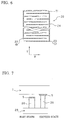
- the light 2 is introduced into the plate 1 for transmitting light from one end of the plate 1.
- the refractive index of the plate 1 is controlled so that all the light 2 totally reflects without penetrating the front surface 3 and the back surface 4 so as to pass inside the plate 1.
- any substance (displacement transmission in the present invention) 5 contacts at a distance not longer than a wave length
- the light 2 penetrates the back surface 4 and reaches the surface of the substance 5.
- the light 2 reflects on the surface of the substance 5 so as to become a scattering light 6 which penetrates into the plate 1.
- a part of the scattering light 6 totally reflects in the plate 1. However, most of the scattering light 6 penetrates the front surface 3 of the plate 1.
- the presence or the absence of a light emission (leaking light) of the light 2 on the front surface 3 of the plate 1 can be controlled by contacting or separating the substance 5 at the back surface 4 of the plate 1.
- the aforementioned presence or absence of the light emission acts as a picture element (pixell) as well as a conventional CRT and a liquid crystal display.
- a plurality of picture elements are disposed both vertically and horizontally. Switching-on and switching-off of each picture element is controlled so as to display any letter, figure, etc.
- the fundamental condition of coloring is determined by a mixing method of R (red), G (green), and B (blue).
- T is a frequency of color emission.
- the longest color-emitting period of R, G, and B is divided into three.
- the ratio of each of the color-emitting periods of R, G, and B is 1 : 1 : 1 as shown in Fig. 2, the color becomes white.
- the ratio of each of the color-emitting periods of R, G, and B is 4 : 1 : 5, the color corresponds to the ratio.
- the color may be controlled by controlling each of the periods of light emission of the three primary colors so as to correspond the period of contacting the displacement-transmitting portion 5 with the plate 1 to the frequency of the color-emitting period.
- the period of contacting the displacement-transmitting portion 5 with the plate 1 may be controlled so as to correspond the period of light emission to the frequency of the color-emitting period.
- the present invention advantageously does not require to increase the number of picture elements for a colored screen in comparison with a monochrome screen.
- Fig. 1 is a schematic showing an embodiment of a display element (element A) of the present invention.
- the left element is in a rest condition, and the right element is in an excited condition.
- an actuator 10 includes a piezoelectric film 11 made of ceramic and a pair of electrodes 12 and 13 covering each surface of the piezoelectric film 11. Under each of the actuator 10 is disposed a substrate 16 having a movable portion 14 and a fixed portion 15. The lower electrode 13 of the actuator 10 contacts with the movable portion 14 so as to directly support the actuator 10.
- the substrate 16 is made of ceramic and has a unitary structure including the movable portion 14 and the fixed portion 15. Further, the substrate 16 preferably has a cavity 17 so that the movable portion 14 is thin.
- the fixed portion 15 is disposed so as to surround the movable portion 14.
- a metallic fixed portion 15 may fix a ceramic vibrating portion 14.
- the fixed portion 15 is metallic, the surface of the vibrating portion 14 to be connected to the fixed portion is metallized.
- the metallized layer is soldered to the fixed portion 15.
- the fixed portion 15 may be made of metal such as stainless steel and iron.
- the fixed portion 15 is disposed so as to surround the movable portion 14. However, the fixed portion 15 may not support the movable portion 14 at all the circumference thereof, and the fixed portion 15 has only to support at least a part of the movable portion 14. In Fig. 1, only a part of the movable portion 14 is supported by the fixed portion 15.
- a displacement-transmitting portion 5 is connected so as to enlarge the area for contacting with the plate 1 to a predetermined degree.
- the displacement-transmitting portion 5 is disposed close to the plate 1 when the actuator is in a standing condition.
- the displacement-transmitting portion 5 contacts to the plate 1 at a distance of at most the wave length of the light.
- the displacement-transmitting portion 5 is formed of a member having a triangle cross-section.
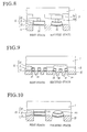
- Fig. 4 shows another embodiment of a display element of the present invention.
- the displacement-transmitting portion 5 includes a planar member 5a and a spherical member 5b.
- Fig. 5 shows still another embodiment of a display element of the present invention.
- the displacement-transmitting portion 5 includes a planar member 5a and a spherical member 5b as well as the embodiment in Fig. 4. Further, the embodiment shows the reversed disposition of the actuators 10 and the substrate 16 in contrast with Fig. 1 and Fig. 4.
- the stationary portion 15 is not necessarily connected to the movable portion 14. The stationary portion 15 may just contact with the movable portion 14.
- Fig. 8 shows another embodiment of a display element of the present invention.
- the positional relation of the actuator 10 with the substrate 16 is the same as that of Fig. 4.
- the actuator 10 flexes in the direction opposite to that of Fig. 4.
- Fig. 9 shows another embodiment of a display element of the present invention.
- one picture element has three actuators 10 having a piezoelectric film 11 and a pair of electrodes 12, 13.
- a movable portion 14 includes three thin plate portions 30 and a plurality of thick plate portions between the thin plate portions 30. In this arrangement, the size of the thin plate portions 30 effectively decreases.
- the displacement-transmitting portion 5 is disposed close to the plate 1 when the actuator 10 is in a standing condition, and the displacement-transmitting portion 5 is disposed so as to contact with the plate 1 at a distance not longer than the wave length of the light.
- Figs. 8 and 9 it is also possible to dispose the displacement-transmitting portion 5 so as to contact with the plate 1 at a distance not longer than the wave length of the light when the actuator 10 is in a standing condition and so as to be close to the plate 1 when the actuator 10 is in an excited condition.
- the contact and separation of the displacement-transmitting portion 5 with the plate 1 can be controlled by a direction of the polarization of the piezoelectric film and a direction of the electric field during driving.
- Fig. 6 shows an embodiment of a laminated actuator of a display element (element C) of the present invention.
- the laminated actuator 20 has a laminated piezoelectric body 24 including a plurality of ceramic piezoelectric layers 21, a plurality of electrode layers 22, and a plurality of electrode layers 23, wherein the piezoelectric layers 21 and the electrode layers 22 and 23 are laminated.
- the electrode layers include a positive electrode 22 having a shape of connected layers and a negative electrode 23 having a shape of connected layers.
- the layers forming the positive electrode 22 and the layers forming the negative electrode 23 are independently connected so as to have the same polarities alternately.
- the laminated piezoelectric body 24 having the aforementioned structure has both of a perpendicular and parallel directions of displacement to the direction of the lamination.
- the direction of the lamination is the direction Y.
- the size of the laminated piezoelectric body 24 should be enlarged to the direction Y in comparison with the size of the surface of the laminated layers.
- the amount of the displacement of the laminated piezoelectric body 24 equals to the total of the amount of the displacement in the direction of the thickness of each piezoelectric layer 21.
- the generating power equals to the total of the number of laminated layers.
- the size of the laminated piezoelectric body 24 should be reduced to the direction Y in comparison with the size of the surface of the laminated layers. In other words, the size of the laminated piezoelectric body 24 should be enlarged along the direction X.
- the amount of the displacement of the laminated piezoelectric body 24 equals to the amount of the displacement of each piezoelectric layer 21.
- the total displacement is proportional to the number of laminations.
- the displacement-transmitting portion 5 should be separated from the plate 1 in a rest condition.
- the displacement-transmitting portion 5 should contact to the plate 1. That is, the displacement-transmitting portion 5 should be separated from the plate 1 in an excited condition in which the light is not emitted.
- the laminated actuator 20, as shown in Fig. 6, for a display element (element C) does not include a movable portion as in element A.
- the actuator 20 is supported by the fixed portion 25.
- the movable portion 14 preferably has a planar shape since the shape is suitable for the flexing.
- the thickness of the plate preferably ranges from 1 to 100 ⁇ m, more preferably from 3 to 50 ⁇ m, furthermore preferably from 5 to 20 ⁇ m.
- the flexing portion 14 is preferably made of a material having high thermal resistance so as to prevent the flexing portion from thermally degenerating during forming the piezoelectric film 11 when the actuator 10 is placed directly on the flexing portion 14 without any material therebetween having low heat resistance, such as an organic adhesive.
- the flexing portion 14 is preferably made of an electrically insulated material. This is because the upper electrode 12 and the lower electrode 13 are electrically isolated when the upper electrode 12 and the lower electrode 13 of the actuator 10 supported directly by the flexing portion, leads connected to these electrodes, lead terminals, and the like are formed on the surface of the flexing portion 14. Therefore, the flexing portion 14 may be made of a metal having high thermal resistance, or a material such as enameled material which has a metal covered with ceramic such as glass. Most preferably, the flexing portion 14 is made of ceramic.
- stabilized zirconia aluminum oxide, magnesium oxide, mullite, aluminum nitride, silicon nitride, glass, or the like can be suitably used for the vibrating portion 14.
- Stabilized zirconia is especially preferable because it has high mechanical strength and high toughness even if the vibrating portion is thin and has limited reactivity against a piezoelectric film and electrodes, etc.
- Stabilized zirconia includes fully stabilized zirconia and partially stabilized zirconia. Stabilized zirconia does not cause phase transition since it has a crystallite of cubic phase. On the other hand, zirconium oxide causes phase transition between monoclinic crystals and tetragonal crystals at around 1000°C. This phase transition may generate cracks. Stabilized zirconia contains 1- 30% by mole of calcium oxide, magnesium oxide, yttrium oxide, scandium oxide, ytterbium oxide, cerium oxide, or a stabilizer such as rare earth metal oxide. Preferably, the stabilizer contains yttrium oxide so as to enhance mechanical strength of the vibrating portion.
- the amount of yttrium oxide contained in the stabilizer ranges preferably from 1.5 to 6% by mole, more preferably from 2 to 4% by mole.
- the main crystalline phase may be a mixture of cubic crystals and monoclinic crystals, a mixture of tetragonal crystals and monoclinic crystals, a mixture of cubic crystals, tetragonal crystals, and monoclinic crystals, etc.
- the main crystalline phase is tetragonal crystals or a mixture of tetragonal crystals and cubic crystals.
- Ceramic for the flexing portion 14 preferably contains 0.5 - 5% by weight of silicon oxide, more preferably 1 - 3% by weight, because silicon oxide prevents an excessive reaction between the vibrating portion 14 and the actuator 10 upon forming the actuator 10 by thermal treatment and gives excellent properties as an actuator.
- the vibrating portion 14 is made of ceramic, numerous crystalline particles compose the vibrating portion.
- the average diameter of the particles ranges preferably from 0.05 to 2 ⁇ m, more preferably from 0.1 to 1 ⁇ m.
- the stationary portion 15 is preferably made of ceramic.
- the ceramic material for the stationary portion 15 may be the same as that of the moving portion 14, or may be different from that of the moving portion 14.
- Stabilized zirconia, aluminum oxide, magnesium oxide, mullite, aluminum nitride, silicon nitride, glass, or the like, is suitable for the ceramic for the stationary portion 15 as well as a material for the moving portion 14.
- a shape of a cavity 17 is not limited.
- a shape of a horizontal or vertical cross section of the cavity may be, for example, a circle, an oval, a polygon including a square and a rectangle, or a complex shape of combination thereof.
- the edge of each corner is preferably removed so that each of the corners has a round shape.
- the actuator 10 includes a piezoelectric film 11, the upper electrode 12 covering at least a part of a surface 11s of the piezoelectric film 11, and the lower electrode 13 covering at least a part of the other surface 11t of the piezoelectric film 11.
- the lower electrode 13 covers at least a part of the surface 14s of the moving portion 14.
- the piezoelectric film 11 exhibits flexing displacement by applying voltage into the upper electrode 12 and the lower electrode 13.
- the piezoelectric film 11 preferably exhibits flexing displacement in the direction of its thickness.
- the flexing displacement of the piezoelectric film 11 causes the motion of the displacement-transmitting portion 5 in the direction of the thickness of the piezoelectric film 11, and the displacement-transmitting portion 5 contacts with the plate 1.
- the piezoelectric film 11 preferably has a thickness of 5 - 100 ⁇ m, more preferably 5 - 50 ⁇ m, furthermore preferably 5 - 30 ⁇ m.
- the piezoelectric film 11 may be suitably made of piezoelectric ceramic.
- the piezoelectric film 11 may be made of ceramic having electrostriction or ceramic having ferroelectricity.
- the piezoelectric film may be made of a material that requires a treatment for polarization and a material that does not require a treatment for polarization.
- the material is not limited to ceramic and may be a piezoelectric body including a polymer represented by PVDF (polyvinylidene fluoride) or a composite body of a polymer and ceramic.
- the ceramic for a piezoelectric film 11 may contain, for example, lead zirconate (PZT), lead magnesium niobate, lead nickel niobate, lead zinc niobate, lead manganese niobate, lead antimony stanate, lead titanate, barium titanate, lead magnesium tungstate, lead cobalt niobate, or any combination thereof.
- PZT lead zirconate
- lead magnesium niobate lead nickel niobate
- lead zinc niobate lead manganese niobate
- lead antimony stanate lead titanate
- barium titanate barium titanate
- lead magnesium tungstate lead cobalt niobate, or any combination thereof.
- a ceramic may contain not less than 50% by weight of a compound consisting of these as a main component.
- a ceramic containing lead zirconate can be preferably used.
- the aforementioned ceramic may be further include oxides of lanthanum, calcium, strontium, molybdenum, tungsten, barium, niobium, zinc, nickel, manganese, or the like; a combination thereof; or other compounds.
- the piezoelectric film 11 may be dense or may be porous.
- a porous piezoelectric film preferably has a porosity not more than 40%.
- a piezoelectric film 21 constitutes a part of the laminated actuator 20 in the display element of the embodiments C and in the display apparatus including it.
- the piezoelectric film 21 has a similar quality of a material and similar properties of the aforementioned piezoelectric film 11.
- Each of the upper electrode 12 and the lower electrode 13 has a suitable thickness depending on its application. However, the thickness ranges preferably from 0.1 to 50 ⁇ m.
- the upper electrode 12 is made of electrically conductive metal which is solid at room temperature.
- the upper electrode 12 is made of a metallic simple substance of aluminum, titanium, chromium, iron, cobalt, nickel, copper, zinc, niobium, molybdenum, ruthenium, rhodium, silver, tin, tantalum, tungsten, iridium, platinum, gold, lead, or the like; or an alloy thereof. Needless to say, these elements may be contained in any combination.
- the lower electrode 13 preferably made of a simple substance containing metal having a high melting point, such as platinum, ruthenium, rhodium, palladium, iridium, titanium, chromium, molybdenum, tantalum, tungsten, nickel, cobalt; or an alloy thereof. Needless to say, these metals each having a high melting point may be contained in any combination.
- a metal belonging to a platinum group such as platinum, rhodium, palladium, or an alloy containing these metals, such as silver-platinum, platinum-palladium is suitably used for the main component of a material for the electrode.
- a metal durable in an oxidizing atmosphere at high temperatures is preferably used for the lower electrode 13 because the lower electrode 13 is sometimes exposed to heat at a high temperature upon thermal treatment for the piezoelectric film 11.
- a material suitably used for the lower electrode may be a cermet containing a metal having a high melting point and a ceramic such as alumina, zirconium oxide, silicon oxide, and glass.
- the electrode layers 22 and 23 constituting a part of the laminated actuator 20 use the same material as that of the aforementioned upper electrode 12 and the lower electrode 13.
- the electrode layers 22 and 23 are thermally treated simultaneously with firing the piezoelectric layer 21 or at about the same temperature.
- the fixed portion 25 may be formed of the same material as the aforementioned material for the fixing portion 15.
- the fixed portion 25 is preferably a part of the laminated actuator 20.
- the upper electrode 12 of the actuator 10, the flexing portion 14, or the displacement-transmitting portion 5 connected with the laminated actuator 20 contacts to the back surface 4 of the plate 1 corresponding to the displacement of the actuator 10 or the laminated actuator 20.
- the dlsplacement-transmitting portion 5 is for reflecting the light 2 penetrating the back surface 4 of the plate 1 and for making the area contacting with the plate 1 larger than the predetermined size. That is, the area of light emission is determined by the area of contacting the displacement-transmitting portion 5 and the plate 1.
- Contact means that the displacement-transmitting portion 5 and the plate 1 are placed within the distance not longer than the wave length of the light.
- the displacement-transmitting portion 5 preferably has a sufficient hardness to transmit the displacement of the actuator 10 to the plate 1 directly.
- the material for the displacement-transmitting portion 5 is preferably rubber, organic resin, glass, etc., to give the aforementioned properties.
- the material may be the electrode layers itself, the piezoelectric body, the aforementioned ceramics, or the like.
- the surface, to contact with the plate 1, of the displacement-transmitting portion 5 is satisfactorily flat in comparison with the amount of displacement of the actuator 10.
- the unevenness is preferably not larger than 1 ⁇ m, more preferably not larger than 0.5 ⁇ m, furthermore preferably not larger than 0.1 ⁇ m.
- the flatness is important to reduce the gap when the displacement-transmitting portion 5 contacts with the plate 1. Therefore, the degree of unevenness is not limited to the aforementioned ranges when the contacting portion is deformed in a contacting condition.
- an actuator 10 the plate 1 and a sidewall define a cavity where a light-transmitting liquid 32 is present.
- an upper electrode 12 serves as a displacement-transmitting means 5, and the liquid 32 may be regarded as a part of the plate 1.
- the liquid 32 effectively reduces the gap between the actuator 10 and the plate 1 or between the displacement-transmitting means 5 and the plate 1 so as to easily switch the light.
- Liquid 32 includes, for example, an organic solvent having a low vapor pressure, an oil, etc.
- the cavity is preferably sealed so as to prevent the liquid from vaporizing.
- a sidewall having a desired height may be formed in the top periphery of the actuator 10. The sidewall may touch the plate 1.
- the sidewall may leave a gap toward the plate 1.
- the displacement-transmitting means 5 may have a surface having depressions and protrusion, and the liquid may be held in the depressions.
- the displacement-transmitting means may have open pores, and the liquid 32 may be impregnated in the open pores. In these cases, the liquid 32 is held by the surface tension thereof.
- the plate 1 of the present embodiments has a refractive index for total reflection of the light introduced into the plate 1 at the front surface 3 and the back surface 4 of the plate 1.
- the material is not limited as long as the material has such properties.
- the popular materials are, for example, glass, quartz, translucent plastic, translucent ceramic, a laminated body of layers having varied refractive indexes, and a plate having a coating layer on the surface.
- the present invention provides a display apparatus capable of expressing any letter, any figure, etc., as well as a conventional CRT and a liquid crystal, by disposing a predetermined number of aforementioned display elements suitably and controlling the switching-on and switching-off of each of the display elements.
- the number of display elements is not necessarily plural and may be only one.
- Shaped layers of green sheet or green tape are laminated by hot pressing or the like and then sintered to obtain a unitary substrate 16.
- a throughhole having a predetermined shape is made in advance before laminating so that the cavity 17 is formed.
- the shaped layers are formed by press molding, slip casting, injection molding, or the like.
- the cavity may be formed by machining such as cutting, machining of metals, laser machining, blanking by press working, or the like.
- the actuator 10 is formed on the movable portion 14.
- a piezoelectric body is formed by press molding using a mold, tape forming using a slurry, or the like.
- the green piezoelectric body is laminated on the movable portion 14 of the green substrate by hot pressing and is sintered simultaneously so as to form a substrate and a piezoelectric body. This method requires to form the electrodes 12 and 13 in advance on the piezoelectric body by one of the methods for forming a film described later.
- a temperature for sintering a piezoelectric film 11 is suitably determined depending on the materials composing the film, the temperature ranges generally from 800° C to 1400°C, preferably from 1000°C to 1400°C.
- the piezoelectric film is sintered under the presence of a source for evaporating the material of the piezoelectric film so as to control the composition of the piezoelectric film 11.
- a method for forming a film the lower electrode 13, the piezoelectric film 11, and the upper electrode 12 are laminated on the movable portion 14 in this order to form the actuator 10.
- a method for forming a film may be suitably selected from methods in conventional art, for example, a method for forming a thick film such as screen printing, an applying method such as dipping, a method for forming a thin film such as ion beam, sputtering, vacuum deposition, ion plating, chemical vapor deposition (CVD), plating.
- a method for forming a film is not limited to these methods.
- the lower electrode 13, the unillustrated lead, and terminal pad are simultaneously applied to the substrate by screen printing.
- the piezoelectric film 11 is formed by a method for forming a thick film, such as screen printing or the like. These methods use a paste or a slurry containing ceramic powders of the material for the piezoelectric film as a main component. Therefore, the piezoelectric film 11 is formed on the substrate so as to have excellent piezoelectric properties. Forming a piezoelectric film by one of these methods for forming films does not require any adhesive, and the actuator 10 can be unitarily connected with the vibrating portion 14. Therefore, such a method is particularly preferable in view of excellent reliability, excellent reproducibility, and easy integration. A shape of such a film may have a suitable pattern. The pattern may be formed by a method such as screen printing or photolithography or by removing unnecessary parts by machining such as laser machining, slicing, ultrasonication. Among these, screen printing is most favorable.
- the shapes for the piezoelectric film, the upper electrode, and the lower electrode are not limited at all, and any shape may be selected depending on its application.
- they may be a polygon such as a triangle and a square, a curved shape such as a circle, an oval, and a torus, a comblike shape, a lattice, or a combination thereof to form a special shape.
- Each of the films 11, 12, 13, which are thus formed on a substrate may be thermally treated, respectively, each time that the film is formed, so that the film and substrate are unitarily connected. Alternatively, after all the films are formed, the films may be thermally treated altogether so as to integrally connect the films to the substrate.
- the thermal treatment is not always necessary to form these electrodes unitarily.
- the displacement-transmitting member made of an aforementioned material may be laminated on the actuator 10 by means of an adhesive.
- a solution or a slurry of an aforementioned material is coated on the actuator 10. It is not always necessary to cut the displacement-transmitting portion so as to have almost the same shape as the actuator 10. However, it is preferable to cut the layer of the displacement-transmitting portion 5 or to notch the layer so as to enhance the efficiency of the displacement of the actuator 10.
- the predetermined distance between the displacement-transmitting portion 5 and the plate 1 after assembling is required to be small in comparison with the degree of displacement of the actuator 10.
- a gap-forming member having a predetermined size is disposed in the portion without the actuator 10 so that the fixing portion 15 is tightly connected to the plate 1.
- the laminated actuator 20 shown in Fig. 6 can be produced in the same manner as the actuator 10.
- the laminated actuator 20 can be connected to the displacement-transmitting portion 5 can be supported by the fixed portion 25 in the same manner as the aforementioned Inventions A and B.
- the laminated actuator 20 preferably has a fixed portion 25 as a part of the laminated actuator. Therefore, the fixed portion 25 is not always necessary.
- the predetermined number of the piezoelectric layers 21 each having an electrode on one surface thereof are laminated to form a laminated body, which is fired and then cut a predetermined portion of the thickness of the laminated body so as to form a plurality of laminated actuators 20.
- the piezoelectric layers 21 and the electrode layers 22 and 23 are laminated alternately on the substrate which does not exist during firing, followed by exfoliating the laminated body from the substrate so as to fire the laminated body. Further, the laminated body may be cut before firing.
- a picture element may have a dimension ranging from 0.3 mm to 3 mm.
- a larger picture element is suitable for a larger display apparatus.
- the display apparatus may have a plurality of display elements arranged a number N in vertical directions and a number M in lateral directions. All of the display elements may be treated as a whole. However, all of the display elements may not necessarily treated as a whole.
- One unit may have the display elements having a number A in vertical directions and a number B in lateral directions, and a plurality of the units may be combined to form the display apparatus. In this case, A is a divisor of N, and B is a divisor of M.
- the present invention provides a display element and a display apparatus both having quick response, consuming little electric power and having a small size, and having high brightness of a screen. Further, a colored screen does not need to increase the number of picture elements in comparison with a monochrome screen.
- the display element and the display apparatus can be applied to other articles such as a switch for light.
Priority Applications (1)
| Application Number | Priority Date | Filing Date | Title |
|---|---|---|---|
| EP01120967A EP1168283A1 (de) | 1994-04-01 | 1995-03-31 | Anzeigenelement und Anzeigevorrichtung |
Applications Claiming Priority (3)
| Application Number | Priority Date | Filing Date | Title |
|---|---|---|---|
| US22101594A | 1994-04-01 | 1994-04-01 | |
| US221015 | 1994-04-01 | ||
| EP95302191A EP0675477B1 (de) | 1994-04-01 | 1995-03-31 | Anzeigenelement und Anzeigevorrichtung |
Related Parent Applications (1)
| Application Number | Title | Priority Date | Filing Date |
|---|---|---|---|
| EP95302191A Division EP0675477B1 (de) | 1994-04-01 | 1995-03-31 | Anzeigenelement und Anzeigevorrichtung |
Related Child Applications (1)
| Application Number | Title | Priority Date | Filing Date |
|---|---|---|---|
| EP01120967A Division EP1168283A1 (de) | 1994-04-01 | 1995-03-31 | Anzeigenelement und Anzeigevorrichtung |
Publications (2)
| Publication Number | Publication Date |
|---|---|
| EP0927984A1 true EP0927984A1 (de) | 1999-07-07 |
| EP0927984B1 EP0927984B1 (de) | 2001-11-28 |
Family
ID=22825984
Family Applications (3)
| Application Number | Title | Priority Date | Filing Date |
|---|---|---|---|
| EP95302191A Expired - Lifetime EP0675477B1 (de) | 1994-04-01 | 1995-03-31 | Anzeigenelement und Anzeigevorrichtung |
| EP99107101A Expired - Lifetime EP0927984B1 (de) | 1994-04-01 | 1995-03-31 | Anzeigenelement und Anzeigevorrichtung |
| EP01120967A Withdrawn EP1168283A1 (de) | 1994-04-01 | 1995-03-31 | Anzeigenelement und Anzeigevorrichtung |
Family Applications Before (1)
| Application Number | Title | Priority Date | Filing Date |
|---|---|---|---|
| EP95302191A Expired - Lifetime EP0675477B1 (de) | 1994-04-01 | 1995-03-31 | Anzeigenelement und Anzeigevorrichtung |
Family Applications After (1)
| Application Number | Title | Priority Date | Filing Date |
|---|---|---|---|
| EP01120967A Withdrawn EP1168283A1 (de) | 1994-04-01 | 1995-03-31 | Anzeigenelement und Anzeigevorrichtung |
Country Status (4)
| Country | Link |
|---|---|
| US (2) | US5636072A (de) |
| EP (3) | EP0675477B1 (de) |
| JP (2) | JP3187669B2 (de) |
| DE (2) | DE69524266T2 (de) |
Cited By (1)
| Publication number | Priority date | Publication date | Assignee | Title |
|---|---|---|---|---|
| US6381381B1 (en) | 1998-01-20 | 2002-04-30 | Seiko Epson Corporation | Optical switching device and image display device |
Families Citing this family (71)
| Publication number | Priority date | Publication date | Assignee | Title |
|---|---|---|---|---|
| US5771321A (en) * | 1996-01-04 | 1998-06-23 | Massachusetts Institute Of Technology | Micromechanical optical switch and flat panel display |
| JP3585310B2 (ja) * | 1996-02-20 | 2004-11-04 | 日本碍子株式会社 | マルチダイヤフラム構造体の製造法 |
| TW357271B (en) * | 1996-02-26 | 1999-05-01 | Seiko Epson Corp | Light regulator, display and the electronic machine |
| JP3517535B2 (ja) * | 1996-07-10 | 2004-04-12 | 日本碍子株式会社 | 表示装置 |
| US5953469A (en) * | 1996-10-29 | 1999-09-14 | Xeotron Corporation | Optical device utilizing optical waveguides and mechanical light-switches |
| US6091182A (en) * | 1996-11-07 | 2000-07-18 | Ngk Insulators, Ltd. | Piezoelectric/electrostrictive element |
| JP3904240B2 (ja) * | 1996-11-29 | 2007-04-11 | 日本碍子株式会社 | セラミック素子 |
| US6028978A (en) * | 1996-12-16 | 2000-02-22 | Ngk Insulators, Ltd. | Display device having a colored layer disposed between a displacement transmitting section and an optical waveguide plate |
| US6211853B1 (en) | 1996-12-16 | 2001-04-03 | Ngk Insulators, Ltd. | Optical waveguide display with voltage-modulated controlled movable actuators which cause light leakage in waveguide at each display element to provide gradation in a display image |
| JPH10326088A (ja) | 1997-03-24 | 1998-12-08 | Ngk Insulators Ltd | ディスプレイの駆動装置及びディスプレイの駆動方法 |
| JPH10307541A (ja) | 1997-05-07 | 1998-11-17 | Ngk Insulators Ltd | ディスプレイ用光導波板 |
| JP3224209B2 (ja) * | 1997-05-07 | 2001-10-29 | 日本碍子株式会社 | ディスプレイ用光導波板 |
| US6281868B1 (en) | 1997-05-30 | 2001-08-28 | Ngk Insulators, Ltd. | Display |
| JP3787983B2 (ja) | 1997-06-18 | 2006-06-21 | セイコーエプソン株式会社 | 光スイッチング素子、画像表示装置及び投射装置 |
| JP3437743B2 (ja) | 1997-07-18 | 2003-08-18 | 日本碍子株式会社 | ディスプレイの駆動装置及びディスプレイの駆動方法 |
| GB2328312B (en) * | 1997-08-14 | 1999-08-04 | John Quentin Phillipps | Mirror controlled display device |
| WO1999024859A1 (fr) * | 1997-11-06 | 1999-05-20 | Ngk Insulators, Ltd. | Affichage et procede de fabrication de ce dernier |
| WO1999028890A1 (en) * | 1997-11-29 | 1999-06-10 | Koninklijke Philips Electronics N.V. | Display device comprising a light guide |
| DE69828034T2 (de) * | 1998-01-20 | 2005-04-21 | Seiko Epson Corp | Optische schaltvorrichtung,bildanzeige und projektionsvorrichtung |
| US6146716A (en) * | 1998-06-26 | 2000-11-14 | Sri International | Conservatively printed displays and methods relating to same |
| JP3762568B2 (ja) * | 1998-08-18 | 2006-04-05 | 日本碍子株式会社 | ディスプレイの駆動装置及びディスプレイの駆動方法 |
| US6249370B1 (en) | 1998-09-18 | 2001-06-19 | Ngk Insulators, Ltd. | Display device |
| WO2000021877A1 (fr) * | 1998-10-13 | 2000-04-20 | Seiko Epson Corporation | Micromachine et procede de fabrication correspondant |
| US6690344B1 (en) | 1999-05-14 | 2004-02-10 | Ngk Insulators, Ltd. | Method and apparatus for driving device and display |
| DE19931008C1 (de) * | 1999-07-06 | 2000-08-31 | Daimler Chrysler Ag | Fahrzeugleuchteneinheit mit einem Lichtleitersystem |
| US6700554B2 (en) * | 1999-12-04 | 2004-03-02 | Lg. Philips Lcd Co., Ltd. | Transmissive display device using micro light modulator |
| EP1158333A1 (de) | 1999-12-27 | 2001-11-28 | Ngk Insulators, Ltd. | ANZEIGEVORRICHTUNG UND DAZUGEHöRIGES HERSTELLUNGSVERFAHREN |
| WO2001048534A1 (fr) * | 1999-12-27 | 2001-07-05 | Ngk Insulators, Ltd. | Dispositif d'affichage et procede de fabrication correspondant |
| JP3571693B2 (ja) * | 1999-12-27 | 2004-09-29 | 日本碍子株式会社 | 表示装置 |
| CN1160684C (zh) * | 2000-02-24 | 2004-08-04 | 皇家菲利浦电子有限公司 | 包括光波导的显示器件 |
| JP2001324960A (ja) * | 2000-03-10 | 2001-11-22 | Ngk Insulators Ltd | ディスプレイシステム及びディスプレイの管理方法 |
| US6453100B1 (en) | 2000-03-27 | 2002-09-17 | Ngk Insulators, Ltd. | Display device and method for producing the same |
| JP4433673B2 (ja) * | 2000-12-22 | 2010-03-17 | 日本碍子株式会社 | 光スイッチ |
| JP2002196263A (ja) * | 2000-12-26 | 2002-07-12 | Ngk Insulators Ltd | ディスプレイ装置 |
| JP2002258179A (ja) * | 2000-12-27 | 2002-09-11 | Ngk Insulators Ltd | 反射型表示装置 |
| JP2002287042A (ja) * | 2001-03-27 | 2002-10-03 | Ngk Insulators Ltd | 表示装置 |
| US7102632B2 (en) * | 2001-06-05 | 2006-09-05 | Eastman Kodak Company | Method for saving power in an organic electroluminescent display |
| US6879753B2 (en) | 2001-06-15 | 2005-04-12 | Ngk Insulators, Ltd. | Display device |
| JP4074493B2 (ja) | 2001-08-31 | 2008-04-09 | 日本碍子株式会社 | セラミック素子 |
| US20030043449A1 (en) * | 2001-09-03 | 2003-03-06 | Ngk Insulators, Ltd. | Display device and method for producing the same |
| US6798959B2 (en) | 2001-09-03 | 2004-09-28 | Ngk Insulators, Ltd. | Display device and method for producing the same |
| JP2003076286A (ja) * | 2001-09-06 | 2003-03-14 | Ngk Insulators Ltd | ディスプレイ装置用の冷却システム |
| ATE330304T1 (de) * | 2001-12-10 | 2006-07-15 | Koninkl Philips Electronics Nv | Anzeigetafel mit einem lichtleiter |
| WO2003063115A2 (en) * | 2002-01-22 | 2003-07-31 | Koninklijke Philips Electronics N.V. | Display device comprising a light guide |
| JP2005300560A (ja) | 2002-02-22 | 2005-10-27 | Mitsuteru Kimura | ディスプレイ装置 |
| US20060182389A1 (en) * | 2002-03-26 | 2006-08-17 | Duine Peter A | Display device comprising a light transmitting first plate and light-absorbing means |
| CN1656408A (zh) * | 2002-05-21 | 2005-08-17 | 皇家飞利浦电子股份有限公司 | 包括光导板的显示面板 |
| US20030227447A1 (en) | 2002-06-04 | 2003-12-11 | Ngk Insulators, Ltd. | Display device |
| US7006061B2 (en) | 2002-06-04 | 2006-02-28 | Ngk Insulators, Ltd. | Display device |
| TW200413776A (en) | 2002-11-05 | 2004-08-01 | Matsushita Electric Ind Co Ltd | Display element and display using the same |
| WO2004107298A1 (en) | 2003-05-22 | 2004-12-09 | Koninklijke Philips Electronics N.V. | Line-at-a-time foil display |
| EP1640787B1 (de) | 2003-06-20 | 2009-04-01 | Sharp Kabushiki Kaisha | Anzeige |
| JP2005301222A (ja) | 2004-03-19 | 2005-10-27 | Sharp Corp | 表示装置 |
| KR20060116102A (ko) * | 2005-05-09 | 2006-11-14 | 삼성전자주식회사 | 백라이트 어셈블리 및 이를 갖는 표시 장치 |
| US7751663B2 (en) | 2006-09-21 | 2010-07-06 | Uni-Pixel Displays, Inc. | Backside reflection optical display |
| US20100081032A1 (en) * | 2007-06-29 | 2010-04-01 | Subhasish Mukerjee | Glass Seal Containing Zirconia Powder and Fiber for a Solid Oxide Fuel Cell Stack |
| WO2009006318A1 (en) | 2007-06-29 | 2009-01-08 | Artificial Muscle, Inc. | Electroactive polymer transducers for sensory feedback applications |
| US20100214282A1 (en) | 2009-02-24 | 2010-08-26 | Dolby Laboratories Licensing Corporation | Apparatus for providing light source modulation in dual modulator displays |
| EP2239793A1 (de) | 2009-04-11 | 2010-10-13 | Bayer MaterialScience AG | Elektrisch schaltbarer Polymerfilmaufbau und dessen Verwendung |
| PL2466994T3 (pl) | 2010-12-17 | 2020-07-27 | Dolby Laboratories Licensing Corporation | Modulacja kropek kwantowych dla wyświetlaczy |
| KR20140008416A (ko) | 2011-03-01 | 2014-01-21 | 바이엘 인텔렉쳐 프로퍼티 게엠베하 | 변형가능한 중합체 장치 및 필름을 제조하기 위한 자동화 제조 방법 |
| CN103703404A (zh) * | 2011-03-22 | 2014-04-02 | 拜耳知识产权有限责任公司 | 电活化聚合物致动器双凸透镜系统 |
| EP2828901B1 (de) | 2012-03-21 | 2017-01-04 | Parker Hannifin Corporation | Rolle-an-rolle-herstellungsverfahren zur herstellung selbstheilender elektroaktiver polymervorrichtungen |
| KR20150031285A (ko) | 2012-06-18 | 2015-03-23 | 바이엘 인텔렉쳐 프로퍼티 게엠베하 | 연신 공정을 위한 연신 프레임 |
| KR102118309B1 (ko) | 2012-09-19 | 2020-06-03 | 돌비 레버러토리즈 라이쎈싱 코오포레이션 | 양자점/리모트 인광 디스플레이 시스템 개선 |
| WO2014066576A1 (en) | 2012-10-24 | 2014-05-01 | Bayer Intellectual Property Gmbh | Polymer diode |
| BR112015020571B1 (pt) | 2013-03-08 | 2022-04-12 | Dolby Laboratories Licensing Corporation | Método para acionamento de um monitor de escurecimento local, meio de armazenamento não transitório legível por computador e aparelho |
| JP6441956B2 (ja) | 2014-03-26 | 2018-12-19 | ドルビー ラボラトリーズ ライセンシング コーポレイション | 各種ディスプレイにおけるグローバル光補償 |
| EP3633663A1 (de) | 2014-08-21 | 2020-04-08 | Dolby Laboratories Licensing Corp. | Techniken zur doppelmodulation mit lichtumwandlung |
| KR20160089722A (ko) | 2015-01-20 | 2016-07-28 | 삼성전자주식회사 | 화면 표시 장치 및 방법 |
| CN106710637A (zh) * | 2016-11-30 | 2017-05-24 | 南京航空航天大学 | 一种基于压电叠堆的微位移定位机构 |
Citations (4)
| Publication number | Priority date | Publication date | Assignee | Title |
|---|---|---|---|---|
| US4113360A (en) * | 1977-03-28 | 1978-09-12 | Siemens Aktiengesellschaft | Indicating device for illustrating symbols of all kinds |
| EP0039883A1 (de) * | 1980-05-12 | 1981-11-18 | Siemens Aktiengesellschaft | Vorrichtung zur mehrfarbigen optischen Darstellung von Informationen |
| JPH0498102A (ja) * | 1990-08-16 | 1992-03-30 | Canon Inc | 積層圧電変位素子、それを用いた走査型トンネル顕微鏡及び記録再生装置 |
| EP0565883A2 (de) * | 1992-03-16 | 1993-10-20 | Rockwell International Corporation | Anisotroper Wandler |
Family Cites Families (6)
| Publication number | Priority date | Publication date | Assignee | Title |
|---|---|---|---|---|
| US3654476A (en) * | 1967-05-15 | 1972-04-04 | Bell Telephone Labor Inc | Solid-state television camera devices |
| US4280756A (en) * | 1979-01-02 | 1981-07-28 | Itek Corporation | Piezoelectric bi-morph mirror actuator |
| JPH07108102B2 (ja) * | 1990-05-01 | 1995-11-15 | 日本碍子株式会社 | 圧電/電歪膜型アクチュエータの製造方法 |
| US5210455A (en) * | 1990-07-26 | 1993-05-11 | Ngk Insulators, Ltd. | Piezoelectric/electrostrictive actuator having ceramic substrate having recess defining thin-walled portion |
| EP0526048B1 (de) * | 1991-07-18 | 1997-11-12 | Ngk Insulators, Ltd. | Piezoelektrischer/elektrostriktiver Element mit einem keramischen Substrat aus stabilisiertem Zirkoniumdioxid |
| JP2665106B2 (ja) * | 1992-03-17 | 1997-10-22 | 日本碍子株式会社 | 圧電/電歪膜型素子 |
-
1994
- 1994-12-02 JP JP29972094A patent/JP3187669B2/ja not_active Expired - Fee Related
-
1995
- 1995-03-31 DE DE69524266T patent/DE69524266T2/de not_active Expired - Fee Related
- 1995-03-31 EP EP95302191A patent/EP0675477B1/de not_active Expired - Lifetime
- 1995-03-31 EP EP99107101A patent/EP0927984B1/de not_active Expired - Lifetime
- 1995-03-31 DE DE69513427T patent/DE69513427T2/de not_active Expired - Fee Related
- 1995-03-31 EP EP01120967A patent/EP1168283A1/de not_active Withdrawn
- 1995-04-12 US US08/420,783 patent/US5636072A/en not_active Expired - Lifetime
-
1996
- 1996-10-21 US US08/734,195 patent/US5774257A/en not_active Expired - Fee Related
-
2000
- 2000-07-28 JP JP2000229646A patent/JP3499517B2/ja not_active Expired - Fee Related
Patent Citations (4)
| Publication number | Priority date | Publication date | Assignee | Title |
|---|---|---|---|---|
| US4113360A (en) * | 1977-03-28 | 1978-09-12 | Siemens Aktiengesellschaft | Indicating device for illustrating symbols of all kinds |
| EP0039883A1 (de) * | 1980-05-12 | 1981-11-18 | Siemens Aktiengesellschaft | Vorrichtung zur mehrfarbigen optischen Darstellung von Informationen |
| JPH0498102A (ja) * | 1990-08-16 | 1992-03-30 | Canon Inc | 積層圧電変位素子、それを用いた走査型トンネル顕微鏡及び記録再生装置 |
| EP0565883A2 (de) * | 1992-03-16 | 1993-10-20 | Rockwell International Corporation | Anisotroper Wandler |
Non-Patent Citations (2)
| Title |
|---|
| ANONYMOUS: "Ion Depletion Projection Display", IBM TECHNICAL DISCLOSURE BULLETIN, vol. 30, no. 6, NEW YORK, US, pages 43 - 44, XP002038194 * |
| PATENT ABSTRACTS OF JAPAN vol. 016, no. 330 (P - 1388) 17 July 1992 (1992-07-17) * |
Cited By (2)
| Publication number | Priority date | Publication date | Assignee | Title |
|---|---|---|---|---|
| US6381381B1 (en) | 1998-01-20 | 2002-04-30 | Seiko Epson Corporation | Optical switching device and image display device |
| US6438282B1 (en) | 1998-01-20 | 2002-08-20 | Seiko Epson Corporation | Optical switching device and image display device |
Also Published As
| Publication number | Publication date |
|---|---|
| DE69513427D1 (de) | 1999-12-30 |
| EP0675477B1 (de) | 1999-11-24 |
| EP0927984B1 (de) | 2001-11-28 |
| EP1168283A1 (de) | 2002-01-02 |
| JP3187669B2 (ja) | 2001-07-11 |
| US5774257A (en) | 1998-06-30 |
| JP3499517B2 (ja) | 2004-02-23 |
| DE69513427T2 (de) | 2000-05-04 |
| DE69524266T2 (de) | 2002-07-04 |
| US5636072A (en) | 1997-06-03 |
| EP0675477A1 (de) | 1995-10-04 |
| JPH07287176A (ja) | 1995-10-31 |
| DE69524266D1 (de) | 2002-01-10 |
| JP2001100123A (ja) | 2001-04-13 |
Similar Documents
| Publication | Publication Date | Title |
|---|---|---|
| EP0927984B1 (de) | Anzeigenelement und Anzeigevorrichtung | |
| US6249370B1 (en) | Display device | |
| US6091182A (en) | Piezoelectric/electrostrictive element | |
| EP0853252B1 (de) | Anzeigegerät | |
| US20030011284A1 (en) | Ceramic element, method for producing ceramic element, display device, relay device, and capacitor | |
| US5504388A (en) | Piezoelectric/electrostrictive element having electrode film(s) with specified surface roughness | |
| US6049158A (en) | Piezoelectric/electrostrictive film element having convex diaphragm portions and method of producing the same | |
| US6088893A (en) | Method for producing a piezoelectric/electrostrictive film-type element | |
| EP1998383B1 (de) | Verfahren zur herstellung eines keramikelements und keramikelement für gassensorbauteil, brennstoffzellenbauteil, filterbauteil, vielschichtpiezobauteil, einspritzvorrichtung und kraftstoffeinspritzsystem | |
| EP0667646A1 (de) | Piezoelektrisches/elektrostriktives Dünnfilmelement und Herstellungsverfahren | |
| EP1100291A1 (de) | Verbundsubstrat, dünnschichtelektrolumineszente vorrichtung dieses verwendend und herstellungsverfahren desselben | |
| JPH1078549A (ja) | 表示装置 | |
| US6724973B1 (en) | Display and its manufacturing method | |
| US20030175062A1 (en) | Piezoelectric/electrostrictive device | |
| EP1237205B1 (de) | Piezoelektrisches/elektrostriktives Bauelement zur Lichtreflexion sowie dessen Herstellungsverfahren | |
| EP1294029A2 (de) | Bauelement mit piezoelektrischem/elektrostriktivem Film | |
| KR20030038788A (ko) | 압전 박막 및 그 제조방법, 압전 박막을 구비한 압전소자, 압전 소자를 이용한 잉크 제트 헤드, 및 잉크 제트헤드를 구비한 잉크 제트식 기록 장치 | |
| JPH11339561A (ja) | セラミック素子、セラミック素子の製造方法、表示装置、リレー装置及びコンデンサ | |
| EP1294030A2 (de) | Piezoelektrisches/elektrostriktives Bauelement | |
| CN1132138C (zh) | 显示元件和显示设备 | |
| JPH11194723A (ja) | 表示装置 | |
| JP2004045445A (ja) | 表示装置 |
Legal Events
| Date | Code | Title | Description |
|---|---|---|---|
| PUAI | Public reference made under article 153(3) epc to a published international application that has entered the european phase |
Free format text: ORIGINAL CODE: 0009012 |
|
| AC | Divisional application: reference to earlier application |
Ref document number: 675477 Country of ref document: EP |
|
| AK | Designated contracting states |
Kind code of ref document: A1 Designated state(s): DE FR GB IT NL |
|
| 17P | Request for examination filed |
Effective date: 19990726 |
|
| 17Q | First examination report despatched |
Effective date: 20000705 |
|
| GRAG | Despatch of communication of intention to grant |
Free format text: ORIGINAL CODE: EPIDOS AGRA |
|
| DAX | Request for extension of the european patent (deleted) | ||
| GRAG | Despatch of communication of intention to grant |
Free format text: ORIGINAL CODE: EPIDOS AGRA |
|
| GRAG | Despatch of communication of intention to grant |
Free format text: ORIGINAL CODE: EPIDOS AGRA |
|
| GRAH | Despatch of communication of intention to grant a patent |
Free format text: ORIGINAL CODE: EPIDOS IGRA |
|
| GRAH | Despatch of communication of intention to grant a patent |
Free format text: ORIGINAL CODE: EPIDOS IGRA |
|
| GRAA | (expected) grant |
Free format text: ORIGINAL CODE: 0009210 |
|
| AC | Divisional application: reference to earlier application |
Ref document number: 675477 Country of ref document: EP |
|
| AK | Designated contracting states |
Kind code of ref document: B1 Designated state(s): DE FR GB IT NL |
|
| RIN1 | Information on inventor provided before grant (corrected) |
Inventor name: PELRINE, RONALD E. Inventor name: SHRADER, ERIC J. Inventor name: FROHBACH, HUGH Inventor name: TAKEUCHI, YUKIHISA Inventor name: SHIBATA, KAZUYOSHI |
|
| REG | Reference to a national code |
Ref country code: GB Ref legal event code: IF02 |
|
| REF | Corresponds to: |
Ref document number: 69524266 Country of ref document: DE Date of ref document: 20020110 |
|
| ET | Fr: translation filed |
Owner name: KONINKLIJKE PHILIPS ELECTRONICS N.V. |
|
| PLBE | No opposition filed within time limit |
Free format text: ORIGINAL CODE: 0009261 |
|
| STAA | Information on the status of an ep patent application or granted ep patent |
Free format text: STATUS: NO OPPOSITION FILED WITHIN TIME LIMIT |
|
| 26N | No opposition filed |
Opponent name: KONINKLIJKE PHILIPS ELECTRONICS N.V. |
|
| PGFP | Annual fee paid to national office [announced via postgrant information from national office to epo] |
Ref country code: NL Payment date: 20040318 Year of fee payment: 10 |
|
| PG25 | Lapsed in a contracting state [announced via postgrant information from national office to epo] |
Ref country code: IT Free format text: LAPSE BECAUSE OF NON-PAYMENT OF DUE FEES;WARNING: LAPSES OF ITALIAN PATENTS WITH EFFECTIVE DATE BEFORE 2007 MAY HAVE OCCURRED AT ANY TIME BEFORE 2007. THE CORRECT EFFECTIVE DATE MAY BE DIFFERENT FROM THE ONE RECORDED. Effective date: 20050331 |
|
| PG25 | Lapsed in a contracting state [announced via postgrant information from national office to epo] |
Ref country code: NL Free format text: LAPSE BECAUSE OF NON-PAYMENT OF DUE FEES Effective date: 20051001 |
|
| NLV4 | Nl: lapsed or anulled due to non-payment of the annual fee |
Effective date: 20051001 |
|
| PGFP | Annual fee paid to national office [announced via postgrant information from national office to epo] |
Ref country code: GB Payment date: 20080211 Year of fee payment: 14 |
|
| PGFP | Annual fee paid to national office [announced via postgrant information from national office to epo] |
Ref country code: FR Payment date: 20080307 Year of fee payment: 14 Ref country code: DE Payment date: 20080331 Year of fee payment: 14 |
|
| GBPC | Gb: european patent ceased through non-payment of renewal fee |
Effective date: 20090331 |
|
| REG | Reference to a national code |
Ref country code: FR Ref legal event code: ST Effective date: 20091130 |
|
| PG25 | Lapsed in a contracting state [announced via postgrant information from national office to epo] |
Ref country code: DE Free format text: LAPSE BECAUSE OF NON-PAYMENT OF DUE FEES Effective date: 20091001 |
|
| PG25 | Lapsed in a contracting state [announced via postgrant information from national office to epo] |
Ref country code: GB Free format text: LAPSE BECAUSE OF NON-PAYMENT OF DUE FEES Effective date: 20090331 Ref country code: FR Free format text: LAPSE BECAUSE OF NON-PAYMENT OF DUE FEES Effective date: 20091123 |