EP0923174B1 - Vorrichtung und Verfahren zur Temperaturkompensation von Laserdioden - Google Patents
Vorrichtung und Verfahren zur Temperaturkompensation von Laserdioden Download PDFInfo
- Publication number
- EP0923174B1 EP0923174B1 EP98304406A EP98304406A EP0923174B1 EP 0923174 B1 EP0923174 B1 EP 0923174B1 EP 98304406 A EP98304406 A EP 98304406A EP 98304406 A EP98304406 A EP 98304406A EP 0923174 B1 EP0923174 B1 EP 0923174B1
- Authority
- EP
- European Patent Office
- Prior art keywords
- value
- counting
- count value
- counter
- voltage
- Prior art date
- Legal status (The legal status is an assumption and is not a legal conclusion. Google has not performed a legal analysis and makes no representation as to the accuracy of the status listed.)
- Expired - Lifetime
Links
Images


Classifications
-
- H—ELECTRICITY
- H01—ELECTRIC ELEMENTS
- H01S—DEVICES USING THE PROCESS OF LIGHT AMPLIFICATION BY STIMULATED EMISSION OF RADIATION [LASER] TO AMPLIFY OR GENERATE LIGHT; DEVICES USING STIMULATED EMISSION OF ELECTROMAGNETIC RADIATION IN WAVE RANGES OTHER THAN OPTICAL
- H01S3/00—Lasers, i.e. devices using stimulated emission of electromagnetic radiation in the infrared, visible or ultraviolet wave range
- H01S3/10—Controlling the intensity, frequency, phase, polarisation or direction of the emitted radiation, e.g. switching, gating, modulating or demodulating
-
- G—PHYSICS
- G11—INFORMATION STORAGE
- G11B—INFORMATION STORAGE BASED ON RELATIVE MOVEMENT BETWEEN RECORD CARRIER AND TRANSDUCER
- G11B7/00—Recording or reproducing by optical means, e.g. recording using a thermal beam of optical radiation by modifying optical properties or the physical structure, reproducing using an optical beam at lower power by sensing optical properties; Record carriers therefor
- G11B7/12—Heads, e.g. forming of the optical beam spot or modulation of the optical beam
- G11B7/125—Optical beam sources therefor, e.g. laser control circuitry specially adapted for optical storage devices; Modulators, e.g. means for controlling the size or intensity of optical spots or optical traces
- G11B7/126—Circuits, methods or arrangements for laser control or stabilisation
Definitions
- the present invention relates to an apparatus and a method for compensating for the temperature of a laser diode in an optical disk field, and more particularly, to an apparatus and a method for compensating for the temperature of a laser diode in which output power changes according to the variation of the temperature.
- FIG. 1 is a block diagram showing a conventional temperature compensation apparatus of a laser diode.
- the output of a laser diode 101 is converted into a voltage signal by a photodiode 102.
- An amplifier 13 amplifies a very low voltage output from the photodiode 102 to a signal level.
- a voltage comparator 14 compares the voltage amplified by the amplifier 13 with a reference voltage 15, and generates an error.
- the reference voltage 15 can be generated by a reference voltage generator and can be previously set.
- An up/down counter 16 generates an error voltage by correcting the error.
- a digital-to-analog converter 17 converts the corrected error voltage into an analog voltage signal.
- a current amplifier 18 converts the analog voltage signal into a current signal for driving the laser diode 101 and applies the current signal to the laser diode 101.
- the output power of the laser diode 101 is controlled by continuously performing such an operation.
- a temperature compensation apparatus of a laser diode for controlling the output power of a laser diode according to the variation of a temperature, comprising: a first generator for generating an error voltage between a voltage corresponding to the output power of the laser diode and a reference voltage, the first generator comprising: a comparator for comparing the voltage corresponding to the output power of the laser diode with the reference voltage, and generating the error voltage and a first counter for counting the error voltage, generating the corrected error voltage as a first count value based on the output power, and performing up and down counting in order to change the error voltage in response to a detection signal; and a second generator for generating a corrected control voltage by receiving the error voltage, based on the output power and for outputting the corrected control voltage to the laser diode for a predetermined period of time, the second generator comprising: a detector for detecting overflow and underflow of the first count value and for generating the detection signal, a
- the first and second counters are first and second up/down counters: the second up/down counter being arranged for performing up and down counting according to the detection signal, and being arranged for counting in the reverse order to that of the first up/down counter; and the control voltage generator comprises: an adder and a current converter, the adder being arranged for generating the control voltage based on the corrected error voltage and for applying the uniform control voltage, obtained by adding the output of the first up/down counter to that of the second up/down counter, to the current converter when the first count value overflows and underflows.
- the first up/down counter performs up counting to a predetermined offset value when the first count value underflows, and performs down counting to the offset value when the first count value overflows.
- the second up/down counter performs down counting from a first value until the output of the first up/down counter becomes the offset value, and then renews the down counted value of the second up/down counter to the first value according to the detection signal, when the first count value underflows, and performs up counting from a second value until the output of the first up/down counter becomes the offset value, and then renews the up counted value of the first up/down counter to the second value, when the first count value overflows.
- the initial value of the first value and the second value is set to the offset value.
- a temperature compensation method of a laser diode for controlling the output power of a laser diode according to a temperature change, comprising the steps of: (a) generating an error voltage between a voltage corresponding to the output power of the laser diode and a reference voltage; and (b) generating a control voltage by correcting the error voltage based on the output power and extending the range of a control voltage by outputting a corrected control voltage to the laser diode for a predetermined period of time when the level of the error voltage overflows or underflows; the step (b) further comprising the sub steps of: (b1) counting the error voltage, generating a first count value corresponding to the error voltage corrected based on the output power, and up and down counting the first count value in order to change the corrected error voltage according to a detection signal; (b2) detecting whether the first count value overflows or underflows and generating the detection signal; (b3) performing down and up counting according to the
- two up/down counters 106 and 109 and two digital-to-analog (D/A) converters 107 and 110 are used, while one up/down counter and one digital-to-analog converter are used in conventional technology.
- Other new elements are an adder 111 for adding the output of the first digital-to-analog converter 107 to that of the second digital-to-analogue converter 110, and an underflow and overflow ("00" and "FF") detector (referred to as a "detector" 108, hereinafter) for detecting when the first up/down counter 106 underflows or overflows.
- a voltage comparator 104 compares the output voltage of the amplifier 103 with a reference voltage 105 and applies the error to the first up/down counter 106.
- the first up/down counter 106 applies a corrected error voltage to the first digital-to-analog converter 107 and the detector 108.
- the second up/down counter 109 applies a predetermined uniform value (an initial value is "80") to the adder 111 through thesecond digital-to-analog converter 110.
- the uniform value is renewed when the underflow or overflow is generated.
- the adder 111 adds the corrected error voltage, supplied from the first up/down counter 106 through the first digital-to-analog converter 107, to the voltage corresponding to the uniform value supplied from the second up/down counter 109 through the second digital-to-analog converter 110.
- a current amplifier 112 applies a drive current corresponding to the sum voltage to the laser diode 101, to control the output power of the laser diode 101.
- the detector 108 when the first up/down counter 106 underflows ("00") or overflows ("FF") due to the temperature variation, the detector 108 generates a flag and applies it to the first and second up/down counters 106 and 109. At this time, the second up/down counter 109 is enabled according to the flag supplied from the detector 108.
- the first up/down counter 106 begins a count operation for performing a correction mode different from a normal mode, according to the flag supplied from the detector 108.
- the flag can be referred to as a detection signal.
- the counter stops operating and turns off the system.
- the count value (referred to as "first count value”, hereinafter) of the first up/down counter 106 becomes "00”
- the first up/down counter 106 counts up to a predetermined offset value (here, "80").
- the second up/down counter 109 begins down counting from a predetermined value (an initial value is "80"), continuously performs down counting until the first count value becomes the offset value ("80"). Once the first count value becomes the offset value ("80"), the second up/down counter 109 maintains its count value until the underflow or overflow occurs again.
- the second up/down counter 109 begins down counting from a predetermined value (an initial value is "80") when the first count value underflows, stops down counting when the first count value becomes the offset value ("80"), maintains the value at which the counting stopped, and performs down counting or up counting from the maintained value when the first count value underflows or overflows again.
- the first up/down counter 106 When an overflow occurs, in which the first count value becomes "FF", the first up/down counter 106 performs down counting to a predetermined value (an initial value is "80"). At the same time, the second up/down counter 109 begins up counting from the offset value ("80"), and continues up counting until the first count value becomes the offset value ("80"). Once the first count value becomes the offset value ("80"), the second up/down counter 109 maintains its value, until the overflow or underflow occurs again.
- the second digital-to-analog converter 110 converts the output of the second up/down counter 109 into an analog signal.
- the adder 111 adds the output of the first digital-to-analog converter 107 to that of the second digital-to-analog converter 110.
- the current amplifier 112 converts the sum voltage into a current signal to drive the laser diode 101. While the second up/down counter 109 operates due to the first up/down counter 106 overflowing or underflowing, the output of the adder 111 always has a uniform voltage. The laser diode 101 is driven by the uniform control voltage. At this time, the first up/down counter 106 performs up counting or down counting until the first count value becomes the offset value ("80").
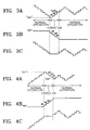
- Figure 3 describes the operation of the first and second up/down counters 106 and 109 and a control voltage applied to the current amplifier 112 for driving the laser diode 101, when the luminous efficiency of the laser diode 101 rises.
- Figure 4 describes the operation of the first and second up/down counters 106 and 109 and the control voltage applied to the current amplifier 112 for driving the laser diode 101, when the luminous efficiency of the laser diode 101 falls.
- the second up/down counter 109 When the first up/down counter 106 overflows ("FF"), namely, when the temperature of the laser diode 101 rises and the luminous efficiency falls, the second up/down counter 109 performs up counting as "81, 82, 83, ! from the offset value ("80") as shown in Figure 4B. At the same time, the first up/down counter 106 performs down counting as "FE, FD, FC, ! as shown in Figure 4A. When the count value of the first up/down counter 106 reaches "80", the second up/down counter 109 stops up counting. Only the first up/down counter 106 continuously operates for stabilizing the luminous efficiency of the laser diode 101.
- the range of the control voltage is extended and the control error is reduced, due to the addition of the second up/down counter 109, the detector 108, and the second digital-to-analog converter 110.
- Embodiments of the present invention can be constructed using various bit resolutions. However, an eight bit structure is preferable, considering manufacturing costs.
Landscapes
- Physics & Mathematics (AREA)
- Optics & Photonics (AREA)
- Electromagnetism (AREA)
- Engineering & Computer Science (AREA)
- Plasma & Fusion (AREA)
- Semiconductor Lasers (AREA)
Claims (6)
- Temperaturkompensationsvorrichtung einer Laserdiode (101) zum Steuern der Ausgangsleitung einer Laserdiode (101) entsprechend der Änderung einer Temperatur, die umfasst:eine erste Erzeugungseinrichtung (104-107), die eine Fehlerspannung zwischen einer Spannung, die der Ausgangsleistung der Laserdiode (101) entspricht, und einer Bezugsspannung erzeugt, wobei die erste Erzeugungseinrichtung umfasst:einen Komparator (104), der die Spannung, die der Ausgangsleistung der Laserdiode (101) entspricht, mit der Bezugsspannung (105) vergleicht und die Fehlerspannung erzeugt, sowie einen ersten Zähler (106), der in Reaktion auf ein Erfassungssignal die Fehlerspannung zählt, die korrigierte Fehlerspannung als einen ersten Zählwert auf Basis der Ausgangsleistung erzeugt und Aufwärts- sowie Abwärtszählen durchführt, um die Fehlerspannung zu ändern; undeine zweite Erzeugungseinrichtung (108-110), die eine korrigierte Steuerspannung durch Empfangen der Fehlerspannung auf Basis der Ausgangsleistung erzeugt und die korrigierte Steuerspannung über einen vorgegebenen Zeitraum an die Laserdiode (101) ausgibt, wobei die zweite Erzeugungseinrichtung umfasst:einen Detektor (108), der Überlauf und Unterlauf des ersten Zählwertes erfasst und das Erfassungssignal erzeugt, einen zweiten Zähler (109), der Abwärts- und Aufwärtszählen in Reaktion auf das Erfassungssignal in umgekehrter Reihenfolge zu dem ersten Zähler (106) durchführt, und eine Einrichtung (111, 112) zum Erzeugen einer Steuerspannung, die die korrigierte Steuerspannung auf Basis der korrigierten Fehlerspannung erzeugt und die korrigierte Steuerspannung erzeugt, die ermittelt wird, indem der Ausgang des ersten Zählers (106) zu dem Ausgang des zweiten Zählers (110) addiert wird, wenn der erste Zählwert überläuft und unterläuft; wobei:der vorgegebene Zeitraum endet, wenn der Pegel der Fehlerspannung ein vorgegebener Kompensationswert wird;der erste Zähler (106) in Reaktion auf das Erfassungssignal Aufwärtszählen bis zu einem vorgegebenen Kompensationswert durchführt, wenn der erste Zählwert unterläuft, und Abwärtszählen bis zu dem Kompensationswert durchführt, wenn der erste Zählwert überläuft;der zweite Zähler (109) Abwärtszählen von einem ersten Wert durchführt, bis der Ausgang des ersten Zählers (106) der Kompensationswert wird, und dann den abwärts gezählten Wert des zweiten Zählers (109) auf den ersten Wert erneuert, wenn der erste Zählwert unterläuft, und Aufwärtszählen von einem zweiten Wert durchführt, bis der Ausgang des ersten Zählers (106) der Kompensationswert wird, und dann den aufwärts gezählten Wert des ersten Zählers (106) auf den zweiten Wert erneuert, wenn der erste Zählwert überläuft;und der Anfangswert des ersten Wertes sowie des zweiten Wertes auf den Kompensationswert eingestellt ist.
- Temperaturkompensationsvorrichtung nach Anspruch 1, wobei:der erste und der zweite Zähler (106, 109) ein erster und ein zweiter Aufwärts-/Abwärts-Zähler sind und der zweite Aufwärts-/Abwärts-Zähler (109) so eingerichtet ist, dass er entsprechend dem Erfassungssignal Aufwärts- und Abwärtszählen durchführt, und so eingerichtet ist, dass er in der umgekehrten Reihenfolge zu dem ersten Aufwärts-/Abwärts-Zähler (106) zählt; unddie Einrichtung zum Erzeugen der Steuerspannung umfasst:einen Addierer (111) sowie einen Stromwandler (112), wobei der Addierer (111) so eingerichtet ist, dass er die Steuerspannung auf Basis der korrigierten Fehlerspannung erzeugt und die gleichmäßige Steuerspannung, die ermittelt wird, indem der Ausgang des ersten Aufwärts-/Abwärts-Zählers (106) zu dem des zweiten Aufwärts-/Abwärts-Zählers (110) addiert wird, an den Stromwandler (112) anlegt, wenn der erste Zählwert überläuft und unterläuft.
- Vorrichtung nach Anspruch 2, wobei der erste Aufwärts-/Abwärts-Zähler (106) Aufwärtszählen bis zu einem vorgegebenen Kompensationswert durchführt, wenn der erste Zählwert unterläuft, und Abwärtszählen bis zu dem Kompensationswert durchführt, wenn der erste Zählwert überläuft.
- Vorrichtung nach Anspruch 3, wobei der zweite Aufwärts-/Abwärts-Zähler (109) entsprechend dem Erfassungssignal Abwärtszählen von einem ersten Wert durchführt, bis der Ausgang des ersten Aufwärts-/Abwärts-Zählers (106) der Kompensationswert wird, und dann den abwärts gezählten Wert des zweiten Aufwärts/Abwärts-Zählers (109) auf den ersten Wert erneuert, wenn der erste Zählwert unterläuft, und Aufwärtszählen von einem zweiten Wert durchführt, bis der Ausgang des ersten Aufwärts-/Abwärts-Zählers (106) der Kompensationswert wird, und dann den aufwärts gezählten Wert des ersten Aufwärts-/Abwärts-Zählers (106) auf den zweiten Wert erneuert, wenn der erste Zählwert überläuft.
- Vorrichtung nach Anspruch 4, wobei der Anfangswert des ersten Wertes und des zweiten Wertes auf den Kompensationswert eingestellt ist.
- Temperaturkompensationsverfahren einer Laserdiode zum Steuern der Ausgangsleistung einer Laserdiode (101) entsprechend einer Temperaturänderung, das die folgenden Schritte umfasst:wobei der Schritt (b) des Weiteren die folgenden Teilschritte umfasst:a) Erzeugen einer Fehlerspannung zwischen einer Spannung, die der Ausgangsleistung der Laserdiode entspricht, und einer Bezugsspannung; undb) Erzeugen einer Steuerspannung durch Korrigieren der Fehlerspannung auf Basis der Ausgangsleistung und Ausdehnen des Bereiches einer Steuerspannung durch Ausgeben einer korrigierten Steuerspannung an die Laserdiode über einen vorgegebenen Zeitraum, wenn der Pegel der Fehlerspannung überläuft oder unterläuft;b1) entsprechend einem Erfassungssignal Zählen der Fehlerspannung, Erzeugen eines ersten Zählwertes, der der korrigierten Fehlerspannung auf Basis der Ausgangsleistung entspricht, und Aufwärts- sowie Abwärtszählen des ersten Zählwertes, um die korrigierte Fehlerspannung zu ändern;b2) Erfassen, ob der erste Zählwert überläuft oder unterläuft und Erzeugen des Erfassungssignals;b3) Durchführen von Abwärts- und Aufwärtszählen entsprechend dem Erfassungssignal in der zu dem ersten Zählschritt in Schritt b1) umgekehrten Reihenfolge und Erzeugen eines zweiten Zählwertes; undb4) Erzeugen einer Steuerspannung auf Basis der korrigierten Fehlerspannung und Erzeugen einer gleichmäßigen Steuerspannung, die ermittelt wird, indem der erste Zählwert zu dem zweiten Zählwert addiert wird, wenn der erste Zählwert überläuft oder unterläuft, wobei entsprechend dem Erfassungssignal in dem Schritt b1) Aufwärtszählen bis zu einem vorgegebenen Kompensationswert entsprechend dem Erfassungssignal durchgeführt wird, wenn der erste Zählwert unterläuft, und Abwärtszählen bis zu dem Kompensationswert durchgeführt wird, wenn der erste Zählwert überläuft, und in dem Schritt b3) Abwärtszählen von einem ersten Wert durchgeführt wird, bis der erste Zählwert der Kompensationswert wird, und dann der abwärts gezählte Wert auf den ersten Wert erneuert wird, wenn der erste Zählwert unterläuft, und Aufwärtszählen von einem zweiten vorgegebenen Wert durchgeführt wird, bis der erste Zählwert der Kompensationswert wird, und dann der aufwärts gezählte Wert auf den zweiten Wert erneuert wird, wenn der erste Zählwert überläuft.
Applications Claiming Priority (2)
| Application Number | Priority Date | Filing Date | Title |
|---|---|---|---|
| KR9768345 | 1997-12-12 | ||
| KR1019970068345A KR100252103B1 (ko) | 1997-12-12 | 1997-12-12 | 레이저 다이오드의 온도 보상 장치 및 방법 |
Publications (2)
| Publication Number | Publication Date |
|---|---|
| EP0923174A1 EP0923174A1 (de) | 1999-06-16 |
| EP0923174B1 true EP0923174B1 (de) | 2004-11-24 |
Family
ID=19527216
Family Applications (1)
| Application Number | Title | Priority Date | Filing Date |
|---|---|---|---|
| EP98304406A Expired - Lifetime EP0923174B1 (de) | 1997-12-12 | 1998-06-04 | Vorrichtung und Verfahren zur Temperaturkompensation von Laserdioden |
Country Status (6)
| Country | Link |
|---|---|
| US (2) | US6324198B1 (de) |
| EP (1) | EP0923174B1 (de) |
| JP (1) | JP3034496B2 (de) |
| KR (1) | KR100252103B1 (de) |
| CN (1) | CN1123103C (de) |
| DE (1) | DE69827748T2 (de) |
Families Citing this family (18)
| Publication number | Priority date | Publication date | Assignee | Title |
|---|---|---|---|---|
| KR100346701B1 (ko) * | 1999-05-25 | 2002-08-01 | 삼성전자 주식회사 | 레이저 다이오드의 출력 제어 방법 및 이에 적합한 장치 |
| US20030174744A1 (en) * | 2002-03-13 | 2003-09-18 | Reilly Timothy J. | Digital control of burst mode laser |
| US6922423B2 (en) * | 2003-04-11 | 2005-07-26 | Robert L. Thornton | Control system for a semiconductor laser |
| US7650077B2 (en) * | 2005-10-25 | 2010-01-19 | Source Photonics Santa Clara, Inc. | Multi-data-rate optical transceiver |
| US20050135756A1 (en) * | 2003-12-19 | 2005-06-23 | Chao Zhang | Bi-directional optical transceiver module having automatic-restoring unlocking mechanism |
| US7183540B2 (en) * | 2005-03-17 | 2007-02-27 | Fiberxon Inc. | Apparatus for measuring photo diodes' temperature dependence |
| US8036539B2 (en) * | 2005-06-28 | 2011-10-11 | Finisar Corporation | Gigabit ethernet longwave optical transceiver module having amplified bias current |
| CN100414618C (zh) * | 2005-08-15 | 2008-08-27 | 上海乐金广电电子有限公司 | 光记录装置内写入功率控制装置及其控制方法 |
| US7153043B1 (en) | 2006-01-19 | 2006-12-26 | Fiberxon, Inc. | Optical transceiver having improved printed circuit board |
| JP2007294747A (ja) * | 2006-04-26 | 2007-11-08 | Matsushita Electric Ind Co Ltd | レーザ駆動回路、レーザ駆動方法、記録再生装置 |
| US7507037B2 (en) * | 2006-11-27 | 2009-03-24 | Fiberxon, Inc. | Optical transceiver having improved unlocking mechanism |
| USD594455S1 (en) | 2006-11-27 | 2009-06-16 | Source Photonics Santa Clara, Inc. | Removable key to be used to unlock an optical transceiver module |
| WO2015175178A1 (en) * | 2014-05-15 | 2015-11-19 | Seagate Technology Llc | Controlling laser output in a hamr device |
| US9355671B2 (en) | 2014-05-15 | 2016-05-31 | Seagate Technology Llc | Controlling laser output in a HAMR device |
| US9153272B1 (en) | 2014-05-15 | 2015-10-06 | Seagate Technology Llc | Characterizing laser output in a HAMR device |
| CN104538831B (zh) * | 2014-12-15 | 2018-05-15 | 北京航天易联科技发展有限公司 | 一种分布式反馈激光器温度补偿装置 |
| US9236081B1 (en) * | 2015-03-31 | 2016-01-12 | Seagate Technology Llc | Laser temperature calibration in a HAMR device |
| CN112213277A (zh) * | 2020-09-29 | 2021-01-12 | 湖北鑫英泰系统技术股份有限公司 | 油浸式设备油路控制方法及装置 |
Family Cites Families (11)
| Publication number | Priority date | Publication date | Assignee | Title |
|---|---|---|---|---|
| JPS561923A (en) * | 1979-06-20 | 1981-01-10 | Dainippon Screen Mfg Co Ltd | Stabilizing method for quantity of light in optical system using light deflecting element |
| JPS57162481A (en) * | 1981-03-23 | 1982-10-06 | Ibm | Control circuit for light emtting semiconductor device |
| JP2503202B2 (ja) * | 1985-01-30 | 1996-06-05 | 株式会社リコー | 半導体レ−ザの出力制御装置 |
| JPH0614663B2 (ja) * | 1986-09-19 | 1994-02-23 | 株式会社リコー | 光走査装置 |
| JPS6382020A (ja) | 1986-09-25 | 1988-04-12 | Matsushita Electric Works Ltd | 比較機能付き計数回路 |
| US4856008A (en) * | 1987-12-29 | 1989-08-08 | Ricoh Company, Ltd. | Semiconductor laser control apparatus |
| JPH0635998B2 (ja) | 1988-06-01 | 1994-05-11 | 日本電気株式会社 | キャプチャ装置 |
| JP2815183B2 (ja) * | 1989-08-01 | 1998-10-27 | 株式会社リコー | レーザビーム走査位置検知装置 |
| JPH04260268A (ja) * | 1991-02-15 | 1992-09-16 | Brother Ind Ltd | 半導体レーザ駆動装置 |
| JP3182167B2 (ja) | 1991-07-04 | 2001-07-03 | 三洋電機株式会社 | レーザー駆動回路 |
| JP3648302B2 (ja) * | 1995-11-13 | 2005-05-18 | リコー光学株式会社 | 半導体レーザ駆動装置 |
-
1997
- 1997-12-12 KR KR1019970068345A patent/KR100252103B1/ko not_active Expired - Fee Related
-
1998
- 1998-05-19 JP JP10137274A patent/JP3034496B2/ja not_active Expired - Fee Related
- 1998-06-04 DE DE69827748T patent/DE69827748T2/de not_active Expired - Fee Related
- 1998-06-04 EP EP98304406A patent/EP0923174B1/de not_active Expired - Lifetime
- 1998-06-12 CN CN98114806A patent/CN1123103C/zh not_active Expired - Fee Related
- 1998-06-16 US US09/099,066 patent/US6324198B1/en not_active Expired - Fee Related
-
2001
- 2001-07-13 US US09/903,529 patent/US6741622B2/en not_active Expired - Fee Related
Also Published As
| Publication number | Publication date |
|---|---|
| CN1219738A (zh) | 1999-06-16 |
| JP3034496B2 (ja) | 2000-04-17 |
| DE69827748T2 (de) | 2005-05-12 |
| EP0923174A1 (de) | 1999-06-16 |
| KR100252103B1 (ko) | 2000-05-01 |
| US6741622B2 (en) | 2004-05-25 |
| US20010048696A1 (en) | 2001-12-06 |
| US6324198B1 (en) | 2001-11-27 |
| KR19990049406A (ko) | 1999-07-05 |
| CN1123103C (zh) | 2003-10-01 |
| JPH11186644A (ja) | 1999-07-09 |
| DE69827748D1 (de) | 2004-12-30 |
Similar Documents
| Publication | Publication Date | Title |
|---|---|---|
| EP0923174A1 (de) | Vorrichtung und Verfahren zur Temperaturkompensation von Laserdioden | |
| US5414280A (en) | Current driven voltage sensed laser drive (CDVS LDD) | |
| KR960005410B1 (ko) | 디지탈 서보 회로 | |
| EP0539038A2 (de) | Optische Sender | |
| EP1187275A2 (de) | Verfahren und Vorrichtung zur Verstärkungsregelung für Erbium-dotierten Faserverstärker | |
| JP2001053377A (ja) | 半導体レーザ駆動装置 | |
| JPH07141677A (ja) | 半導体レーザの駆動装置 | |
| JPH11205248A (ja) | 光送信器 | |
| KR0153066B1 (ko) | 반도체 레이저 장치, 정보기록 및 재생장치와 이미지 기록장치 | |
| US4853934A (en) | Semiconductor laser control apparatus | |
| US7680166B2 (en) | Laser drive, optical disc apparatus, and laser-driving method | |
| US6151339A (en) | Thermal compensation of injection laser diodes driven by shunt current modulators | |
| KR100498444B1 (ko) | 디스크 드라이브의 레이저 파워 제어 장치 및 방법 | |
| EP1231602B1 (de) | Automatische Leistungsregelung für einen optischen Plattenspieler | |
| US5506853A (en) | Offset stabilization of wide dynamic range injection laser diode with single bit sampling | |
| US5046158A (en) | Optical scanning apparatus with control circuit for optimizing the operating range of an A/D converter | |
| JP3323033B2 (ja) | 半導体レーザ制御装置、半導体レーザ装置、情報記録再生装置及び画像記録装置 | |
| JP2910350B2 (ja) | 光メモリ装置及びそのサーボオフセット補正方法 | |
| JP2888989B2 (ja) | レーザーダイオードの光出力制御のための方法および回路装置 | |
| JP3109467B2 (ja) | 光送信器 | |
| JPH11144285A (ja) | 半導体レーザ駆動装置及びそれを用いた光ディスク装置 | |
| JP3743399B2 (ja) | レーザダイオード制御装置、及び制御方法 | |
| JP3961883B2 (ja) | 情報記録装置 | |
| JPH08147746A (ja) | 光学式情報記録再生装置 | |
| JPH01206366A (ja) | 半導体レーザー出力制御装置 |
Legal Events
| Date | Code | Title | Description |
|---|---|---|---|
| PUAI | Public reference made under article 153(3) epc to a published international application that has entered the european phase |
Free format text: ORIGINAL CODE: 0009012 |
|
| 17P | Request for examination filed |
Effective date: 19980617 |
|
| AK | Designated contracting states |
Kind code of ref document: A1 Designated state(s): DE GB NL |
|
| AX | Request for extension of the european patent |
Free format text: AL;LT;LV;MK;RO;SI |
|
| 17Q | First examination report despatched |
Effective date: 20000111 |
|
| AKX | Designation fees paid |
Free format text: DE GB NL |
|
| GRAP | Despatch of communication of intention to grant a patent |
Free format text: ORIGINAL CODE: EPIDOSNIGR1 |
|
| RIC1 | Information provided on ipc code assigned before grant |
Ipc: 7G 11B 7/125 B Ipc: 7H 01S 5/068 A |
|
| RIC1 | Information provided on ipc code assigned before grant |
Ipc: 7G 11B 7/125 B Ipc: 7H 01S 5/068 A |
|
| GRAS | Grant fee paid |
Free format text: ORIGINAL CODE: EPIDOSNIGR3 |
|
| GRAA | (expected) grant |
Free format text: ORIGINAL CODE: 0009210 |
|
| AK | Designated contracting states |
Kind code of ref document: B1 Designated state(s): DE GB NL |
|
| REG | Reference to a national code |
Ref country code: GB Ref legal event code: FG4D |
|
| REF | Corresponds to: |
Ref document number: 69827748 Country of ref document: DE Date of ref document: 20041230 Kind code of ref document: P |
|
| PLBE | No opposition filed within time limit |
Free format text: ORIGINAL CODE: 0009261 |
|
| STAA | Information on the status of an ep patent application or granted ep patent |
Free format text: STATUS: NO OPPOSITION FILED WITHIN TIME LIMIT |
|
| 26N | No opposition filed |
Effective date: 20050825 |
|
| PGFP | Annual fee paid to national office [announced via postgrant information from national office to epo] |
Ref country code: NL Payment date: 20080603 Year of fee payment: 11 Ref country code: DE Payment date: 20080612 Year of fee payment: 11 |
|
| PGFP | Annual fee paid to national office [announced via postgrant information from national office to epo] |
Ref country code: GB Payment date: 20080604 Year of fee payment: 11 |
|
| GBPC | Gb: european patent ceased through non-payment of renewal fee |
Effective date: 20090604 |
|
| NLV4 | Nl: lapsed or anulled due to non-payment of the annual fee |
Effective date: 20100101 |
|
| PG25 | Lapsed in a contracting state [announced via postgrant information from national office to epo] |
Ref country code: GB Free format text: LAPSE BECAUSE OF NON-PAYMENT OF DUE FEES Effective date: 20090604 |
|
| PG25 | Lapsed in a contracting state [announced via postgrant information from national office to epo] |
Ref country code: DE Free format text: LAPSE BECAUSE OF NON-PAYMENT OF DUE FEES Effective date: 20100101 |
|
| PG25 | Lapsed in a contracting state [announced via postgrant information from national office to epo] |
Ref country code: NL Free format text: LAPSE BECAUSE OF NON-PAYMENT OF DUE FEES Effective date: 20100101 |