EP0920162A2 - Verfahren und Anordnung zur Korrektur des Phasenfehlers eines PSK-signals - Google Patents
Verfahren und Anordnung zur Korrektur des Phasenfehlers eines PSK-signals Download PDFInfo
- Publication number
- EP0920162A2 EP0920162A2 EP98250418A EP98250418A EP0920162A2 EP 0920162 A2 EP0920162 A2 EP 0920162A2 EP 98250418 A EP98250418 A EP 98250418A EP 98250418 A EP98250418 A EP 98250418A EP 0920162 A2 EP0920162 A2 EP 0920162A2
- Authority
- EP
- European Patent Office
- Prior art keywords
- signal
- phase
- error
- inphase
- quadrature
- Prior art date
- Legal status (The legal status is an assumption and is not a legal conclusion. Google has not performed a legal analysis and makes no representation as to the accuracy of the status listed.)
- Withdrawn
Links
- 238000000034 method Methods 0.000 title claims abstract description 23
- 238000013507 mapping Methods 0.000 claims description 29
- 230000035945 sensitivity Effects 0.000 description 10
- 238000010586 diagram Methods 0.000 description 9
- 238000010276 construction Methods 0.000 description 8
- 238000001514 detection method Methods 0.000 description 7
- 238000012545 processing Methods 0.000 description 7
- 230000006870 function Effects 0.000 description 4
- 230000010363 phase shift Effects 0.000 description 4
- 238000004891 communication Methods 0.000 description 2
- 239000000470 constituent Substances 0.000 description 1
- 230000000694 effects Effects 0.000 description 1
- 238000012986 modification Methods 0.000 description 1
- 230000004048 modification Effects 0.000 description 1
Images


Classifications
-
- H—ELECTRICITY
- H04—ELECTRIC COMMUNICATION TECHNIQUE
- H04L—TRANSMISSION OF DIGITAL INFORMATION, e.g. TELEGRAPHIC COMMUNICATION
- H04L27/00—Modulated-carrier systems
- H04L27/18—Phase-modulated carrier systems, i.e. using phase-shift keying
- H04L27/22—Demodulator circuits; Receiver circuits
- H04L27/227—Demodulator circuits; Receiver circuits using coherent demodulation
- H04L27/2271—Demodulator circuits; Receiver circuits using coherent demodulation wherein the carrier recovery circuit uses only the demodulated signals
- H04L27/2273—Demodulator circuits; Receiver circuits using coherent demodulation wherein the carrier recovery circuit uses only the demodulated signals associated with quadrature demodulation, e.g. Costas loop
-
- H—ELECTRICITY
- H04—ELECTRIC COMMUNICATION TECHNIQUE
- H04L—TRANSMISSION OF DIGITAL INFORMATION, e.g. TELEGRAPHIC COMMUNICATION
- H04L27/00—Modulated-carrier systems
- H04L27/0014—Carrier regulation
- H04L2027/0024—Carrier regulation at the receiver end
- H04L2027/0026—Correction of carrier offset
- H04L2027/003—Correction of carrier offset at baseband only
-
- H—ELECTRICITY
- H04—ELECTRIC COMMUNICATION TECHNIQUE
- H04L—TRANSMISSION OF DIGITAL INFORMATION, e.g. TELEGRAPHIC COMMUNICATION
- H04L27/00—Modulated-carrier systems
- H04L27/0014—Carrier regulation
- H04L2027/0044—Control loops for carrier regulation
- H04L2027/0053—Closed loops
- H04L2027/0057—Closed loops quadrature phase
-
- H—ELECTRICITY
- H04—ELECTRIC COMMUNICATION TECHNIQUE
- H04L—TRANSMISSION OF DIGITAL INFORMATION, e.g. TELEGRAPHIC COMMUNICATION
- H04L27/00—Modulated-carrier systems
- H04L27/0014—Carrier regulation
- H04L2027/0044—Control loops for carrier regulation
- H04L2027/0063—Elements of loops
- H04L2027/0067—Phase error detectors
Definitions
- the present invention relates to an error detecting method and device for detecting a phase error in a PSK modulated signal, and a signal demodulating method and device for demodulating a PSK modulated signal.
- a PSK (phase shift keying) system is known as one modulating means in the case of transmitting a digital signal.
- a binary value of a digital signal is expressed by a phase of a modulated signal. For example, if the modulation phase number is 2 M , a digital signal of M bits can be transmitted at once.
- an inphase signal and a quadrature signal are generated from a received modulated signal, a phase difference between a received phase of the modulated signal and a reference phase is detected on the basis of the inphase signal and the quadrature signal, and then, the detected phase difference is fed back to synchronously demodulate the inphase signal and the quadrature signal.
- the received phase of the modulated signal is mapped by allocating the inphase signal and the quadrature signal as values of the axis of abscissas and the axis of ordinates in a complex plane, and an interior angle ⁇ between a pair of lines one passing from the origin to the received phase and other passing from the origin to the reference phase, is calculated.
- reference phases of a 8-phase modulated signal are plotted in the complex plane.
- a specific procedure for detecting the phase difference of the modulated signal on the basis of the inphase signal and the quadrature signal as mentioned above includes for example use of a previously prepared table. Namely, phase errors previously calculated from ⁇ tan -1 ⁇ is set in a table addressed with the inphase signal and the quadrature signal, and the table thus completed is stored in an information storing medium such as a ROM (read only memory).
- the error detecting device becomes too large.
- it may be considered to calculate, in real time, the phase difference or phase error from the inphase signal and the quadrature signal without using the above mentioned table.
- the device for executing this calculation is disclosed in for example "Fundamentals and Applications of Digital PLL", (Japanese language book) page 93, Trikeppuse EX11.
- This book shows a simple circuit for approximately calculating the phase error from the inphase signal and the quadrature signal, and therefore, if this circuit is used, it is possible to remarkably reduce the circuit scale of the error detecting device.
- the PSK modulated signal a digital broadcasting in order to transmit a high quality image data.
- it is also considered to sequentially transmit in a time sharing manner, a plurality of kinds of PSK modulated signals having different modulation phase numbers, as shown in Fig. 10.
- a signal demodulating device when modulated signals of two phases to 8 phases (binary phase shift keying (BPSK), quadrature phase shift keying (QPSK), and octal phase shift keying (OPSK or 8PSK) are transmitted in a time division as shown in Fig. 10, if the image data is transmitted by the modulated signals of QPSK and 8PSK, a signal demodulating device can reproduce a high quality image data from the modulated signals of 8PSK if a communication condition is good, and also can reproduce a low quality image data from the modulated signals of QPSK if the communication condition is bad. Furthermore, it is also considered to make the timing division ratio of the QPSK modulated signal and the 8PSK modulated signal variable, and to transmit the timing division ratio by the BPSK modulated signal.
- BPSK binary phase shift keying
- QPSK quadrature phase shift keying
- OPSK or 8PSK octal phase shift keying
- the error detecting device is also required to detect the phase error in the plurality of kinds of PSK modulated signals.
- the circuit disclosed by the above referred book for detecting the phase error is different between the binary phase and the quadrature phase
- the phase error device capable of complying with both the binary phase and the quadrature phase is constructed by using the circuit disclosed by the above referred book, it is sufficient if a circuit for the binary phase and anther circuit the quadrature phase are constructed separately from each other, and are connected in parallel to a selector circuit.
- phase error detecting circuits are provided for different phase numbers, respectively and are connected in parallel to the selector circuit, it is possible to detect the phase error of the plurality of kinds of modulated signals having different modulation phase numbers.
- a phase error calculating method is different from the binary phase to the quadrature phase, a phase error detecting sensitivity becomes different from the binary phase to the quadrature phase.
- the phase error is approximately calculated by multiplying a quadrature signal Q by a positive/negative sign of an inphase signal I.
- the phase error is approximately calculated by subtracting the value obtained by multiplying the quadrature signal Q by a positive/negative sign of the inphase signal I, from the value obtained by multiplying the inphase signal I by a positive/negative sign of the quadrature signal Q
- the reference positions of the binary phase can assume two different conditions, in one of which the reference positions are positioned on the axis of abscissas in the complex plane as shown in Fig. 12A, and in the other of which the reference positions are positioned on the axis of ordinates in the complex plane as shown in Fig. 12C.
- the phase error detecting method is different from each other, and therefore, the one phase difference detecting circuit as mentioned above for the binary phase can no longer comply with.
- the reference position patterns of the quadrature phase in the complex phase becomes two as shown in Figs. 11A and 11B, and the reference position patterns of the binary phase in the complex phase becomes four as shown in Figs. 12A, 12B, 12C and 12D. Therefore, it becomes difficult to detect the phase error with an appropriate sensitivity.
- Another object of the present invention is to provide an error detecting method and device, capable of appropriately detecting the phase error when the modulation phase number changes, without requiring a large scale circuit.
- Still another object of the present invention is to provide a signal demodulating method and device capable of demodulating a modulated signal having a changing modulation phase number, without requiring a large scale circuit.
- an error detecting method for calculating a phase error in a PSK modulated signal having a predetermined modulation phase number, and so configured that a received phase of the modulated signal is mapped on a complex plane by allocating an inphase signal and a quadrature signal generated from the modulated signal as values of the axis of abscissas and the axis of ordinates, and a phase error between the received phase of the modulated signal thus mapped and a reference phase in each of a plurality of signal areas, the method including the steps of:
- the received phase is mapped to the complex plane divided into eight signal areas, and the distance between one mapped position and eight reference straight lines are calculated as eight phase errors.
- one signal area to which the received phase is mapped is discriminated and selected from the eight signal areas, and one phase error corresponding to the discriminated signal area is selected from the eight phase errors. Since this phase error is approximately calculated as the distance between the mapped position and the reference straight line, the calculation of the phase error can be simply and easily processed.
- the reference phase means a phase becoming the reference for calculating the phase error from the modulated signal.
- the modulation phase number is eight phases
- eight reference phases are set which are obtained by rotating by each 45° from a position of 0°.
- the reference straight line means a straight line passing from the origin through the reference phase on the complex plane.
- the modulation phase number is eight phases
- the "signal areas” means areas obtained by equally dividing the complex plane by the modulation phase number in such a manner that each reference straight line is positioned at an angular center line of a corresponding signal area.
- the modulation phase number is eight phases, there are eight signal areas each having an interior angle of 45°, in such a manner that a first signal area is extended in the range of -22.5° to +22.5°, a second signal area is extended in the range of +22.5° to +67.5°, and so on.
- an error detecting method for calculating a phase error in a PSK modulated signal having a modulation phase number changing in a time division manner, and so configured that a received phase of the modulated signal is mapped on a complex plane by allocating an inphase signal and a quadrature signal generated from the modulated signal as values of the axis of abscissas and the axis of ordinates, and a phase error between the received phase of the modulated signal thus mapped and a reference phase in each of a plurality of signal areas, the method including the steps of:
- the received phase is mapped to the complex plane divided into four signal areas corresponding to the modulation phase number, and eight phase errors are individually calculated between the one mapped position and the eight reference straight lines corresponding to the maximum modulation phase number.
- one signal area to which the received phase is mapped is selected from the four signal areas, and one phase error corresponding to the selected signal area is selected from the eight phase errors, so that one appropriate phase error of the modulated signal can be outputted.
- the phase error thus outputted corresponds to the reference phase of the maximum modulation phase number, and is the same even if the modulation phase number of the modulated signal changes. Therefore, the detection sensitivity of the phase error does not vary even if the modulation phase number of the modulated signal changes in the time division manner.
- an error detecting device for calculating a phase error in a PSK modulated signal having a predetermined modulation phase number, and so configured that a received phase of the modulated signal is mapped on a complex plane by allocating an inphase signal and a quadrature signal generated from the modulated signal as values of the axis of abscissas and the axis of ordinates, and a phase error between the received phase of the modulated signal thus mapped and a reference phase in each of a plurality of signal areas, the device including:
- the received phase is mapped to the complex plane divided into eight signal areas, and the distance between one mapped position and eight reference straight lines are calculated as eight phase errors.
- one signal area to which the received phase is mapped is discriminated and selected from the eight signal areas, and one phase error corresponding to the discriminated signal area is selected from the eight phase errors. Since this phase error is approximately calculated as the distance between the mapped position and the reference straight line, the calculation of the phase error can be simply and easily processed. Therefore, the error detecting device can be realized in a small scale circuit having a simple construction.
- various means included in the error detecting device can be constituted of any means if a necessary function is realized.
- the various means can be constituted of a dedicated hardware, or alternatively, can be realized by a computer installed with a program for the necessary function, or a function internally realized in a computer by an appropriate program, or may be a combination of these means.
- an error detecting device for calculating a phase error in a PSK modulated signal having a modulation phase number changing in a time division manner, and so configured that a received phase of the modulated signal is mapped on a complex plane by allocating an inphase signal and a quadrature signal generated from the modulated signal as values of the axis of abscissas and the axis of ordinates, and a phase error between the received phase of the modulated signal thus mapped and a reference phase in each of a plurality of signal areas, the device including:
- the received phase is mapped to the complex plane divided into four signal areas corresponding to the modulation phase number, and eight phase errors are individually calculated between the one mapped position and the eight reference straight lines corresponding to the maximum modulation phase number.
- one signal area to which the received phase is mapped is selected from the four signal areas, and one phase error corresponding to the selected signal area is selected from the eight phase errors, so that one appropriate phase error of the modulated signal can be outputted.
- the phase error thus outputted corresponds to the reference phase of the maximum modulation phase number, and is the same even if the modulation phase number of the modulated signal changes. Therefore, the detection sensitivity of the phase error does not vary even if the modulation phase number of the modulated signal changes in the time division manner.
- the error calculating means calculates the phase error between the received phase of the modulated signal mapped by the signal mapping means and a reference phase in each of the plurality of signal areas corresponding to the maximum modulation phase number, as a distance between the mapped position of the modulated signal and a reference straight line, from at least one of the inphase signal and the quadrature signal, so as to obtain a plurality of phase errors.
- the error detecting device can be constituted of a small scale circuit having a simple construction.
- the error calculating means calculates the phase error between eight reference phases and the modulated signal, as "Q ⁇ 2", “-I+Q”, “-I ⁇ 2", “-I-Q”, “-Q ⁇ 2”, “I-Q”, “I ⁇ 2” and “I+Q”, the inphase signal I and the quadrature signal Q.
- the phase error of the octal phase PSK modulated signal can be calculated as the distance between the mapped position and the reference straight lines, and therefore, the circuit for calculating the phase error can be reduced in circuit scale.
- the error calculating means calculates the phase error between eight reference phases and the modulated signal, as "Q ⁇ 2", “-I+Q”, “-I ⁇ 2", “-I-Q”, “-Q ⁇ 2”, “I-Q”, “I ⁇ 2” and “I+Q”, the inphase signal I and the quadrature signal Q.
- the phase error of the modulated signal having the modulation phase number changing m the time division manner can be calculated as the distance between the mapped position and the reference straight lines, and therefore, the detection sensitivity of the phase error does not vary even if the modulation phase number of the modulated signal changes.
- the error calculating means calculates only one of a pair of phase errors having the same value and different positive/negative signs, and then, sign-inverts the calculated phase error.
- the error calculating means calculates "Q ⁇ 2", “-I+Q”, “-I ⁇ 2”, “-I-Q”, “-Q ⁇ 2”, “I-Q”, “I ⁇ 2” and “I+Q”, as the phase errors, for example, only one of "Q ⁇ 2" and “-Q ⁇ 2” is calculated, and the calculated phase error is sign-inverted. Similarly, only one of "-I+Q” and “I-Q”, only one of "-I ⁇ 2” and “I ⁇ 2” and only one of "-I-Q” and “I+Q” are calculated, and the respective calculated phase errors are sign-inverted. In this case, the circuit for calculating a number of phase errors can be simplified.
- the above mentioned error calculating means includes four error calculating circuits each calculating only one of a pair of phase errors having the same value and different positive/negative signs, and a positive/negative signs inverting circuit receiving the output of each of the four error calculating circuits for outputting a sign-inverted phase error.
- the eight phase errors can be speedily calculated by a simple circuit.
- the area discriminating means detects one of the "positive/negative sign of the inphase signal I", the “positive/negative sign of the quadrature signal Q", the “positive/negative sign of the sum of the inphase signal I and the quadrature signal Q", and the "positive/negative sign of the result obtained by subtracting one of the inphase signal I and the quadrature signal Q from the other", for the four area patterns, and selects one from the two signal areas.
- the area patterns for the two phases becomes four. From the two signal areas of each of the four area patterns, one signal area to which the received phase is mapped, is selected on the basis of the inphase signal I and the quadrature signal Q. For example, in the area pattern in which the complex plane is divided into a signal area of "0° to 180°” and another signal area of "180° to 0°", one signal area is selected from the two signal areas on the basis of the "positive/negative sign of the quadrature signal Q".
- one signal area is selected from the two signal areas on the basis of the "positive/negative sign of the result obtained by subtracting one of the inphase signal I and the quadrature signal Q from the other".
- one signal area is selected from the two signal areas on the basis of the "positive/negative sign of the inphase signal I".
- one signal area is selected from the two signal areas on the basis of the "positive/negative sign of the sum of the inphase signal I and the quadrature signal Q".
- the necessary phase error signal can be simply and surely obtained from the inphase signal I and the quadrature signal Q.
- the area discriminating means detects one of the "positive and negative combination of the inphase signal I and the quadrature signal Q", and the "positive/negative sign of the result obtained by subtracting one of the inphase signal I and the quadrature signal Q from the other", for the two area patterns, and selects one from the four signal areas.
- the area patterns for the four phases becomes two. From the four signal areas of each of the two area patterns, one signal area to which the received phase is mapped, is selected on the basis of the inphase signal I and the quadrature signal Q. For example, in the area pattern in which the complex plane is divided into four signal areas of "0° to 90°”, “90° to 180°”, “180° to 270°” and “270° to 0°", and another signal area of "180° to 0°", one signal area is selected from the four signal areas on the basis of the "positive and negative combination of the inphase signal I and the quadrature signal Q".
- one signal area is selected from the four signal areas on the basis of the "positive/negative sign of the result obtained by subtracting one of the inphase signal I and the quadrature signal Q from the other".
- the necessary phase error signal can be simply and surely obtained from the inphase signal I and the quadrature signal Q.
- the area discriminating means detects one of the "positive/negative sign of the inphase signal I", the "positive/negative sign of the quadrature signal Q", the "positive/negative sign of the sum of the inphase signal I and the quadrature signal Q", and the "positive/negative sign of the result obtained by subtracting one of the inphase signal I and the quadrature signal Q from the other", for the four area patterns, and selects one from the two signal areas.
- the area discriminating means detects one of the "positive and negative combination of the inphase signal I and the quadrature signal Q", and the "positive/negative sign of the result obtained by subtracting one of the inphase signal I and the quadrature signal Q from the other", for the two area patterns, and selects one from the four signal areas.
- the area discriminating means selects one signal area from each two area patterns for the four phases, causes the error calculating means to calculate the phase error in each of the two area patterns, and selects a smaller one from the two calculated phase errors.
- the area patterns for the two phases becomes four. From the two signal areas of each of the four area patterns, one signal area to which the received phase is mapped, is selected on the basis of the inphase signal I and the quadrature signal Q. The area patterns for the four phases becomes two. From the four signal areas of each of the two area patterns, one signal area to which the received phase is mapped, is selected on the basis of the inphase signal I and the quadrature signal Q. The area pattern for the eight phases is one.
- one signal area to which the received phase is mapped is selected from the eight signal areas, one signal area is selected in each of the two area patterns for the four phases, and a phase error is calculated in each selected signal area, and then, a smaller one is selected from the two phase errors.
- the necessary phase error signal can be simply and surely obtained from the inphase signal I and the quadrature signal Q.
- a signal demodulating method comprising the steps of:
- the phase error of the modulated signal can be calculated as the distance between the mapped position and the reference straight line, and therefore, calculation of the phase error can be easily and simply processed.
- a signal demodulating method comprising the steps of:
- the phase error of the modulated signal corresponds to the reference phase of the maximum modulation phase number, the phase error is the same even if the modulation phase number of the modulated signal changes. Therefore, even if the modulation phase number of the modulated signal changes in the time division manner, the detection sensitivity of the phase error does not vary. Accordingly, the modulated signal having the changing modulation phase number can be appropriately demodulated.
- a signal demodulating device comprising:
- the phase error of the modulated signal can be calculated as the distance between the mapped position and the reference straight line, and therefore, calculation of the phase error can be easily and simply processed. Accordingly, the signal demodulating device can be constituted of a small scale circuit having a simple construction.
- the receiving means receives a PSK modulated signal having different modulation phase numbers sequentially transmitted in a time division manner
- the device further includes a phase number detecting means for detecting the modulation phase numbers sequentially changing in the time division manner, of the modulated signal received by the data receiving means.
- the error calculating means calculates the phase error between the received phase of the modulated signal mapped on the complex plane and a reference phase in each of the plurality of signal areas corresponding to a maximum modulation phase number, from at least one of the inphase signal and the quadrature signal, so as to obtain a plurality of phase errors
- the area discriminating means discriminates the one signal area to which the received phase is mapped, from the plurality of signal areas corresponding to the modulation phase number, on the basis of the inphase signal and the quadrature signal.
- the phase error of the modulated signal corresponds to the reference phase of the maximum modulation phase number
- the phase error is the same even if the modulation phase number of the modulated signal changes. Therefore, even if the modulation phase number of the modulated signal changes in the time division manner, the detection sensitivity of the phase error does not vary. Accordingly, the modulated signal having the changing modulation phase number can be appropriately demodulated.
- the signal demodulating device can be constituted of a small scale circuit having a simple construction.
- a signal demodulating device comprising:
- the phase error of the modulated signal corresponds to the reference phase of the maximum modulation phase number
- the phase error is the same even if the modulation phase number of the modulated signal changes. Therefore, even if the modulation phase number of the modulated signal changes in the time division manner, the detection sensitivity of the phase error does not vary. Accordingly, the modulated signal having the changing modulation phase number can be appropriately demodulated. Furthermore, the signal demodulating device can be constituted of a small scale circuit having a simple construction.
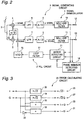
- FIG. 2 there is shown a block diagram illustrating an essential part of an embodiment of the signal demodulating device in accordance with the present invention.
- the shown embodiment of the signal demodulating device in accordance with the present invention includes a radio receiver antenna 2 for receiving a radio signal of the PSK modulated signal.
- this received radio modulated signal is assumed to be a satellite broadcasting of the ISDB (integrated services digital broadcasting) system.
- the modulation phase number cyclically changes in the order of the binary phase, the quadrature phase and the octal phase.
- the antenna 2 is connected to a signal generating circuit 3, which corresponds to a signal generating means, for generating an inphase signal I and a quadrature signal Q from the received modulated signal.
- a signal generating circuit 3 which corresponds to a signal generating means, for generating an inphase signal I and a quadrature signal Q from the received modulated signal.
- an internal construction of the signal generating circuit 3 is divided into two signal processing systems, one of which includes a multiplier 4, a low pass filter 6, an A/D (analog to digital) converter 8, a roll-off filter 10 and a signal output terminal 12 cascade-connected in the named order, and the other of which includes a multiplier 5, a low pass filter 7, an A/D converter 9, a roll-off filter 11 and a signal output terminal 13 cascade-connected in the named order,
- the signal output terminals 12 and 13 are connected to a pair of signal input terminals of an error detecting circuit 21, which is one error detecting means.
- One signal output terminal of this error detecting circuit 21 is connected through a loop filter 14 to a voltage controlled oscillator (VCO) 15.
- VCO voltage controlled oscillator
- An output of this voltage controlled oscillator is connected directly to the multiplier 4 for the inphase signal I, and also connected through a ⁇ /2 phase shifter 16 to the multiplier 5 for the quadrature signal Q.
- the error detecting circuit 21 of this embodiment detects the phase difference of the modulated signal from the inphase signal I and the quadrature signal Q, and the signal output terminals 12 and 13 of the signal generating circuit 3 are fed back to the multipliers 4 and 5. Accordingly, a phase locked loop (PLL) circuit 17 corresponding to a signal synchronising means, is constructed. This PLL circuit 17 feeds back the phase error detected by the error detecting circuit 21 to the signal generating circuit 3 so as to cause to synchronously demodulate the inphase signal I and the quadrature signal Q.
- PLL phase locked loop
- the signal output terminals 12 and 13 are connected to a phase number detecting circuit 18 which is a phase number detecting means, and an output of the phase number detecting circuit 18 is connected to the error detecting circuit 21.
- the phase number detecting circuit 18 detects the modulation phase locked to the modulation phase number of the modulated signal received by the radio antenna 2 and changing in order in the time division manner, and notifies the detected modulation phase to the error detecting circuit 21.
- the error detecting circuit 21 in this embodiment comprises an error calculating circuit 22 corresponding to an error calculating means, an area discriminating circuit 23 corresponding to an area discriminating means, and an error selecting circuit 24 corresponding to an error selecting means, as essential constituents, for detecting the phase error of the modulated signal from the inphase signal I and the quadrature signal Q.
- a first calculating circuit 25 includes a ⁇ 2 multiplier 26 having an input connected to an input terminal of the inphase signal I.
- a second calculating circuit 27 also includes a ⁇ 2 multiplier 28 having an input connected to an input terminal of the quadrature signal Q.
- a third calculating circuit 29 includes one adder 30 having a pair of inputs connected to the input terminal of the inphase signal I and the input terminal of the quadrature signal Q, respectively.
- a fourth calculating circuit 31 includes one adder 33 having one input is connected to the input terminal of the inphase signal I and the other input connected through an inverter 32 to the input terminal of the quadrature signal Q.
- the error calculating circuit 22 having the hardware mentioned above, logically has a signal mapping means as a function.
- This signal mapping means maps the received phase of the modulated signal to the complex plane divided into a plurality of signal areas in accordance with the modulation phase number, while allocating the inphase signal I and the quadrature signal Q as values of the axis of abscissas and the axis of ordinates.
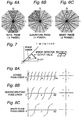
- the modulated signal changes between three kinds of the octal phase, the quadrature phase and the binary phase. Therefore, the signal area in the complex plane is divided into eight areas in the case of the octal phase as shown in Fig. 6A, four areas in the case of the quadrature phase as shown in Fig. 6B, and two in the case of the binary phase as shown in Fig. 6B.
- the received phase of the modulated signal is mapped to the complex plane divided as mentioned above, however, at this time, the error calculating circuit 22 does not recognize the signal area to which the received phase is mapped.
- the error calculating circuit 22 individually calculates the phase error between the received phase of the modulated signal mapped as mentioned above and the reference phase of a plurality of signal areas corresponding to the maximum modulation phase number, as a distance between the mapped position of the modulated signal and the reference straight line, from at least one of the inphase signal I and the quadrature signal Q.
- the maximum modulation phase number is eight phases
- eight distance between the mapped position of the modulated signal and eight reference straight lines are calculated as "Q ⁇ 2", “-I+Q”, “-I ⁇ 2", “-I-Q”, “-Q ⁇ 2”, “I-Q”, “I ⁇ 2” and “I+Q”.
- the error calculating circuit 22 calculates only one of each pair of phase errors which has the same value but different only in positive/negative sign. Therefore, the error calculating circuit 22 actually calculates only "I ⁇ 2", “Q ⁇ 2", "I+Q” and "I-Q”.
- the area discriminating circuit 23 is constituted of for example a combinational circuit formed of a plurality of logic gates, in order to discriminate and determine, on the basis of the inphase signal I and the quadrature signal Q, one to which the received phase is mapped, from a plurality of signal areas corresponding to the modulation phase number of the modulated signal. Namely, as shown in Fig. 4, the area discriminating circuit 23 receives the signal of the inphase signal I, the sign of the quadrature signal Q, the sign of "I+Q", the sign of "I-Q", and the modulation phase number, and outputs five selection signals to the error selecting circuit 24 as the result of the signal area discrimination.
- the area discriminating circuit 23 detects one of the "positive/negative sign of the inphase signal I", the "positive/negative sign of the quadrature signal Q", the "positive/negative sign of the sum of the inphase signal I and the quadrature signal Q", and the "positive/negative sign of the result obtained by subtracting one of the inphase signal I and the quadrature signal Q from the other", for the four area patterns, and selects one from the two signal areas.
- the area discriminating circuit 23 detects one of the "positive and negative combination of the inphase signal I and the quadrature signal Q", and the "positive/negative sign of the result obtained by subtracting one of the inphase signal I and the quadrature signal Q from the other", for the two area patterns, and selects one from the four signal areas.
- the area patterns for the two phases become four, as shown in Figs. 12A, 12B, 12C and 12D.
- Fig. 12A when the reference phase is positioned on the axis of the inphase signal I to become "0°” and "180°", the complex plane is divided into signal areas of "90° to 270°” and "270° to 90°".
- one signal area can be determined from the two signal areas on the basis of the "positive/negative sign of the inphase signal I".
- one signal area can be determined from the two signal areas on the basis of the "positive/negative sign of the result obtained by subtracting one of the inphase signal I and the quadrature signal Q from the other".
- the area patterns for the four phases become two, as shown in Figs. 11A and 11B.
- Fig. 11A when the complex plane is divided into signal areas of "0° to 90°”, “90° to 180°”, “180° to 270°” and “270° to 0°", one signal area can be determined from the four signal areas on the basis of the "positive and negative combination of the inphase signal I and the quadrature signal Q".
- one signal area can be determined from the four signal areas on the basis of the "positive/negative sign of the result obtained by subtracting one of the inphase signal I and the quadrature signal Q from the other".
- the error selecting circuit 24 receives the eight phase errors calculated by the error calculating circuit 22 as mentioned above, and selects one of the eight phase errors, corresponding to the signal area discriminated and determined by the area discriminating circuit 23 as mentioned above. In detail, since the error calculating circuit 22 actually calculates only four of the eight phase errors as mentioned hereinbefore, as shown in Fig. 5, the four phase errors are supplied to each of two signal processing systems of the error selecting circuit 24.
- the error selecting circuit 24 includes a first selecting circuit 41 and a second selecting circuit 42, which include selectors 43 and 44, respectively, for receiving the four phase errors and selecting one of the four phase errors in accordance with the selection signal supplied from the area discriminating circuit 23.
- An output of the selector 43 is connected directly to one input of a selector 47, and through a sign inverting circuit 45 to the other input of the selector 47.
- An output of the selector 47 is connected to one input of a selector 49.
- An output of the selector 44 is connected directly to one input of a selector 48, and through a sign inverting circuit 46 to the other input of the selector 48.
- An output of the selector 48 is connected to the other input of the selector 49.
- An output of the selector 49 is connected to an output terminal for the phase error.
- the error selecting circuit 24 also includes a selection control circuit 51, which includes a selector 51 having a pair of inputs connected to the input and the output of the sign inverting circuit 46. An output of the selector 51 is connected through an inverter 53 to one input of a adder 54, which has the other input connected the output of the selector 47.
- An output of the adder 54 is connected through an inverter 55 to one input of an AND gate 56, which has the other input connected to the selection signal from the area discriminating circuit 23.
- An output of the AND gate 56 is connected to a selection control input of the selector 49.
- the four phase errors are supplied to the two signal processing systems, in which each of the four phase errors is multiplied with "-1" by the sign inverting circuit 45, 46, so that the eight phase errors are generated in total.
- this portion can be considered to be a portion of the error calculating circuit 22.
- phase error is selected in accordance with the signal area discriminated and determined by the area discriminating circuit 23. At this time, even if the modulation phase number of the modulated signal is two phases or four phases, since one signal area is designated by the area discriminating circuit 23, one phase error is correspondingly selected from the eight phase error.
- the two signal processing systems of the error selection circuit 24 select one from the signal areas in the two respective area patterns, so that the, two signal areas are selected in total, and then, the phase errors in the two area patterns are compared to each other, so that a smaller one is selected. Namely, for one received phase, a minimum phase error is calculated in each of the two area patterns for the four phases, and a smaller one is selected from the two minimum phase errors.
- the error detecting circuit 21 in this embodiment can detect the phase error of the PSK modulated signal having the modulation phase number changing in the time division manner, and therefore, the signal demodulating device in this embodiment can demodulate the PSK modulated signal having the modulation phase number changing in the time division manner.
- the PSK modulated signal having the modulation phase number changing between two phases, four phases and eight phases in the time division manner as shown in Fig. 10 is received by the radio receiver antenna 2 of the signal demodulator of the present invention, the inphase signal I and the quadrature signal Q are generated from the received modulated signal by the signal generating circuit 3, and the modulation phase number of the modulated signal changing in the time division manner is detected by the phase number detecting circuit 18.
- the error detecting circuit 21 detects the phase error of the modulated signal, so that the PLL circuit 17, which includes the error detecting circuit 21 as a portion, synchronously demodulates the inphase signal I and the quadrature signal Q generated by the signal generating circuit 3
- the error detecting circuit 21 of this embodiment maps the received phase of the modulated signal to the complex plane divided into a plurality of signal areas in accordance with the modulation phase number of the modulated signal, while allocating the inphase signal I and the quadrature signal Q as values of the axis of abscissas and the axis of ordinates.
- the phase error between the one received phase of the modulated signal mapped as mentioned above and the eight reference phases for eight phases is calculated as the distance between one mapped position of the modulated signal and the eight reference straight line.
- the error calculating circuit 22 calculates only one of each pair of phase errors which has the same value but different only in positive/negative sign, the error calculating circuit 22 actually calculates only "I ⁇ 2", “Q ⁇ 2", "I+Q" and "I-Q".
- phase errors thus calculated are divided into the two signal processing systems, and the signal in only one of the two signal processing systems is multiplied with "-1" by the sign inverting circuit 45, 46. Therefore, the eight phase errors of "Q ⁇ 2", “-I+Q”, "-I ⁇ 2”, “-I-Q”, “-Q ⁇ 2”, “I-Q”, "I ⁇ 2” and “I+Q” are calculated by the error calculating circuit 22.
- the area discriminating circuit 23 discriminates and determines one signal area to which the received phase is mapped, from the plurality of signal areas. Specifically, in the case that the phase number of the modulated signal is the two phases, the area discriminating circuit 23 detects one of the "positive/negative sign of the inphase signal I", the "positive/negative sign of the quadrature signal Q", the "positive/negative sign of the sum of the inphase signal I and the quadrature signal Q", and the "positive/negative sign of the result obtained by subtracting one of the inphase signal I and the quadrature signal Q from the other", for the four area patterns, and selects one from the two signal areas.
- the area discriminating circuit 23 detects one of the "positive and negative combination of the inphase signal I and the quadrature signal Q", and the "positive/negative sign of the result obtained by subtracting one of the inphase signal I and the quadrature signal Q from the other", for the two area patterns, and selects one from the four signal areas.
- the error selecting circuit 24 selects from the eight phase errors one phase error corresponding to the one signal area notified by the area discriminating circuit 23, so that the phase error of the modulated signal is outputted.
- the error selecting circuit 24 selects one phase error. However, when the modulation phase number is eight phases, the error selecting circuit 24 selects a minimum one of the two phase errors which are respectively calculated in the two area patterns for the four phases.
- the error detecting circuit in this embodiment can detect the phase error of the modulated signal having the modulation phase number changing in the time division manner. At this time, the eight phase errors are ceaselessly calculated regardless of the modulation phase number of the modulated signal, and one corresponding to the modulation phase number is selected from the eight phase errors.
- the signal demodulator 1 of this embodiment can appropriately demodulate the modulated signal having the modulation phase number changing in the time division manner.
- the error detecting circuit 21 in this embodiment approximately calculates the phase error of the modulated signal as the distance between the mapped position and the reference straight line, as shown in Fig. 7, the processing for the calculation of the phase error is easy.
- the calculation of the phase error is conducted by the hardware of the error calculating circuit 22, it is possible to speedily calculate a plurality of phase errors.
- the error detecting circuit 21 of this embodiment executes the simple calculation for obtaining the eight phase errors, by means of the hardware having a simple construction, a large scale circuit is no longer required to calculate the phase error of the modulated signal having the changing modulation phase number. Namely, a circuit for calculating the phase error of the modulated signal having the changing modulation phase number can be realized with a small scale circuit.
- one phase error corresponding to the signal area is selected from the eight phase errors calculated as mentioned above. But, since the signal area to which the received phase is mapped is discriminated and determined by the area discriminating circuit 23 on the basis of the inphase signal I, the quadrature signal Q and the modulation phase, when the modulation phase number of the modulated signal is that of the two phases or the four phases, even if the signal area pattern changes, it is possible to select one appropriate phase error from the eight phase errors.
- the various means in the error detecting circuit 21 in the above mentioned embodiment are constituted of respective dedicated hardware.
- various means included in the signal demodulator 1 can be realized by a computer operating with an appropriate software, or alternatively, it is possible that a portion of the various means included in the signal demodulator 1 is realized by software and the other is realized by hardware.
- the various means in the error detecting circuit 21 are realized by software, it is sufficient if the information storing medium such as a RAM or a ROM of a computer is programmed as a program to be executed by the CPU of the computer, to the effect that (1) the received phase of the modulated signal is mapped to the complex plane divided into a plurality of signal areas corresponding to the modulation phase number by allocating the inphase signal and the quadrature signal as values of the axis of abscissas and the axis of ordinates in a complex plane, (2) the phase error between the received phase of the modulated signal thus mapped and the reference phase of each of a plurality of signal areas corresponding to the maximum modulation phase number is individually calculated as the distance between the mapped position of the modulated signal and the reference straight line, from one of the inphase signal and the quadrature signal, (3) one signal area to which the received phase is mapped is discriminated and selected from the plurality of signal areas corresponding to the modulation phase number of the modulated signal, on the
Landscapes
- Engineering & Computer Science (AREA)
- Computer Networks & Wireless Communication (AREA)
- Signal Processing (AREA)
- Digital Transmission Methods That Use Modulated Carrier Waves (AREA)
- Synchronisation In Digital Transmission Systems (AREA)
Applications Claiming Priority (3)
| Application Number | Priority Date | Filing Date | Title |
|---|---|---|---|
| JP328548/97 | 1997-11-28 | ||
| JP32854897 | 1997-11-28 | ||
| JP32854897A JP3185867B2 (ja) | 1997-11-28 | 1997-11-28 | 誤差検出方法および装置、信号復調方法および装置 |
Publications (2)
| Publication Number | Publication Date |
|---|---|
| EP0920162A2 true EP0920162A2 (de) | 1999-06-02 |
| EP0920162A3 EP0920162A3 (de) | 2002-05-02 |
Family
ID=18211517
Family Applications (1)
| Application Number | Title | Priority Date | Filing Date |
|---|---|---|---|
| EP98250418A Withdrawn EP0920162A3 (de) | 1997-11-28 | 1998-11-30 | Verfahren und Anordnung zur Korrektur des Phasenfehlers eines PSK-signals |
Country Status (3)
| Country | Link |
|---|---|
| US (1) | US6334203B1 (de) |
| EP (1) | EP0920162A3 (de) |
| JP (1) | JP3185867B2 (de) |
Families Citing this family (12)
| Publication number | Priority date | Publication date | Assignee | Title |
|---|---|---|---|---|
| US6975691B1 (en) * | 1997-12-17 | 2005-12-13 | Kabushiki Kaisha Kenwood | Receiver |
| JP3206574B2 (ja) * | 1998-12-17 | 2001-09-10 | 日本電気株式会社 | 信号推定装置及びプログラムを記憶した記憶媒体 |
| KR100333704B1 (ko) * | 1999-06-21 | 2002-04-24 | 박종섭 | 위상잡음에 따른 위상회전오류 극복을 위한 결정영역 수정회로 |
| JP3555943B2 (ja) * | 2002-02-27 | 2004-08-18 | 松下電器産業株式会社 | 無線受信装置、変調方式判定方法および符号化方式判定方法 |
| US6735554B2 (en) * | 2002-05-16 | 2004-05-11 | Tektronix, Inc. | Method and apparatus for representing complex vector data |
| EP1463233A3 (de) * | 2002-10-25 | 2004-10-06 | Matsushita Electric Industrial Co., Ltd. | Signalübertragungsverfahren für in Rahmen formatierte Daten unter Verwendung eines Einzelwortes |
| KR100724895B1 (ko) * | 2005-06-17 | 2007-06-04 | 삼성전자주식회사 | 위상고정루프와 위상고정루프에서의 위상 검출방법 및 그를이용하는 수신기 |
| KR100785767B1 (ko) * | 2005-11-11 | 2007-12-18 | 한국전자통신연구원 | 구적오차가 있는 m-psk 시스템의 심볼오율 성능 개선장치 및 방법 |
| US20070160168A1 (en) * | 2006-01-11 | 2007-07-12 | Beukema Troy J | Apparatus and method for signal phase control in an integrated radio circuit |
| EP2415173A1 (de) * | 2009-04-02 | 2012-02-08 | Semiconductor Ideas To The Market (ITOM) | Verfahren zum mischen eines komplexen digitalen signals mit einem referenzsignal, mischer und digital-analog-umsetzer, die das verfahren verwenden |
| US9634878B1 (en) * | 2011-09-08 | 2017-04-25 | See Scan, Inc. | Systems and methods for data transfer using self-synchronizing quadrature amplitude modulation (QAM) |
| US9893916B2 (en) * | 2016-07-01 | 2018-02-13 | Texas Instruments Incorporated | Methods and apparatus for performing a high speed phase demodulation scheme using a low bandwidth phase-lock loop |
Family Cites Families (10)
| Publication number | Priority date | Publication date | Assignee | Title |
|---|---|---|---|---|
| JPS5716546B2 (de) * | 1973-07-12 | 1982-04-06 | ||
| US4866395A (en) * | 1988-11-14 | 1989-09-12 | Gte Government Systems Corporation | Universal carrier recovery and data detection for digital communication systems |
| JPH082060B2 (ja) * | 1989-09-13 | 1996-01-10 | 日本電気株式会社 | 搬送波再生方式およびディジタル位相復調装置 |
| JP2969837B2 (ja) * | 1990-07-10 | 1999-11-02 | ヤマハ株式会社 | π/4シフトQPSK変調信号の判定回路 |
| JPH08186606A (ja) | 1994-12-28 | 1996-07-16 | Toshiba Corp | 受信装置 |
| JP3091120B2 (ja) | 1995-08-16 | 2000-09-25 | 三菱電機株式会社 | Qpsk復調装置 |
| SE506847C2 (sv) * | 1996-06-28 | 1998-02-16 | Ericsson Telefon Ab L M | Förfarande och anordning vid fasmodulerade signaler |
| DE19635813A1 (de) * | 1996-09-04 | 1998-03-05 | Johannes Prof Dr Ing Huber | Verfahren zur Reduktion des Spitzenwertfaktors bei digitalen Übertragungsverfahren |
| JP3115259B2 (ja) | 1997-06-30 | 2000-12-04 | 株式会社ケンウッド | 絶対位相化同期捕捉回路 |
| US5974091A (en) * | 1997-10-30 | 1999-10-26 | Communication Network Systems | Composite trellis system and method |
-
1997
- 1997-11-28 JP JP32854897A patent/JP3185867B2/ja not_active Expired - Fee Related
-
1998
- 1998-11-30 US US09/201,878 patent/US6334203B1/en not_active Expired - Fee Related
- 1998-11-30 EP EP98250418A patent/EP0920162A3/de not_active Withdrawn
Also Published As
| Publication number | Publication date |
|---|---|
| EP0920162A3 (de) | 2002-05-02 |
| US6334203B1 (en) | 2001-12-25 |
| JPH11163956A (ja) | 1999-06-18 |
| JP3185867B2 (ja) | 2001-07-11 |
Similar Documents
| Publication | Publication Date | Title |
|---|---|---|
| US5448602A (en) | Diversity radio receiver | |
| US5729577A (en) | Signal processor with improved efficiency | |
| EP0920162A2 (de) | Verfahren und Anordnung zur Korrektur des Phasenfehlers eines PSK-signals | |
| EP0504890B1 (de) | Demodulator zur Demodulierung eines pi/4-umgetasteten DQPSK-Signals | |
| CA2173530C (en) | Modulation and demodulation method, modulator and demodulator | |
| US5694415A (en) | Signal communication system capable of recognizing reception of reception desired signal | |
| EP1039709B1 (de) | Empfänger für mit einer Vielzahl von PSK-Modulationsschemata modulierte Signale | |
| US5956374A (en) | Jitter suppressing circuit | |
| US6047033A (en) | Apparatus and method for signal timing error detection | |
| US6993096B1 (en) | BS digital broadcasting receiver | |
| JP2001053819A (ja) | 位相回転エラーを補償するための位相検出装置 | |
| CA1269716A (en) | Digital communication system employing carrier phase shift | |
| JP2595961B2 (ja) | デイジタル変復調システム | |
| EP0757462B1 (de) | Korrektur einer Frequenzverschiebung für ein Datenempfangssystem | |
| EP0940005B1 (de) | Verfahren und gerät zur verwendung mit phasenmodulierten signalen | |
| EP0822689B1 (de) | Trägerrückgewinnung in einem PSK-Empfänger | |
| EP0987862B1 (de) | Schaltung zur absoluten Phasensynchronisation | |
| EP1143676B1 (de) | Dekodierungsfehlerfreier diversitätsempfänger, sowie schaltung zur talzurückgewinnung für diversitätsempfänger | |
| EP0996263B1 (de) | Schaltung zur Rechnung der Steuerung einer Signalpunktordnung | |
| KR100317571B1 (ko) | 디지털통신기의심볼간간섭현상억제방법및회로 | |
| JPH10303996A (ja) | 周波数ずれ検出方法と周波数ずれ検出装置 | |
| JPH06296185A (ja) | Psk復調装置及びqpsk復調装置 | |
| JPH06296186A (ja) | Psk復調装置及びqpsk復調装置 | |
| JP2004364131A (ja) | 位相変調信号復調装置及び復調方法 | |
| JPS6219101B2 (de) |
Legal Events
| Date | Code | Title | Description |
|---|---|---|---|
| PUAI | Public reference made under article 153(3) epc to a published international application that has entered the european phase |
Free format text: ORIGINAL CODE: 0009012 |
|
| AK | Designated contracting states |
Kind code of ref document: A2 Designated state(s): AT BE CH CY DE DK ES FI FR GB GR IE IT LI LU MC NL PT SE Kind code of ref document: A2 Designated state(s): DE FR GB |
|
| AX | Request for extension of the european patent |
Free format text: AL;LT;LV;MK;RO;SI |
|
| PUAL | Search report despatched |
Free format text: ORIGINAL CODE: 0009013 |
|
| AK | Designated contracting states |
Kind code of ref document: A3 Designated state(s): AT BE CH CY DE DK ES FI FR GB GR IE IT LI LU MC NL PT SE |
|
| AX | Request for extension of the european patent |
Free format text: AL;LT;LV;MK;RO;SI |
|
| 17P | Request for examination filed |
Effective date: 20020513 |
|
| 17Q | First examination report despatched |
Effective date: 20020730 |
|
| AKX | Designation fees paid |
Free format text: DE FR GB |
|
| RAP1 | Party data changed (applicant data changed or rights of an application transferred) |
Owner name: NEC ELECTRONICS CORPORATION |
|
| GRAP | Despatch of communication of intention to grant a patent |
Free format text: ORIGINAL CODE: EPIDOSNIGR1 |
|
| STAA | Information on the status of an ep patent application or granted ep patent |
Free format text: STATUS: THE APPLICATION IS DEEMED TO BE WITHDRAWN |
|
| 18D | Application deemed to be withdrawn |
Effective date: 20040123 |
|
| RIN1 | Information on inventor provided before grant (corrected) |
Inventor name: INAGAWA, OSAMU |