EP0917260B1 - Electrical isolation of opto-electronic device components - Google Patents
Electrical isolation of opto-electronic device components Download PDFInfo
- Publication number
- EP0917260B1 EP0917260B1 EP97309032A EP97309032A EP0917260B1 EP 0917260 B1 EP0917260 B1 EP 0917260B1 EP 97309032 A EP97309032 A EP 97309032A EP 97309032 A EP97309032 A EP 97309032A EP 0917260 B1 EP0917260 B1 EP 0917260B1
- Authority
- EP
- European Patent Office
- Prior art keywords
- opto
- layer
- contact
- electronic device
- integrated
- Prior art date
- Legal status (The legal status is an assumption and is not a legal conclusion. Google has not performed a legal analysis and makes no representation as to the accuracy of the status listed.)
- Expired - Lifetime
Links
- 238000002955 isolation Methods 0.000 title claims description 50
- 230000005693 optoelectronics Effects 0.000 title claims description 35
- 239000000758 substrate Substances 0.000 claims description 17
- 230000001419 dependent effect Effects 0.000 claims 1
- 239000010410 layer Substances 0.000 description 66
- 238000000034 method Methods 0.000 description 15
- 230000003287 optical effect Effects 0.000 description 10
- 239000004020 conductor Substances 0.000 description 7
- 238000004519 manufacturing process Methods 0.000 description 7
- 238000005530 etching Methods 0.000 description 6
- 238000013459 approach Methods 0.000 description 5
- VYPSYNLAJGMNEJ-UHFFFAOYSA-N Silicium dioxide Chemical compound O=[Si]=O VYPSYNLAJGMNEJ-UHFFFAOYSA-N 0.000 description 4
- 230000002411 adverse Effects 0.000 description 4
- 238000000151 deposition Methods 0.000 description 4
- 238000005334 plasma enhanced chemical vapour deposition Methods 0.000 description 4
- 238000000623 plasma-assisted chemical vapour deposition Methods 0.000 description 4
- 238000010521 absorption reaction Methods 0.000 description 3
- 238000005253 cladding Methods 0.000 description 3
- 238000004891 communication Methods 0.000 description 3
- 238000002513 implantation Methods 0.000 description 3
- 230000010354 integration Effects 0.000 description 3
- 239000013307 optical fiber Substances 0.000 description 3
- 229910001258 titanium gold Inorganic materials 0.000 description 3
- 229910000530 Gallium indium arsenide Inorganic materials 0.000 description 2
- 229910052681 coesite Inorganic materials 0.000 description 2
- 229910052906 cristobalite Inorganic materials 0.000 description 2
- 238000005516 engineering process Methods 0.000 description 2
- 239000010931 gold Substances 0.000 description 2
- 239000000463 material Substances 0.000 description 2
- 239000002184 metal Substances 0.000 description 2
- 229910052751 metal Inorganic materials 0.000 description 2
- 238000012545 processing Methods 0.000 description 2
- 239000000377 silicon dioxide Substances 0.000 description 2
- 229910052682 stishovite Inorganic materials 0.000 description 2
- 229910052905 tridymite Inorganic materials 0.000 description 2
- ZEMPKEQAKRGZGQ-AAKVHIHISA-N 2,3-bis[[(z)-12-hydroxyoctadec-9-enoyl]oxy]propyl (z)-12-hydroxyoctadec-9-enoate Chemical compound CCCCCCC(O)C\C=C/CCCCCCCC(=O)OCC(OC(=O)CCCCCCC\C=C/CC(O)CCCCCC)COC(=O)CCCCCCC\C=C/CC(O)CCCCCC ZEMPKEQAKRGZGQ-AAKVHIHISA-N 0.000 description 1
- 229910001218 Gallium arsenide Inorganic materials 0.000 description 1
- 239000004642 Polyimide Substances 0.000 description 1
- 229910045601 alloy Inorganic materials 0.000 description 1
- 239000000956 alloy Substances 0.000 description 1
- 230000003321 amplification Effects 0.000 description 1
- 230000003667 anti-reflective effect Effects 0.000 description 1
- 230000005540 biological transmission Effects 0.000 description 1
- 230000015572 biosynthetic process Effects 0.000 description 1
- 238000010276 construction Methods 0.000 description 1
- 230000008878 coupling Effects 0.000 description 1
- 238000010168 coupling process Methods 0.000 description 1
- 238000005859 coupling reaction Methods 0.000 description 1
- 238000005520 cutting process Methods 0.000 description 1
- 230000008021 deposition Effects 0.000 description 1
- 238000010586 diagram Methods 0.000 description 1
- 230000000694 effects Effects 0.000 description 1
- 230000005684 electric field Effects 0.000 description 1
- 230000007613 environmental effect Effects 0.000 description 1
- 238000010438 heat treatment Methods 0.000 description 1
- 238000013101 initial test Methods 0.000 description 1
- 238000005468 ion implantation Methods 0.000 description 1
- 238000010884 ion-beam technique Methods 0.000 description 1
- 238000003199 nucleic acid amplification method Methods 0.000 description 1
- 238000013021 overheating Methods 0.000 description 1
- 229920001721 polyimide Polymers 0.000 description 1
- 230000001681 protective effect Effects 0.000 description 1
- 230000005701 quantum confined stark effect Effects 0.000 description 1
- 239000004065 semiconductor Substances 0.000 description 1
- 238000000926 separation method Methods 0.000 description 1
- 235000012239 silicon dioxide Nutrition 0.000 description 1
- 239000002356 single layer Substances 0.000 description 1
- 238000012360 testing method Methods 0.000 description 1
Images

Classifications
-
- H—ELECTRICITY
- H01—ELECTRIC ELEMENTS
- H01S—DEVICES USING THE PROCESS OF LIGHT AMPLIFICATION BY STIMULATED EMISSION OF RADIATION [LASER] TO AMPLIFY OR GENERATE LIGHT; DEVICES USING STIMULATED EMISSION OF ELECTROMAGNETIC RADIATION IN WAVE RANGES OTHER THAN OPTICAL
- H01S5/00—Semiconductor lasers
- H01S5/02—Structural details or components not essential to laser action
- H01S5/026—Monolithically integrated components, e.g. waveguides, monitoring photo-detectors, drivers
- H01S5/0265—Intensity modulators
-
- H—ELECTRICITY
- H01—ELECTRIC ELEMENTS
- H01S—DEVICES USING THE PROCESS OF LIGHT AMPLIFICATION BY STIMULATED EMISSION OF RADIATION [LASER] TO AMPLIFY OR GENERATE LIGHT; DEVICES USING STIMULATED EMISSION OF ELECTROMAGNETIC RADIATION IN WAVE RANGES OTHER THAN OPTICAL
- H01S5/00—Semiconductor lasers
- H01S5/04—Processes or apparatus for excitation, e.g. pumping, e.g. by electron beams
- H01S5/042—Electrical excitation ; Circuits therefor
- H01S5/0425—Electrodes, e.g. characterised by the structure
- H01S5/04256—Electrodes, e.g. characterised by the structure characterised by the configuration
-
- H—ELECTRICITY
- H01—ELECTRIC ELEMENTS
- H01S—DEVICES USING THE PROCESS OF LIGHT AMPLIFICATION BY STIMULATED EMISSION OF RADIATION [LASER] TO AMPLIFY OR GENERATE LIGHT; DEVICES USING STIMULATED EMISSION OF ELECTROMAGNETIC RADIATION IN WAVE RANGES OTHER THAN OPTICAL
- H01S5/00—Semiconductor lasers
- H01S5/20—Structure or shape of the semiconductor body to guide the optical wave ; Confining structures perpendicular to the optical axis, e.g. index or gain guiding, stripe geometry, broad area lasers, gain tailoring, transverse or lateral reflectors, special cladding structures, MQW barrier reflection layers
- H01S5/22—Structure or shape of the semiconductor body to guide the optical wave ; Confining structures perpendicular to the optical axis, e.g. index or gain guiding, stripe geometry, broad area lasers, gain tailoring, transverse or lateral reflectors, special cladding structures, MQW barrier reflection layers having a ridge or stripe structure
Definitions
- the present invention relates generally to the electrical isolation of components within an integrated opto-electronic device where two or more active regions are optically coupled, for example by a waveguide.
- the invention particularly relates to isolation of a distributed feed-back (DFB) laser diode and an electro-absorption (EA) modulator in a monolithically integrated opto-electronic transmitter device for a fibre-optic telecommunications link.
- DFB distributed feed-back
- EA electro-absorption
- Opto-electronic integration gives the potential for low cost, reliable and compact components, improved temperature and mechanical stability, and assured alignment between components.
- the integration of a laser diode with a modulator for example in a buried heterostructure or a ridge stripe, was achieved many years ago, for example see the publication by S. Tarucha and H. Okamoto in Appl. Phys. Lett., vol. 22, pp. 242-243, 1986, relating to a device fabricated from GaAs.
- such integrated opto-electronic transmitter devices are usually fabricated from on a wafer grown from an n ++ -InP substrate on which are grown a number of layers, including a p + -InP active layer capped by a p ++ -GaInAs ternary or cap layer.
- the cap layer has a relatively low resistance, and so serves as a contact layer to which electrical contacts may be made.
- the light output from the laser diode should have a steady wavelength and intensity.
- the electrical resistance between the laser diode and modulator (referred to herein as the isolation resistance) will be about 1-10 k ⁇ , depending on the conductivity of the p-contact material and the separation of the contacts. It is therefore possible that the electrical signal used to modulate the modulator can inadvertently affect the laser diode, causing wavelength and/or intensity shifts.
- the isolation resistance therefore needs to be increased, at least to a few 100 k ⁇ , and preferably to a few M ⁇ .
- One approach is to etch through the ternary cap layer. This increases the isolation resistance only to about 10-20 k ⁇ . Although such etching does not interfere with the optical waveguide between the laser diode and the modulator, this is insufficient isolation.
- the second embodiment in this document is an integrated optoelectronic device with two components: a light-emitting element, i.e. a laser diode, and a light modulator.
- a grounded third electrode is provided in the isolation region, on a semiconductor contact layer. This grounded electrode provides electrostatical shielding, avoiding the high frequency signal induced from the electrode of the light modulator to be transmitted to the electrode of the light-emitting element. Consequently, this light-emitting element can operate stably.
- an integrated opto-electronic device comprising at least two opto-electronic components fabricated on the same substrate, two of the components being: separated by an electrical isolation region; linked optically across the isolation region by a waveguide; and capped by a contact layer through which ohmic contacts are made to operate the components, characterised in that the contact layer extends through the isolation region from which a grounding contact is made to ground the contact layer in the isolation region and so electrically isolate the two components from each other.
- the grounding contact may then draw any stray currents from one of said two components which could adversely affect the performance of the other of said component.
- the component being a laser diode
- the other component being a modulator, for example an EA modulator, for modulating the output of the laser diode
- stray modulation currents at the modulation frequency may be drawn to the grounding contact in order to prevent wavelength or intensity chirping of the otherwise steadily biased laser diode.
- a passivating layer covers the cap layer in order to provide environmental protection for the device.
- the passivating layer may then have contact windows in the passivating layer through which the contacts are made.
- the integrated device will have a ground plane, for example either the substrate or a layer grown on the substrate.
- the device will be fabricated so that the substrate is a ground plane.
- the grounding contact from the cap layer may then be made to the ground plane. If a contact window is provided to the substrate, then the grounding contact may conveniently be made through this window to the ground plane. It would however, be possible for the grounding contact to be made, for example by a wire, or some other suitable grounding point.
- the ground plane need not necessarily be a zero volts with respect to the earth, but will be at a suitable potential with respect to the components in order to draw stray currents away from one or more of the components. However, it may be the case that at least one of the components is grounded by the ground plane.
- a passivating layer extends over the device, and in a preferred embodiment of the invention, this device passivating layer is contiguous with the cap passivating layer.
- the window to the substrate may then extend through the device passivating layer in order to provide a convenient route to the ground plane.
- the contacts may be convenient to fabricate one or each of the contacts by depositing a conducting layer, rather than by using wires.
- This deposited conducting layer may then cover over one or more windows.
- the contacts are deposited so that the contacts cover over fully all of the contact windows.
- the deposited conducting layer(s) may then act as a type of passivating layer in the area of the windows not otherwise protected by the aforementioned passivating layer.
- a resistance may be provided in line with the current path to ground. At least part of this resistance may conveniently be provided by the cap layer, which may be fabricated with dimensions depending on the material of the cap layer to give at least 1 k ⁇ between a component and the ground contact.
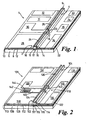
- Figure 1 shows, not to scale, an integrated prior art opto-electronic device 1 comprising two components, namely a DFB laser diode 2 and an EA modulator 4, suitable for use as a transmitter in a high speed fibre-optic link operating at 1.55 ⁇ m.
- a DFB laser diode 2 and an EA modulator 4
- high speed links operate at 2.5 or 10 Gbits/s, and bit rates of up to 40 Gbits/s have been demonstrated in the laboratory.
- the device 1 is grown in wafer form, from an n ++ -InP substrate 6 doped to around 10 19 cm -3 , on which is grown a 2 ⁇ m thick n + -InP buffer layer 8 doped to around 10 18 cm -3 .
- the laser diode has an In x Ga 1-x As 1-y P y active layer 10 which is about 100 nm to 300 nm thick, and this is topped by another buffer layer 12, here a "cladding" layer formed from p + -InP.
- the DFB grating for the laser diode can be contained in the n + -InP buffer layer or in the p + -InP cap layer.
- the active region of the DFB laser and the EA modulator usually comprises a multiple quantum well (MQW) structure.
- MQW structure is especially advantageous in the modulator section where the absorption edge of the modulator can be shifted towards longer wavelengths by the application of an electric field (the quantum confined Stark effect).
- the output facet 9 of the modulator is anti-reflective coated for good transmission through the facet, and the back facet 11 of the laser diode may be reflectively coated or left uncoated.
- the cladding or upper buffer layer 12 is grown to be about 2 ⁇ m thick, on top of which a 100 nm to 200 nm thick cap layer is deposited.
- the cap layer is formed from p ++ -GaInAs, highly doped to around 10 19 cm -3 , in order to provide a good low resistance ohmic contact for the electrical connection to the laser diode 2.
- the wafer is coated with an oxide layer, here SiO2 (not illustrated deposited by in a plasma enhanced chemical vapour deposition (PECVD) process.
- PECVD plasma enhanced chemical vapour deposition
- This oxide layer is photolithographicly patterned and dry etched to remove the cap layer 16 and all but 200 nm of buffer layer except along a 3 ⁇ m wide ridge stripe 14. The ridge strip 14 therefore rises about 2 ⁇ m above the surrounding surface.
- PECVD oxide layer is removed from the ridge strip to expose again the cap layer 16.
- the ridge stripe 14 has the effect of guiding an optical mode 15 along an active region 17 beneath the stripe 14.
- the ridge stripe 14 extends from the laser diode 2 towards the EA modulator 4 through an isolation region 18.
- the EA modulator has a similar structure to that described for the laser diode, except that the absorption edge of the unbiased modulator is at a shorter wavelength (typically 30 nm to 100 nm shorter) than the gain maximum and the emission wavelength of the laser diode.
- the isolation region 18 comprises a gap 20 etched in a process similar to that described above to remove completely the cap layer 16, and if needed the top of the upper p + -InP buffer layer 12.
- the etching of the gap 20 stops short of the depth which would cause reflections and interfere with light guided by the active region 17 extending underneath the stripe 14. Because of the need to maximise the isolation resistance without adversely affecting the optical properties of the ridge waveguide, and also the need to align the photolithographic pattern with the ridge 14 between the components 2,4, the positioning and etching of the gap is a highly critical process. It is very difficult to achieve this alignment in a production environment.
- the isolation region 18 so produced approximately doubles the isolation resistance between the laser diode 2 and modulator 4. Proton implantation could be used to increase this isolation resistance further to 1-10 M ⁇ .
- the cap layer 16, the sides of the ridge stripe 14, and the surrounding upper buffer layer 10 are then coated with a PECVD oxide layer 22, here an SiO 2 layer. This is pattered and etched in a similar process to that described above, to open up two contact windows on the ridge stripe 14, one 24 above the laser diode and the other 26 above the modulator.
- Metal is then vacuum deposited on the device 1 using well known techniques in two stages, first with a TiPt layer which is patterned using a lift-off process, and then final depositing of a TiAu layer, followed by metal wet etch in a photolithographically defined areas.
- the remaining TiAu layer forms two contacts 28,30 which cover over the contact windows 24,26 to make good ohmic contacts through the cap layer with the laser diode 2 and modulator 4.
- Six other metalised areas 31-36 are also formed that do not make any electrical connection but onto which pads (not shown) may be plated in order to provide physical protection to the ridge stripe 14.
- the substrate 6 would be soldered onto a heat sink in a conventional manner.
- the prior art device 1 is about 700 ⁇ m long (ie in the direction of the ridge 14) and about 300 ⁇ m wide.
- the lengths of the laser diode 2, gap isolation region 18 and modulator 4 are, respectively about 450 ⁇ m, 50 ⁇ m and 200 ⁇ m.
- FIGS 2 and 3 illustrate, not to scale, an integrated opto-electronic device 101 according to the invention.
- This device 101 is similar to the prior art device 1 described above, and so similar features are indicated with reference numerals incremented by 100.
- the device 101 has an isolation region 118 that is about 70 ⁇ m in length, and so is slightly longer than the prior art 18 isolation region. This allows sufficient space for an isolation contact window 140 formed to an unbroken cap layer 116 extending between the laser diode 102 and the modulator 104.
- the isolation contact window 140 is formed in the same manner and at the same time as the contact windows 124,126 for the components 102,104. This is much more convenient than the formation of the isolation gap described above, avoiding the need to align the isolation region in a separate process step from the alignment of the contact windows.
- a ground contact window 142 to the substrate is formed into the device, passing through the buffer layers 108,112, active layer 110 and about 2 ⁇ m into the 100 ⁇ m thick substrate 106.
- the substrate is an effective ground plane for the components 102,104.
- the sides 144 and base (not shown) of the of the ground window 142 are also covered in the oxide layer.
- the oxide covering the base of the ground window 142 is then removed in the same process step which opens up the contact 124,126 and isolation 140 windows.
- a TiPt/TiAu conductor 146 is deposited between the isolation contact window 140 and the ground contact window 142, at the same time as the component conductors 128,130 are deposited.
- a 10 ⁇ m gap separates the conductors 128,130 from the ground conductor 146.
- This method is quite convenient as there are no additional process steps. It has been observed, however, that for devices created under particular processing conditions, the junction between the TiPt and the n++ substrate, that the junction behaves like a Schottky diode. It is therefore preferred if the portion of the conductor 146 away from the ridge stripe is formed in a separate process step from a single layer of AuGeNi or AuSn alloy.
- the integrated construction described above is believed to be particularly advantageous because it facilitates conduction of very high frequency (of the order 1-10 GHz, or even higher) stray currents induced by the modulation.
- the device described above is of relatively low integration density. Because of the ample space afforded by the area to the left side (as drawn) of the ridge, the ground window 142 can be relatively large compared with the contact 124,126 and-isolation 140 windows. In this example, the ground window is 50 ⁇ m wide (in the direction of the ridge 14) and 100 ⁇ m long. The alignment of the ground window with respect to the other features is therefore not as critical as the alignment of the cap layer gap 20 of the prior art device. Furthermore, the depth of the ground window is not critical in order to achieve a good path to ground in the substrate 106. This embodiment of the device is therefore very well suited to a production environment.
- an Au contact pad 158 is plated to metalised area 128, and Au protective pads 162,163,165,166 are plated to metalised areas 132,133,135,136.
- Contact pad 158 is provided only to facilitate initial testing of the laser diode. After testing, the device may then be packaged in an industry standard package (not shown), with a single mode optical fibre coupled with a spherical lens to the output facet of the modulator 104, and with gold bond wires soldered onto metalised areas 128 and 130
- Figure 4 shows electrically how the isolation region 118 helps to isolate the steady laser diode 102 from electrical disturbance from the modulator 104.
- the laser diode is forward biased by a V LD at about 1.6 V, and the modulator is reverse biased with a modulation V M , modulated between -0.5 V (transmissive) and -2.0 V (absorptive) at up to 10 Gbit/s, or higher.
- V M modulation
- a stray current from the laser diode 102 to the modulator 104 varying between about 0.5 mA and 0.9 mA, would cause wavelength or intensity chirping of the laser.
- the unbroken cap layer 116 between the laser diode 102 and modulator 104 provides a relatively low resistance path R i path to the isolation window, and to the substrate ground 106 through the conductor 146. Any stray currents in the cladding or upper buffer layer 112, which has a resistivity of 5 ⁇ 10 -4 ⁇ .m (about ten times higher than that for the cap layer) will also be drawn toward the cap layer 116 between the components 102,104, and from there to ground 106.
- the value of R 1 is preferred to be about 2-3 k ⁇ . A value for R i below about 1 k ⁇ could cause excessive heating of the laser diode, leading to a wavelength shift of the laser diode.
- an optical waveguide with a split into two waveguides at a Y-junction may have electrically driven or modulated active optical regions in two or three of the arms of the "Y", for example an optical amplifier or modulator. It may then be desirable to provide an isolation region at the junction of the three arms with which to electrically isolate the two or three optically active regions.
- tunable DFB laser diodes may be formed from two or three in-line sections, with a tunable Bragg grating section adjacent to a steady state amplification section.
- Opto-electronic devices according to the invention provide a convenient and economical means of electrically isolating integrated opto-electronic components.
- the process steps involved may be similar to other standard steps used in the fabrication of such devices. There is no need for additional expensive processing equipment not used in other steps, such as ion beam implantation equipment.
- the tolerances in the alignment of the isolation region, and grounding contacts or windows may be reduced compared with those of prior art isolation regions.
Landscapes
- Physics & Mathematics (AREA)
- Condensed Matter Physics & Semiconductors (AREA)
- General Physics & Mathematics (AREA)
- Electromagnetism (AREA)
- Optics & Photonics (AREA)
- Semiconductor Lasers (AREA)
- Optical Modulation, Optical Deflection, Nonlinear Optics, Optical Demodulation, Optical Logic Elements (AREA)
- Optical Integrated Circuits (AREA)
- Optical Couplings Of Light Guides (AREA)
Priority Applications (5)
| Application Number | Priority Date | Filing Date | Title |
|---|---|---|---|
| EP97309032A EP0917260B1 (en) | 1997-11-11 | 1997-11-11 | Electrical isolation of opto-electronic device components |
| DE69721272T DE69721272T2 (de) | 1997-11-11 | 1997-11-11 | Elektrische Isolierung optoelektronischer Bauelemente |
| US09/152,577 US6191464B1 (en) | 1997-11-11 | 1998-09-14 | Electrical isolation of opto-electronic device components |
| CA002247560A CA2247560A1 (en) | 1997-11-11 | 1998-09-16 | Electrical isolation of opto-electronic device components |
| JP31884298A JP4763867B2 (ja) | 1997-11-11 | 1998-11-10 | 光電子装置コンポーネントの電気的分離 |
Applications Claiming Priority (1)
| Application Number | Priority Date | Filing Date | Title |
|---|---|---|---|
| EP97309032A EP0917260B1 (en) | 1997-11-11 | 1997-11-11 | Electrical isolation of opto-electronic device components |
Publications (2)
| Publication Number | Publication Date |
|---|---|
| EP0917260A1 EP0917260A1 (en) | 1999-05-19 |
| EP0917260B1 true EP0917260B1 (en) | 2003-04-23 |
Family
ID=8229607
Family Applications (1)
| Application Number | Title | Priority Date | Filing Date |
|---|---|---|---|
| EP97309032A Expired - Lifetime EP0917260B1 (en) | 1997-11-11 | 1997-11-11 | Electrical isolation of opto-electronic device components |
Country Status (5)
| Country | Link |
|---|---|
| US (1) | US6191464B1 (cg-RX-API-DMAC7.html) |
| EP (1) | EP0917260B1 (cg-RX-API-DMAC7.html) |
| JP (1) | JP4763867B2 (cg-RX-API-DMAC7.html) |
| CA (1) | CA2247560A1 (cg-RX-API-DMAC7.html) |
| DE (1) | DE69721272T2 (cg-RX-API-DMAC7.html) |
Families Citing this family (18)
| Publication number | Priority date | Publication date | Assignee | Title |
|---|---|---|---|---|
| SE520139C2 (sv) | 2001-11-30 | 2003-06-03 | Optillion Ab | Lasermodulator med elektriskt separerade laser- och modulatorsektioner |
| AU2003251607A1 (en) * | 2003-06-24 | 2005-02-14 | Emcore Corporation | Mechanical protection for semiconductor edge-emitting ridge waveguide lasers |
| JP5086141B2 (ja) * | 2008-03-17 | 2012-11-28 | 日本オクラロ株式会社 | 電界吸収型変調器 |
| US9054813B2 (en) * | 2013-03-13 | 2015-06-09 | Source Photonics (Chengdu) Co. Ltd. | Optical transceiver with isolated modulator contacts and/or inputs |
| US9306372B2 (en) | 2013-03-14 | 2016-04-05 | Emcore Corporation | Method of fabricating and operating an optical modulator |
| US9059801B1 (en) | 2013-03-14 | 2015-06-16 | Emcore Corporation | Optical modulator |
| US9306672B2 (en) * | 2013-03-14 | 2016-04-05 | Encore Corporation | Method of fabricating and operating an optical modulator |
| JP2015109319A (ja) * | 2013-12-03 | 2015-06-11 | 日本電信電話株式会社 | 狭線幅レーザ |
| EP3192136B1 (en) * | 2014-09-08 | 2020-10-07 | Lumentum Technology UK Limited | Monolithically integrated tunable semiconductor laser |
| US9564733B2 (en) | 2014-09-15 | 2017-02-07 | Emcore Corporation | Method of fabricating and operating an optical modulator |
| JP6421708B2 (ja) * | 2015-06-29 | 2018-11-14 | 住友電気工業株式会社 | 半導体光素子を作製する方法及び半導体光素子 |
| CN107306009B (zh) * | 2016-04-25 | 2021-04-13 | 住友电工光电子器件创新株式会社 | 在承载体上提供共面线的光发射器 |
| US10074959B2 (en) | 2016-08-03 | 2018-09-11 | Emcore Corporation | Modulated laser source and methods of its fabrication and operation |
| WO2018091094A1 (en) | 2016-11-17 | 2018-05-24 | Fraunhofer-Gesellschaft zur Förderung der angewandten Forschung e.V. | Method for fabricating an electro-absorption modulated laser and electro-absorption modulated laser |
| CN115428280B (zh) * | 2020-04-27 | 2025-04-04 | 三菱电机株式会社 | 半导体光集成元件 |
| US11681166B2 (en) * | 2020-10-28 | 2023-06-20 | II-VI Delware, Inc. | Electro-absorption optical modulator including ground shield |
| CN113540969B (zh) * | 2021-07-16 | 2022-04-22 | 杰创半导体(苏州)有限公司 | 自带偏置电压电路的电调制激光器及其制作方法 |
| CN117394138B (zh) * | 2023-10-07 | 2024-10-29 | 武汉云岭光电股份有限公司 | 电吸收调制器激光器及其制备方法 |
Family Cites Families (5)
| Publication number | Priority date | Publication date | Assignee | Title |
|---|---|---|---|---|
| US5067809A (en) * | 1989-06-09 | 1991-11-26 | Oki Electric Industry Co., Ltd. | Opto-semiconductor device and method of fabrication of the same |
| JP2606078B2 (ja) * | 1993-06-25 | 1997-04-30 | 日本電気株式会社 | 半導体レーザアレイおよびその製造方法 |
| JP3254053B2 (ja) * | 1993-08-09 | 2002-02-04 | 株式会社日立製作所 | 光集積回路 |
| JPH07221400A (ja) * | 1994-01-31 | 1995-08-18 | Fujitsu Ltd | 光変調器集積化発光装置及びその製造方法 |
| JP2842292B2 (ja) * | 1994-09-16 | 1998-12-24 | 日本電気株式会社 | 半導体光集積装置および製造方法 |
-
1997
- 1997-11-11 EP EP97309032A patent/EP0917260B1/en not_active Expired - Lifetime
- 1997-11-11 DE DE69721272T patent/DE69721272T2/de not_active Expired - Lifetime
-
1998
- 1998-09-14 US US09/152,577 patent/US6191464B1/en not_active Expired - Lifetime
- 1998-09-16 CA CA002247560A patent/CA2247560A1/en not_active Abandoned
- 1998-11-10 JP JP31884298A patent/JP4763867B2/ja not_active Expired - Fee Related
Also Published As
| Publication number | Publication date |
|---|---|
| DE69721272T2 (de) | 2004-02-05 |
| EP0917260A1 (en) | 1999-05-19 |
| JP4763867B2 (ja) | 2011-08-31 |
| DE69721272D1 (de) | 2003-05-28 |
| JPH11224970A (ja) | 1999-08-17 |
| US6191464B1 (en) | 2001-02-20 |
| CA2247560A1 (en) | 1999-05-11 |
Similar Documents
| Publication | Publication Date | Title |
|---|---|---|
| EP0917260B1 (en) | Electrical isolation of opto-electronic device components | |
| US6455338B1 (en) | Method of manufacturing an integrated semiconductor laser-modulator device | |
| US20240170914A1 (en) | Semiconductor sub-assemblies for emitting modulated light | |
| US6995454B2 (en) | Semiconductor optical integrated device having a light emitting portion, a modulation section and a separation portion | |
| JP2008010484A (ja) | 半導体光素子及び光送信モジュール | |
| GB2200797A (en) | Semiconductor integrated light emitting device | |
| US5742423A (en) | Semiconductor optical modulator | |
| JPWO1990009047A1 (ja) | 集積化光半導体装置およびその製造方法 | |
| US6931041B2 (en) | Integrated semiconductor laser device and method of manufacture thereof | |
| US5481559A (en) | Light modulator integrated light-emitting device and method of manufacturing the same | |
| US5179567A (en) | Semiconductor laser device, method of fabricating the same and optical system of utilizing the same | |
| JPH0732279B2 (ja) | 半導体発光素子 | |
| US6509580B2 (en) | Semiconductor device with current confinement structure | |
| US20050185689A1 (en) | Optoelectronic device having a Discrete Bragg Reflector and an electro-absorption modulator | |
| US5811838A (en) | Electro-absorption type semiconductor optical modulator | |
| WO2001013479A1 (en) | Modulator and integrated circuit | |
| JP3254053B2 (ja) | 光集積回路 | |
| US6263140B1 (en) | Optoelectronic module | |
| EP1372229B1 (en) | Integrated semiconductor laser and waveguide device | |
| JP4105618B2 (ja) | 半導体光変調導波路 | |
| WO2001067570A2 (en) | Buried mesa semiconductor device | |
| JPH10275960A (ja) | 光半導体素子 | |
| US7606279B1 (en) | Thin INP spacer layer in a high speed laser for reduced lateral current spreading | |
| EP1339108A1 (en) | Semiconductor device with current confinement structure | |
| JP4283079B2 (ja) | 半導体光電子導波路 |
Legal Events
| Date | Code | Title | Description |
|---|---|---|---|
| PUAI | Public reference made under article 153(3) epc to a published international application that has entered the european phase |
Free format text: ORIGINAL CODE: 0009012 |
|
| AK | Designated contracting states |
Kind code of ref document: A1 Designated state(s): DE FR GB SE |
|
| AX | Request for extension of the european patent |
Free format text: AL;LT;LV;MK;RO;SI |
|
| 17P | Request for examination filed |
Effective date: 19990726 |
|
| AKX | Designation fees paid |
Free format text: DE FR GB SE |
|
| RAP1 | Party data changed (applicant data changed or rights of an application transferred) |
Owner name: HEWLETT-PACKARD COMPANY, A DELAWARE CORPORATION |
|
| RAP1 | Party data changed (applicant data changed or rights of an application transferred) |
Owner name: AGILENT TECHNOLOGIES, INC. |
|
| 17Q | First examination report despatched |
Effective date: 20010606 |
|
| RAP1 | Party data changed (applicant data changed or rights of an application transferred) |
Owner name: AGILENT TECHNOLOGIES INC. |
|
| RAP1 | Party data changed (applicant data changed or rights of an application transferred) |
Owner name: AGILENT TECHNOLOGIES INC. A DELAWARE CORPORATION |
|
| RAP1 | Party data changed (applicant data changed or rights of an application transferred) |
Owner name: AGILENT TECHNOLOGIES, INC. (A DELAWARE CORPORATION |
|
| GRAG | Despatch of communication of intention to grant |
Free format text: ORIGINAL CODE: EPIDOS AGRA |
|
| GRAG | Despatch of communication of intention to grant |
Free format text: ORIGINAL CODE: EPIDOS AGRA |
|
| GRAH | Despatch of communication of intention to grant a patent |
Free format text: ORIGINAL CODE: EPIDOS IGRA |
|
| GRAH | Despatch of communication of intention to grant a patent |
Free format text: ORIGINAL CODE: EPIDOS IGRA |
|
| GRAA | (expected) grant |
Free format text: ORIGINAL CODE: 0009210 |
|
| RIC1 | Information provided on ipc code assigned before grant |
Ipc: 7H 01S 5/02 A |
|
| AK | Designated contracting states |
Designated state(s): DE FR GB SE |
|
| PG25 | Lapsed in a contracting state [announced via postgrant information from national office to epo] |
Ref country code: FR Free format text: LAPSE BECAUSE OF FAILURE TO SUBMIT A TRANSLATION OF THE DESCRIPTION OR TO PAY THE FEE WITHIN THE PRESCRIBED TIME-LIMIT Effective date: 20030423 |
|
| REG | Reference to a national code |
Ref country code: GB Ref legal event code: FG4D |
|
| REF | Corresponds to: |
Ref document number: 69721272 Country of ref document: DE Date of ref document: 20030528 Kind code of ref document: P |
|
| PG25 | Lapsed in a contracting state [announced via postgrant information from national office to epo] |
Ref country code: SE Free format text: LAPSE BECAUSE OF FAILURE TO SUBMIT A TRANSLATION OF THE DESCRIPTION OR TO PAY THE FEE WITHIN THE PRESCRIBED TIME-LIMIT Effective date: 20030723 |
|
| PLBE | No opposition filed within time limit |
Free format text: ORIGINAL CODE: 0009261 |
|
| STAA | Information on the status of an ep patent application or granted ep patent |
Free format text: STATUS: NO OPPOSITION FILED WITHIN TIME LIMIT |
|
| 26N | No opposition filed |
Effective date: 20040126 |
|
| EN | Fr: translation not filed | ||
| REG | Reference to a national code |
Ref country code: GB Ref legal event code: 732E |
|
| PGFP | Annual fee paid to national office [announced via postgrant information from national office to epo] |
Ref country code: GB Payment date: 20061122 Year of fee payment: 10 |
|
| GBPC | Gb: european patent ceased through non-payment of renewal fee |
Effective date: 20071111 |
|
| PG25 | Lapsed in a contracting state [announced via postgrant information from national office to epo] |
Ref country code: GB Free format text: LAPSE BECAUSE OF NON-PAYMENT OF DUE FEES Effective date: 20071111 |
|
| PGFP | Annual fee paid to national office [announced via postgrant information from national office to epo] |
Ref country code: DE Payment date: 20161020 Year of fee payment: 20 |
|
| REG | Reference to a national code |
Ref country code: DE Ref legal event code: R071 Ref document number: 69721272 Country of ref document: DE |