EP0904590B1 - VORRICHTUNG ZUR VERARBEITUNG VON ABGETASTETEN ANALOGEN SIGNALEN INDIGITALEN BiCMOS-VERFAHREN - Google Patents
VORRICHTUNG ZUR VERARBEITUNG VON ABGETASTETEN ANALOGEN SIGNALEN INDIGITALEN BiCMOS-VERFAHREN Download PDFInfo
- Publication number
- EP0904590B1 EP0904590B1 EP97928571A EP97928571A EP0904590B1 EP 0904590 B1 EP0904590 B1 EP 0904590B1 EP 97928571 A EP97928571 A EP 97928571A EP 97928571 A EP97928571 A EP 97928571A EP 0904590 B1 EP0904590 B1 EP 0904590B1
- Authority
- EP
- European Patent Office
- Prior art keywords
- transistor
- common
- input
- transistors
- bipolar
- Prior art date
- Legal status (The legal status is an assumption and is not a legal conclusion. Google has not performed a legal analysis and makes no representation as to the accuracy of the status listed.)
- Expired - Lifetime
Links
- 238000000034 method Methods 0.000 title claims description 42
- 230000008569 process Effects 0.000 title claims description 18
- 239000000470 constituent Substances 0.000 claims 1
- 230000008859 change Effects 0.000 description 7
- 239000003990 capacitor Substances 0.000 description 6
- 230000006870 function Effects 0.000 description 4
- 230000003071 parasitic effect Effects 0.000 description 3
- 230000001419 dependent effect Effects 0.000 description 2
- 238000006243 chemical reaction Methods 0.000 description 1
- 239000002131 composite material Substances 0.000 description 1
- 238000012986 modification Methods 0.000 description 1
- 230000004048 modification Effects 0.000 description 1
- 230000004044 response Effects 0.000 description 1
- 238000005070 sampling Methods 0.000 description 1
Images
Classifications
-
- G—PHYSICS
- G11—INFORMATION STORAGE
- G11C—STATIC STORES
- G11C27/00—Electric analogue stores, e.g. for storing instantaneous values
- G11C27/02—Sample-and-hold arrangements
- G11C27/024—Sample-and-hold arrangements using a capacitive memory element
- G11C27/028—Current mode circuits, e.g. switched current memories
Definitions
- the present invention relates to a device for processing sampled analogue signals in a digital BiCMOS process.
- the switched current (SI) technique is a relatively new analog sampled data signal processing technique, that fully exploits digital CMOS technology, see for example "Switched currents, an analogue technique in digital technology" by C. Toumazou, J.B. Hughes and N.C. Battersby, Peter Peregrinius Ltd, 1993.
- the ultimate performance of the SI circuits is primarily determined by the transconductance g m of an MOS transistor and the capacitance Cg seen by its gate. Although a high speed operation (around 100 Mhz) is possible, the performance of speed and accuracy is limited by the technique itself. In order to have high accuracy, large Cg is usually required, since the clock feedthrough error is inversely proportional to Cg.
- a technique for a high speed sampled-data signal processing in BiCMOS see for example "A new BiCMOS technique for very fast discrete time signal processing" by P. Shak and C. Toumazou in Proc. 1995 International Symposium on Circuits and Systems pp. 323-326. It breaks the limitation of g m /Cg of the SI circuits by utilizing bipolar transistors. It first converts a current to a voltage by a transresistor and then converts the voltage to a current by a transconductor. The voltage is sampled and held at the input of the transconductor, whose input device is an MOS transistor. However, the conversion accuracy is determined by the absolute value of the components. For example, the resistor determines the transresistance value, and the transistor size and the operation condition determine the transconductance value. Therefore the technique is sensitive to process variation and another drawback is its complexity.
- CMOS complementary metal-oxide-semiconductor
- advantages over the prior SI technique in CMOS are higher speed, smaller errors, and higher accuracy.
- advantages over other techniques in BiCMOS such as mentioned in the background of the invention are smaller errors and higher accuracy.
- the unique feature of the invented technique is the combination of high input impedance of the MOS devices and high transconductance of the bipolar devices, where both devices are only available in BiCMOS process and not in the CMOS process.
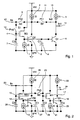
- Figure 1 is a circuit configuration of the proposed technique according to the invention.
- Figure 2 is an alternative circuit configuration of the proposed technique according to the invention.
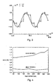
- Figure 3 shows a simulated response of the circuit of figure 1.
- Figure 4 shows simulated errors versus input currents according to the invention.
- the proposed new technique utilizes a composite transistor consisting of an MOS transistor and a bipolar transistor.
- The-MOS transistor is in common-drain configuration and the bipolar transistors are in common-emitter configuration as shown in Fig. 1.
- Current sources JO 1, I0 2 and I1 3 provide bias currents for transistors M0 4, Q0 5 and Q1 6, respectively.
- a capacitor C0 7 represents all the capacitance at the gate of the transistor M0 and C1 8 represents all the capacitance at the source of the transistor M0.
- All the switches are controlled by a non-overlapping clock.
- switches S0 9 and S1 10 are closed, and S2 11 is open.
- the input current Iin 12 flows into the collector of the transistor Q0 and makes the base-emitter voltage change correspondingly.
- Due to the common-drain configuration of the transistor M0 its gate source voltage does not change, the potential at the gate of the transistor M0 changes proportionally as well.
- a potential at the gate of the transistor M0 is created to change the base-emitter voltage of the transistor Q0 to sink (or source) the input current into the transistor Q0. Since the transistors Q0 and Q1 have the same base-emitter voltage, the output current Io1 14 is equal to the input current Iin, if the two transistors have the same emitter area.
- the switches S0 and S1 are open and S2 is closed.
- the gate of the MOS transistor M0 is isolated and the potential at the gate is held. Since the gate source voltage of the transistor M0 is constant, the base-emitter voltage of the transistor Q0 does not change. Therefore, the collector current of the Q0 does not change.
- the output current Io0 13 is equal to the input current Iin, that was the input into the transistor Q0 during the clock phase Ph0. Since the transistors Q0 and Q1 have the same base-emitter voltage, the output current Io1 is equal to the output current Io0, if the two transistors have the same emitter area.
- the output current Io0 is the memory of the input current Iin and the output current Io1 realizes the track-and-hold function performed on the input current Iin. Since same devices as M0 and Q0 are used both as input and as output devices, there is no mismatch between input current Iin and the output current Io0, just as in a second-generation SI memory cell. A scaling factor between the output current Io1 and the input current Iin can be realized by choosing a different emitter area.
- the speed of the circuit is determined by the settling time when the switches S0 and S1 are closed. Neglecting the switch-on resistance of the switch transistors, the system is a two-pole system.
- the dominant pole frequency ⁇ o is equal to g mQ0 /C0, where g mQ0 is the transconductance of the bipolar transistor Q0 and C0 is the total capacitance at the gate of M0.
- the non-dominant pole frequency ⁇ n is equal to g mM0 /C1, where g mM0 is the transconductance of the MOS transistor M0 and C1 is the total capacitance at the source of the transistor M0.
- the dominant pole frequency is determined by the total capacitance seen by the gate of the MOS transistor and the transconductance of the MOS transistor. Due to the higher transconductance of bipolar transistor, the proposed technique has a superior speed performance if the non-dominant frequency is sufficiently high. This can be satisfied in circuit design by minimizing the capacitance at the source of M0, especially when a reasonably large capacitance C0 is used to reduce clock feedthrough errors.
- the devices M0 and Q0 are used both as input and as output devices as in second-generation SI memory cells in the CMOS process, mismatch does not introduce any error. However, in most cases current mirrors are needed to realize different coefficients as in the case of using transistor Q1 and mismatch plays an important role. Since the bipolar transistor matching is better than the MOS transistor matching, the proposed technique is also superior to the SI technique in CMOS process concerning accuracy.
- the circuit illustrated in Fig. 1 can function well without further elaboration.
- the SI circuits are simple in the CMOS process too.
- the errors due to the gate-drain parasitic capacitance relatively complex circuits and/or clocking are needed.
- the proposed technique does not require linear capacitors as the SI technique in the CMOS process.
- the new technique does not demand matching between a transresistor and transconductor and the circuit scheme is much simpler.
- FIG. 2 An alternative circuit realization is shown in Fig. 2. It bears resemblance to the first-generation SI memory cell in the CMOS process.
- Fig. 2 different devices are used for input and output.
- the transistors M0 15 and Q0 16 are used as input devices, and the -transistors M1 17 and Q1 18 are used as output devices.
- Current sources J0 19, I0 20, J1 21 and I1 22 provide bias currents, for transistors M0, Q0, M1 and Q1, respectively.
- the capacitor C0 26 represents all the capacitance at the gate of transistor M0.
- the capacitor C1 27 represents all the capacitance at the source of transistor M0.
- the capacitor C2 28 represents all the capacitance at the gate of transistor M1.
- the capacitor C3 29 represents all the capacitance at the source of transistor M1.
- the transistors M0 and M1 have the same size and the transistors Q0 and Q1 have the same size.
- the gate voltage of the M1 is equal to that of the M0 and therefore the base emitter voltages of the transistors Q0 and Q1 equal.
- the collector currents of the Q0 and Q1 equal. Therefore the output current Io 24 is equal to the input current Iin 25.
- the gate of M1 is isolated and the potential is held. This makes the base-emitter voltage of the Q1 constant and therefore the collector current is constant.
- the output current Io is held constant. Therefore, the circuit realizes a track-and-hold function just as the first-generation SI memory cell in CMOS process. This circuit shows superior performance over its CMOS counterparts just as outlined above.
- Fig. 1 In order to verify the functionality, the circuit shown in Fig. 1 is simulated by using parameters of a 3.3-V digital BiCMOS process.
- the supply voltage is 3.3 V.
- the input current Iin and output current Io1 are shown in Fig. 3.
- the input current is a 20-MHz 100-uA sinusoidal and the clock frequency is 100 MHZ. It is evident that a track-and-hold function is realized.
- Fig. 4 the simulated current errors are shown versus input currents of a fully differential design based on the circuit scheme shown in Fig. 1.
- the bias current in each branch is about 360 uA. It is seen that when the sampling frequency is 100 Mhz, the error is less 0.55% and the variation is small. This indicates good linearity. When the clock frequency increases to 250 MHz, the error increases due to the settling error. The error variation is still small when the input current is less than 50% of the bias current, indicating good linearity.
Landscapes
- Metal-Oxide And Bipolar Metal-Oxide Semiconductor Integrated Circuits (AREA)
- Logic Circuits (AREA)
- Analogue/Digital Conversion (AREA)
- Bipolar Transistors (AREA)
- Amplifiers (AREA)
- Static Random-Access Memory (AREA)
Claims (2)
- Vorrichtung zum Verarbeiten abgetasteter analoger Signale in einem digitalen BiCMOS-Prozess unter Verwendung von MOS-Transistoren und Bipolartransistoren beim BiCMOS-Prozess, wobei Einrichtungen zum temporären Speichern einer Spannung am Gateanschluss eines MOS-Transistors vorgesehen sind, und wobei Einrichtungen zum Erhöhen der Geschwindigkeit vorgesehen sind, während eine Transkonduktanz eines Bipolartransistors verwendet wird, dadurch gekennzeichnet, dass ein MOS-Transistor (4) in einer Konfiguration mit gemeinsamem Drainanschluss und ein Bipolartransistor (5) in einer Konfiguration mit gemeinsamem Emitteranschluss beide als Eingangs- und Ausgangsvorrichtungen bei unterschiedlichen Taktphasen verwendet und angeschlossen sind, die durch einen sich nicht überlagernden Takt gesteuert sind, und dadurch, dass ein zusätzlicher Bipolartransistor (6) verwendet und angeschlossen ist, um eine Verfolgungs-und-Halte-Funktion mit einem möglichen Skalierungsfaktor zu realisieren, der durch die Emitterbereiche der zwei Bestandteils-Bipolartransistoren (5, 6) bestimmt ist.
- Vorrichtung nach Anspruch 1, dadurch gekennzeichnet, dass ein MOS-Transistor (15) in einer Konfiguration mit gemeinsamem Drainanschluss und ein Bipolartransistor (16) in einer Konfiguration mit gemeinsamem Emitteranschluss als die Eingangsvorrichtung verwendet und angeschlossen sind, dass ein weiterer MOS-Transistor (17) in einer Konfiguration mit gemeinsamem Drainanschluss und ein weiterer Bipolartransistor (18) in einer Konfiguration mit gemeinsamem Emitteranschluss als die Ausgangsvorrichtung verwendet und angeschlossen sind, und dass die Eingangs- und Ausgangsvorrichtungen nur bei einer Taktphase miteinander verbunden sind, die durch einen sich nicht überlagernden Takt gesteuert ist.
Applications Claiming Priority (3)
| Application Number | Priority Date | Filing Date | Title |
|---|---|---|---|
| SE9602362A SE517684C2 (sv) | 1996-06-14 | 1996-06-14 | Förfarande och anordning för att bearbeta samplade analoga signaler i en digital BiCMOS-process |
| SE9602362 | 1996-06-14 | ||
| PCT/SE1997/000979 WO1997048102A1 (en) | 1996-06-14 | 1997-06-04 | A METHOD AND DEVICE FOR PROCESSING SAMPLED ANALOGUE SIGNALS IN DIGITAL BiCMOS PROCESS |
Publications (2)
| Publication Number | Publication Date |
|---|---|
| EP0904590A1 EP0904590A1 (de) | 1999-03-31 |
| EP0904590B1 true EP0904590B1 (de) | 2002-08-28 |
Family
ID=20403013
Family Applications (1)
| Application Number | Title | Priority Date | Filing Date |
|---|---|---|---|
| EP97928571A Expired - Lifetime EP0904590B1 (de) | 1996-06-14 | 1997-06-04 | VORRICHTUNG ZUR VERARBEITUNG VON ABGETASTETEN ANALOGEN SIGNALEN INDIGITALEN BiCMOS-VERFAHREN |
Country Status (10)
| Country | Link |
|---|---|
| US (1) | US6091278A (de) |
| EP (1) | EP0904590B1 (de) |
| JP (1) | JP2000512055A (de) |
| CN (1) | CN1115695C (de) |
| AU (1) | AU3279797A (de) |
| CA (1) | CA2257900C (de) |
| DE (1) | DE69714993D1 (de) |
| SE (1) | SE517684C2 (de) |
| TW (1) | TW338841B (de) |
| WO (1) | WO1997048102A1 (de) |
Families Citing this family (6)
| Publication number | Priority date | Publication date | Assignee | Title |
|---|---|---|---|---|
| JP2005252816A (ja) * | 2004-03-05 | 2005-09-15 | Sanyo Electric Co Ltd | サンプルホールド回路 |
| US7911891B2 (en) * | 2006-06-05 | 2011-03-22 | Mediatek Inc. | Apparatus for controling servo signal gains of an optical disc drive and method of same |
| US8035416B1 (en) * | 2009-07-07 | 2011-10-11 | Contour Semiconductor, Inc. | Bipolar-MOS driver circuit |
| US9007801B2 (en) | 2009-07-07 | 2015-04-14 | Contour Semiconductor, Inc. | Bipolar-MOS memory circuit |
| TWI483903B (zh) * | 2011-05-27 | 2015-05-11 | Chun Lien Chuang | 改變生理食鹽水離子結構之裝置 |
| BR112014010838A8 (pt) * | 2011-11-11 | 2017-06-20 | Nec Corp | dispositivo de transmissão sem fio, método de encaminhamento de informação de falha e método de notificação de informação de falha |
Family Cites Families (3)
| Publication number | Priority date | Publication date | Assignee | Title |
|---|---|---|---|---|
| GB2225910A (en) * | 1988-12-08 | 1990-06-13 | Philips Electronic Associated | Processing sampled analogue electrical signals |
| JPH0420121A (ja) * | 1990-05-15 | 1992-01-23 | Fujitsu Ltd | Bi―CMOS回路 |
| JPH0669782A (ja) * | 1992-05-29 | 1994-03-11 | Nec Corp | BiMIS論理回路 |
-
1996
- 1996-06-14 SE SE9602362A patent/SE517684C2/sv not_active IP Right Cessation
-
1997
- 1997-06-04 CA CA002257900A patent/CA2257900C/en not_active Expired - Fee Related
- 1997-06-04 AU AU32797/97A patent/AU3279797A/en not_active Abandoned
- 1997-06-04 CN CN97195377A patent/CN1115695C/zh not_active Expired - Fee Related
- 1997-06-04 EP EP97928571A patent/EP0904590B1/de not_active Expired - Lifetime
- 1997-06-04 JP JP10501509A patent/JP2000512055A/ja active Pending
- 1997-06-04 DE DE69714993T patent/DE69714993D1/de not_active Expired - Lifetime
- 1997-06-04 WO PCT/SE1997/000979 patent/WO1997048102A1/en not_active Ceased
- 1997-06-13 US US08/876,050 patent/US6091278A/en not_active Expired - Lifetime
- 1997-06-19 TW TW086108602A patent/TW338841B/zh not_active IP Right Cessation
Also Published As
| Publication number | Publication date |
|---|---|
| US6091278A (en) | 2000-07-18 |
| CA2257900A1 (en) | 1997-12-18 |
| DE69714993D1 (de) | 2002-10-02 |
| HK1021245A1 (en) | 2000-06-02 |
| SE517684C2 (sv) | 2002-07-02 |
| EP0904590A1 (de) | 1999-03-31 |
| SE9602362L (sv) | 1997-12-15 |
| TW338841B (en) | 1998-08-21 |
| SE9602362D0 (sv) | 1996-06-14 |
| CN1115695C (zh) | 2003-07-23 |
| AU3279797A (en) | 1998-01-07 |
| JP2000512055A (ja) | 2000-09-12 |
| CA2257900C (en) | 2004-10-12 |
| WO1997048102A1 (en) | 1997-12-18 |
| CN1221512A (zh) | 1999-06-30 |
Similar Documents
| Publication | Publication Date | Title |
|---|---|---|
| EP0698236B1 (de) | Referenzschaltung mit kontrollierter temperaturabhängigkeit | |
| JP3120182B2 (ja) | 半導体集積回路 | |
| CA1178338A (en) | Switched capacitor temperature independent bandgap reference | |
| US5172019A (en) | Bootstrapped FET sampling switch | |
| US4484089A (en) | Switched-capacitor conductance-control of variable transconductance elements | |
| US5021692A (en) | Integrator circuit | |
| US4323796A (en) | Low transient feedthru FET sample and hold gate | |
| JPH06236697A (ja) | アナログ電流メモリ装置 | |
| EP0904590B1 (de) | VORRICHTUNG ZUR VERARBEITUNG VON ABGETASTETEN ANALOGEN SIGNALEN INDIGITALEN BiCMOS-VERFAHREN | |
| KR0161512B1 (ko) | 적분기 회로 | |
| JPS6225510A (ja) | 電流切換え回路 | |
| US5028822A (en) | Circuit arrangement for processing analogue electrical signals | |
| JP2707471B2 (ja) | 集積回路用のサンプルホールド増幅器 | |
| KR100467664B1 (ko) | 디지털BiCMOS프로세스에서의샘플링아날로그신호처리장치및방법 | |
| CN1108658C (zh) | 一种用于在数字cmos工艺中进行连续时间滤波的器件 | |
| KR860000906B1 (ko) | 샘플회로 | |
| HK1021245B (en) | A device for processing sampled analogue signals | |
| EP0669718A1 (de) | Elektronischer Schalter für integrierte MOS-Schaltungen mit niedriger Versorgungsspannung | |
| Huang et al. | Simple low-voltage high-speed high-linearity VI converter with S/H for analog signal processing applications | |
| JP4620678B2 (ja) | 特にアナログ/デジタルコンバータ用の差動サンプルホルダー | |
| JP2948931B2 (ja) | 電流分割器 | |
| Cujec et al. | An optimized bit cell design for a pipelined current-mode algorithmic A/D converter | |
| Romanczyk et al. | BiCMOS circuits for high speed current mode D/A converters | |
| JPH10508412A (ja) | 電流メモリ | |
| JP2782350B2 (ja) | 低歪電流源 |
Legal Events
| Date | Code | Title | Description |
|---|---|---|---|
| PUAI | Public reference made under article 153(3) epc to a published international application that has entered the european phase |
Free format text: ORIGINAL CODE: 0009012 |
|
| 17P | Request for examination filed |
Effective date: 19990114 |
|
| AK | Designated contracting states |
Kind code of ref document: A1 Designated state(s): DE ES FI FR GB IT NL SE |
|
| GRAG | Despatch of communication of intention to grant |
Free format text: ORIGINAL CODE: EPIDOS AGRA |
|
| RTI1 | Title (correction) |
Free format text: A DEVICE FOR PROCESSING SAMPLED ANALOGUE SIGNALS IN DIGITAL BICMOS PROCESS |
|
| GRAG | Despatch of communication of intention to grant |
Free format text: ORIGINAL CODE: EPIDOS AGRA |
|
| GRAH | Despatch of communication of intention to grant a patent |
Free format text: ORIGINAL CODE: EPIDOS IGRA |
|
| 17Q | First examination report despatched |
Effective date: 20011213 |
|
| GRAH | Despatch of communication of intention to grant a patent |
Free format text: ORIGINAL CODE: EPIDOS IGRA |
|
| GRAA | (expected) grant |
Free format text: ORIGINAL CODE: 0009210 |
|
| AK | Designated contracting states |
Kind code of ref document: B1 Designated state(s): DE ES FI FR GB IT NL SE |
|
| PG25 | Lapsed in a contracting state [announced via postgrant information from national office to epo] |
Ref country code: NL Free format text: LAPSE BECAUSE OF FAILURE TO SUBMIT A TRANSLATION OF THE DESCRIPTION OR TO PAY THE FEE WITHIN THE PRESCRIBED TIME-LIMIT Effective date: 20020828 Ref country code: IT Free format text: LAPSE BECAUSE OF FAILURE TO SUBMIT A TRANSLATION OF THE DESCRIPTION OR TO PAY THE FEE WITHIN THE PRESCRIBED TIME-LIMIT;WARNING: LAPSES OF ITALIAN PATENTS WITH EFFECTIVE DATE BEFORE 2007 MAY HAVE OCCURRED AT ANY TIME BEFORE 2007. THE CORRECT EFFECTIVE DATE MAY BE DIFFERENT FROM THE ONE RECORDED. Effective date: 20020828 Ref country code: FR Free format text: LAPSE BECAUSE OF NON-PAYMENT OF DUE FEES Effective date: 20020828 Ref country code: FI Free format text: LAPSE BECAUSE OF FAILURE TO SUBMIT A TRANSLATION OF THE DESCRIPTION OR TO PAY THE FEE WITHIN THE PRESCRIBED TIME-LIMIT Effective date: 20020828 |
|
| REG | Reference to a national code |
Ref country code: GB Ref legal event code: FG4D |
|
| REF | Corresponds to: |
Ref document number: 69714993 Country of ref document: DE Date of ref document: 20021002 |
|
| PG25 | Lapsed in a contracting state [announced via postgrant information from national office to epo] |
Ref country code: SE Free format text: LAPSE BECAUSE OF FAILURE TO SUBMIT A TRANSLATION OF THE DESCRIPTION OR TO PAY THE FEE WITHIN THE PRESCRIBED TIME-LIMIT Effective date: 20021128 |
|
| PG25 | Lapsed in a contracting state [announced via postgrant information from national office to epo] |
Ref country code: DE Free format text: LAPSE BECAUSE OF FAILURE TO SUBMIT A TRANSLATION OF THE DESCRIPTION OR TO PAY THE FEE WITHIN THE PRESCRIBED TIME-LIMIT Effective date: 20021129 |
|
| NLV1 | Nl: lapsed or annulled due to failure to fulfill the requirements of art. 29p and 29m of the patents act | ||
| PG25 | Lapsed in a contracting state [announced via postgrant information from national office to epo] |
Ref country code: ES Free format text: LAPSE BECAUSE OF FAILURE TO SUBMIT A TRANSLATION OF THE DESCRIPTION OR TO PAY THE FEE WITHIN THE PRESCRIBED TIME-LIMIT Effective date: 20030228 |
|
| EN | Fr: translation not filed | ||
| PLBE | No opposition filed within time limit |
Free format text: ORIGINAL CODE: 0009261 |
|
| STAA | Information on the status of an ep patent application or granted ep patent |
Free format text: STATUS: NO OPPOSITION FILED WITHIN TIME LIMIT |
|
| 26N | No opposition filed |
Effective date: 20030530 |
|
| PGFP | Annual fee paid to national office [announced via postgrant information from national office to epo] |
Ref country code: GB Payment date: 20080627 Year of fee payment: 12 |
|
| GBPC | Gb: european patent ceased through non-payment of renewal fee |
Effective date: 20090604 |
|
| PG25 | Lapsed in a contracting state [announced via postgrant information from national office to epo] |
Ref country code: GB Free format text: LAPSE BECAUSE OF NON-PAYMENT OF DUE FEES Effective date: 20090604 |