EP0903936A2 - Circuit séparateur de signaux de synchronisation - Google Patents
Circuit séparateur de signaux de synchronisation Download PDFInfo
- Publication number
- EP0903936A2 EP0903936A2 EP98307524A EP98307524A EP0903936A2 EP 0903936 A2 EP0903936 A2 EP 0903936A2 EP 98307524 A EP98307524 A EP 98307524A EP 98307524 A EP98307524 A EP 98307524A EP 0903936 A2 EP0903936 A2 EP 0903936A2
- Authority
- EP
- European Patent Office
- Prior art keywords
- level
- video signal
- sync
- signal
- counter
- Prior art date
- Legal status (The legal status is an assumption and is not a legal conclusion. Google has not performed a legal analysis and makes no representation as to the accuracy of the status listed.)
- Granted
Links
Images


Classifications
-
- H—ELECTRICITY
- H04—ELECTRIC COMMUNICATION TECHNIQUE
- H04N—PICTORIAL COMMUNICATION, e.g. TELEVISION
- H04N5/00—Details of television systems
- H04N5/04—Synchronising
- H04N5/08—Separation of synchronising signals from picture signals
Definitions
- the invention relates to a sync separating circuit for extracting a sync signal of a video signal and, more particularly, to a sync separating circuit to extract a sync signal from a digital video signal.
- a video signal is clamped, the clamped video signal is sliced by a predetermined level, and a sync signal is separated by the amplitude separation (for example, JP-A-6-253170).
- a video signal is supplied to an input terminal 51.
- the video signal from the input terminal 51 is supplied to a clamping circuit 52.
- the video signal is clamped so that, for example, a sync chip level of the video signal is made constant.
- An output of the clamping circuit 52 is supplied to a slice circuit 53.
- a level that is slightly higher than the sync chip level of the video signal is set as a slice level th into the slice circuit 53.
- the level of the video signal is compared with the slice level th.
- the output level of the clamping circuit 52 is higher than the threshold level th. In a period of time of the sync signal, the output level of the clamping circuit 52 is lower than the threshold level th.
- the sync signal can be extracted from the inputted video signal.
- the sync signal which is outputted from the slice circuit 53 is taken out from an output terminal 54.
- a video signal processing circuit is digitized and arranged on an integrated circuit.
- a circuit for directly digitizing the video signal and separating a sync signal from the digital video signal is considered.
- the sync chip level of the video signal is clamped and sliced by a slice level that is slightly higher than the sync chip level, so that the sync signal can be separated.
- the sync chip level fluctuates, it is difficult to accurately extract the sync signal.
- a minimum value S1 of the video signal is detected and a slice level formed on the basis of the minimum value S1 of the video signal is compared with the video signal, thereby extracting the sync signal. Since the sync chip level of the sync signal is equal to the minimum value of the video signal, if the minimum value of the video signal is detected and the slice level is formed as mentioned above, the slice level can be set to a level that is slightly higher than the sync chip level of the sync signal. Thus, the sync signal can be extracted.
- a noise N which drops to a low level is generated in the video signal.
- the slice level is formed on the basis of a minimum value S2 of the video signal, the slice level is equal to or less than the sync chip level due to an influence by the noise N which drops lower as mentioned above, so that a problem such that the sync signal cannot be extracted from the video signal occurs.
- a sync separating circuit comprising: holding means for holding a level based on a sync chip level; detecting means for comparing the slice level held in the holding means with a minimum value of a present video signal and outputting a detection signal when the minimum value of the present video signal is lower than the level held in the holding means; updating means for updating the level in the holding means on the basis of the minimum value of the present video signal when it is detected by the detecting means that the minimum value of the present video signal is lower than the level held in the holding means; and slice means for setting a slice level on the basis of the level in the holding means, slicing the video signal, and extracting a sync signal, wherein the slice level is allowed to gradually approach the sync chip level of the video signal by the updating means.
- the updating means updates the level in the holding means by an intermediate value between the level held in the holding means and the minimum value of the present video signal.
- the circuit further comprises mask means for inhibiting the updating of the level in the holding means for a predetermined time after the updating of the level in the holding means was executed for a predetermined period of time.
- the circuit further comprises level-up means for increasing the level held in the holding means at a predetermined rate is further provided.
- the sync signal separating circuit can certainly extract a sync signal from a digital video signal with less influence from noise as follows.
- the value held as a sync chip level may be compared with the minimum value of the present video signal and, when it is detected that the video signal at the present time point is lower than the holding level, it may be updated to a new level by the intermediate value between the level held so far and the minimum value of the video signal at that time. By a series of those operations, the holding level may be caused to gradually approach the sync chip level of the actual video signal.
- the sync signal can be certainly detected.
- the holding level By increasing the holding level at a predetermined rate, even if the signal level decreases to the sync chip level or less due to a sag, the holding level gradually approaches the sync chip level.
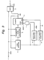
- Fig. 3 shows an example of a sync separating circuit to which the invention is applied.
- a digital video signal is supplied to an input terminal 1.
- the digital video signal from the input terminal 1 is supplied to a slice circuit 2.
- the slice circuit 2 is a comparator for comparing a signal level of the input video signal with a slice level that is slightly higher than a sync chip level of the video signal and extracting a sync signal.
- an output of an up-counter 3 is used as a slice level to be compared with the input video signal level.
- a value of the up-counter 3 gradually approaches the sync chip level of the video signal level.
- the slice level that is slightly higher than the sync chip level is set.
- the input video signal level is higher than the value of the up-counter 3.
- the sync signal is extracted from an output of the slice circuit 2.
- the sync signal extracted as mentioned above is outputted from an output terminal 4.
- a level detecting circuit 5 To allow the value of the up-counter 3 to gradually approach the sync chip level of the video signal level, a level detecting circuit 5, an intermediate value calculating circuit 6, an AND gate 7, a count enable pulse generating circuit 8, and a mask signal generating circuit 9 are provided.
- the digital video signal from the input terminal 1 is supplied to the level detecting circuit 5 and to the intermediate value calculating circuit 6.
- a value of the up-counter 3 is supplied to the level detecting circuit 5 and intermediate value calculating circuit 6.
- the level detecting circuit 5 compares the value of the up-counter 3 with the level of the input video signal and generates a detection signal when the value of the input video signal level is lower. For example, at the sync chip level of the sync signal, the input video signal level is lower than the value of the up-counter 3 and a detection output is derived from the level detecting circuit 5.
- the output of the level detecting circuit 5 is supplied to the AND gate 7 and is also supplied to the count enable pulse generating circuit 8 and mask signal generating circuit 9.
- the mask signal generating circuit 9 When it is detected by the level detecting circuit 5 that the video signal level is lower, the mask signal generating circuit 9 generates a mask signal of a low level for a predetermined period of time after the elapse of a predetermined period.
- the mask signal is provided to mask a noise when the noise which drops to a low level is generated in the video signal.
- the mask signal is supplied to the AND gate 7.
- the intermediate value calculating circuit 6 obtains an intermediate value between the value of the up-counter 3 and the input video signal level.
- the intermediate value is supplied as a preset value to the up-counter 3.
- a detection signal is outputted.
- a preset pulse is generated from the AND gate 7.
- the value of the intermediate value calculating circuit 6 is preset into the up-counter 3.
- the input video signal level is lower than the value of the up-counter 3 and the detection output is obtained from the level detecting circuit 5.
- the preset pulse is generated from the AND gate 7.
- the value of the intermediate value calculating circuit 6 is preset into the up-counter 3.
- the value of the intermediate value calculating circuit 6 in this instance is equal to the intermediate value between the value of the up-counter 3 so far and the sync chip level of the sync signal. Therefore, the value of the up-counter 3 gradually approaches the sync chip level of the sync signal.
- the mask signal from the mask signal generating circuit 9 is set to the low level for a predetermined period of time.
- the noise of the low level which is generated for the video period of time in the next horizontal period of time is masked.
- a count enable pulse is generated from the count enable pulse generating circuit 8 after the elapse of a predetermined period of time.
- the up-counter 3 is counted up.
- the up-counter 3 is counted up, even if a sag or the like occurs, the value of the up-counter 3 traces so as to approach the sync chip level.
- Figs. 4A to 4E show the operation of each section of the sync detecting circuit. It is now assumed that a video signal VIDEO as shown in Fig. 4A is supplied to the input terminal 1 in Fig. 3.
- the video signal includes a noise N1 which drops to the low level in the video period.
- the sync signal includes a noise N2 which drops to the low level.
- CNT denotes a value of the up-counter 3.
- the value CNT of the up-counter 3 gradually approaches the sync chip level of the sync signal of the video signal VIDEO.
- a preset pulse PRSET is generated from the AND gate 7.
- the value of the intermediate value calculating circuit 6 is preset into the up-counter 3.
- the value of the up-counter 3 decreases and approaches the sync chip level of the video signal VIDEO.
- an output of the mask signal generating circuit 9 is set to the low level for a period of time T mask from time point t 2 to time point t 4 .
- a count enable pulse EN is generated at time point t 3 .
- the count enable pulse as shown in Fig. 4A, the value CNT of the up-counter 3 is counted up.
- the noise N1 which drops to the low level exists in the video period, for the period of time when the noise N1 is generated, as shown in Fig. 2C, the output of the mask signal generating circuit 9 is at the low level. Therefore, the signal is not influenced by the noise N1 as mentioned above.
- the output of the mask signal generating circuit 9 is set to the high level.
- the video signal VIDEO is lower than the value CNT of the up-counter 3.
- the detection output appears from the level detecting circuit 5.
- the preset pulse PRSET is generated from the AND gate 7.
- the preset pulse PRSET the value of the intermediate value calculating circuit 6 is preset into the up-counter 3.
- the output of the mask signal generating circuit 9 is set to the low level for the period of time T mask from time point t 6 to time point t 8 .
- the count enable pulse EN is generated at time point t 7 .
- the value CNT of the up-counter 3 is preset to the intermediate value between the value of the up-counter 3 so far and the level of the noise N2. In this instance, there is a possibility such that the value CNT of the up-counter 3 is equal to or less than the sync chip level. However, since the value CNT of the up-counter 3 is counted up at time point t 7 , even if the value of the value CNT of the up-counter 3 decreases to the sync chip level or less, it gradually approaches the sync chip level after that.
- the value of the up-counter 3 with the presetting function gradually approaches the sync chip level irrespective of the noise N1 in the video period or the noise N2 in the sync signal period.
- the slice level set on the basis of the value of the up-counter 3 which gradually approaches the sync chip level is compared with the input video signal and the sync signal is extracted.
- the sync signal SYNC can be accurately extracted without being influenced by the noise.
- the sync chip level detected as mentioned above can be used as a reference of the clamping level without being limiting to only the extraction of the sync signal.
- the value held as a sync chip level is compared with the minimum value of the present video signal.
- the holding level is allowed to gradually approach the sync chip level of the video signal.
- the holding level By inhibiting the updating of the level for a predetermined time after the holding level was updated for a predetermined period of time, the influence by the noise in the video period of time is eliminated.
- the holding level By increasing the holding level at a predetermined rate, even if the slice level decreases to the sync chip level or less by the sag, the holding level gradually approaches the sync chip level.
- the sync chip level of the actual video signal can be detected, the sync signal can be certainly extracted from the digital video signal without being influenced by the noise.
- the sync chip level detected as mentioned above can be used as a reference of clamping without being limiting to only the extraction of the sync signal.
Landscapes
- Engineering & Computer Science (AREA)
- Multimedia (AREA)
- Signal Processing (AREA)
- Synchronizing For Television (AREA)
- Television Signal Processing For Recording (AREA)
- Picture Signal Circuits (AREA)
Applications Claiming Priority (3)
| Application Number | Priority Date | Filing Date | Title |
|---|---|---|---|
| JP252005/97 | 1997-09-17 | ||
| JP25200597 | 1997-09-17 | ||
| JP9252005A JPH1198382A (ja) | 1997-09-17 | 1997-09-17 | 同期分離回路 |
Publications (3)
| Publication Number | Publication Date |
|---|---|
| EP0903936A2 true EP0903936A2 (fr) | 1999-03-24 |
| EP0903936A3 EP0903936A3 (fr) | 2000-10-18 |
| EP0903936B1 EP0903936B1 (fr) | 2006-05-31 |
Family
ID=17231249
Family Applications (1)
| Application Number | Title | Priority Date | Filing Date |
|---|---|---|---|
| EP98307524A Expired - Lifetime EP0903936B1 (fr) | 1997-09-17 | 1998-09-16 | Circuit séparateur de signaux de synchronisation |
Country Status (4)
| Country | Link |
|---|---|
| US (1) | US6259485B1 (fr) |
| EP (1) | EP0903936B1 (fr) |
| JP (1) | JPH1198382A (fr) |
| DE (1) | DE69834696T2 (fr) |
Cited By (1)
| Publication number | Priority date | Publication date | Assignee | Title |
|---|---|---|---|---|
| TWI419571B (zh) * | 2009-07-03 | 2013-12-11 | Acer Inc | Effective display cycle judgment device and its judgment method, resolution judgment system and judgment method thereof |
Families Citing this family (4)
| Publication number | Priority date | Publication date | Assignee | Title |
|---|---|---|---|---|
| US6882360B2 (en) * | 2001-09-05 | 2005-04-19 | General Instrument Corporation | Method and apparatus for determining a level of a video signal |
| JP2007288260A (ja) * | 2006-04-12 | 2007-11-01 | Matsushita Electric Ind Co Ltd | Vbiデータスライス回路 |
| JP5237606B2 (ja) * | 2007-10-10 | 2013-07-17 | セミコンダクター・コンポーネンツ・インダストリーズ・リミテッド・ライアビリティ・カンパニー | 同期分離回路 |
| TW200945909A (en) * | 2008-04-22 | 2009-11-01 | Novatek Microelectronics Corp | Synchronization signal extraction device and related method |
Family Cites Families (16)
| Publication number | Priority date | Publication date | Assignee | Title |
|---|---|---|---|---|
| US4185299A (en) * | 1978-08-18 | 1980-01-22 | Rca Corporation | Synchronization signal separator circuit |
| JPS5672581A (en) * | 1979-11-16 | 1981-06-16 | Matsushita Electric Ind Co Ltd | Synchronizing signal separator |
| US4357629A (en) * | 1980-12-29 | 1982-11-02 | Motorola, Inc. | Sync separator with variable bias control |
| JPS5892187A (ja) * | 1981-11-27 | 1983-06-01 | Pioneer Video Corp | 同期分離回路 |
| US4616270A (en) * | 1983-07-14 | 1986-10-07 | Victor Company Of Japan, Ltd. | Synchronizing signal separating circuit for a recording and reproducing apparatus |
| US4691248A (en) * | 1983-07-14 | 1987-09-01 | Victor Company Of Japan | Synchronized signal separating circuit for a recording and reproducing apparatus |
| US4707740A (en) * | 1986-04-11 | 1987-11-17 | Harris Corporation | Sync detector having noise adjusted slice level |
| US4723165A (en) * | 1986-11-26 | 1988-02-02 | Zenith Electronics Corporation | AC coupled sync separator system with filter DC feedback |
| DE4127120A1 (de) | 1991-08-16 | 1993-02-18 | Thomson Brandt Gmbh | Verfahren und einrichtung zur abtrennung des synchronisationssignals aus einem bildsignal |
| US5754250A (en) * | 1992-02-18 | 1998-05-19 | Cooper; J. Carl | Synchronizing signal separating apparatus and method |
| US5404172A (en) | 1992-03-02 | 1995-04-04 | Eeg Enterprises, Inc. | Video signal data and composite synchronization extraction circuit for on-screen display |
| JPH06253170A (ja) | 1993-02-26 | 1994-09-09 | Sony Corp | ビデオ信号処理回路 |
| US5528303A (en) * | 1993-11-01 | 1996-06-18 | Elantec, Inc. | Synchronizing signal active filter and method |
| US5486867A (en) | 1993-11-30 | 1996-01-23 | Raytheon Company | High resolution digital phase detector |
| KR0155615B1 (ko) * | 1995-07-27 | 1998-11-16 | 문정환 | 영상출력장치의 동기신호분리회로 |
| CA2157986A1 (fr) * | 1995-09-11 | 1997-03-12 | Gennum Corporation | Circuits d'extraction de signaux de synchronisation et de detection de signaux video |
-
1997
- 1997-09-17 JP JP9252005A patent/JPH1198382A/ja active Pending
-
1998
- 1998-09-15 US US09/153,353 patent/US6259485B1/en not_active Expired - Fee Related
- 1998-09-16 DE DE69834696T patent/DE69834696T2/de not_active Expired - Fee Related
- 1998-09-16 EP EP98307524A patent/EP0903936B1/fr not_active Expired - Lifetime
Cited By (1)
| Publication number | Priority date | Publication date | Assignee | Title |
|---|---|---|---|---|
| TWI419571B (zh) * | 2009-07-03 | 2013-12-11 | Acer Inc | Effective display cycle judgment device and its judgment method, resolution judgment system and judgment method thereof |
Also Published As
| Publication number | Publication date |
|---|---|
| EP0903936A3 (fr) | 2000-10-18 |
| DE69834696T2 (de) | 2007-05-03 |
| EP0903936B1 (fr) | 2006-05-31 |
| JPH1198382A (ja) | 1999-04-09 |
| DE69834696D1 (de) | 2006-07-06 |
| US6259485B1 (en) | 2001-07-10 |
Similar Documents
| Publication | Publication Date | Title |
|---|---|---|
| KR100307979B1 (ko) | 보조비디오데이타슬라이서 | |
| US5517249A (en) | Auxiliary video data slicer with adaptive slicing level capability | |
| US5463423A (en) | Auxiliary video data detector and data slicer | |
| WO1998001956A3 (fr) | Systeme servant a supprimer le bruit d'un micro | |
| US5392317A (en) | Method and apparatus extracting pulse signal | |
| EP0903936B1 (fr) | Circuit séparateur de signaux de synchronisation | |
| US6912009B2 (en) | Data slice circuit separating data added to a signal superposed on a video signal based on slice level | |
| EP0716539A2 (fr) | Séparateur de signal de synchronisation adaptatif | |
| GB2225190A (en) | Deriving horizontal and vertical sync pulses from a three-level HDTV sync signal | |
| US5467140A (en) | Vertical synchronous signal separation apparatus | |
| ATE98825T1 (de) | Verfahren zum einstellen elektronischer schaltungen. | |
| US5867222A (en) | Video sync signal slicing using variable gain control | |
| JP2520455B2 (ja) | 相関ピ―ク検出回路 | |
| JP3338726B2 (ja) | サージ識別装置 | |
| EP0828359A3 (fr) | Récepteur de signaux optiques en rafale et méthode de réception correspondante | |
| EP0164978A1 (fr) | Séparateur d'impulsions de synchronisation verticale | |
| KR20060084365A (ko) | 동기식 검출기 | |
| KR0170238B1 (ko) | 중간 주파수 신호처리용 자동이득 제어회로 | |
| JPS60248082A (ja) | 映像信号受信の有無検出回路 | |
| JPH04972A (ja) | 垂直同期分離回路 | |
| JPS6397069A (ja) | 同期分離回路 | |
| JP3064311B2 (ja) | バーストフラグ回路 | |
| JPS5990478A (ja) | デ−タスライス回路 | |
| JPH05227452A (ja) | 同期分離回路 | |
| JPS63153963A (ja) | 同期分離装置 |
Legal Events
| Date | Code | Title | Description |
|---|---|---|---|
| PUAI | Public reference made under article 153(3) epc to a published international application that has entered the european phase |
Free format text: ORIGINAL CODE: 0009012 |
|
| AK | Designated contracting states |
Kind code of ref document: A2 Designated state(s): DE GB NL |
|
| AX | Request for extension of the european patent |
Free format text: AL;LT;LV;MK;RO;SI |
|
| PUAL | Search report despatched |
Free format text: ORIGINAL CODE: 0009013 |
|
| AK | Designated contracting states |
Kind code of ref document: A3 Designated state(s): AT BE CH CY DE DK ES FI FR GB GR IE IT LI LU MC NL PT SE |
|
| AX | Request for extension of the european patent |
Free format text: AL;LT;LV;MK;RO;SI |
|
| 17P | Request for examination filed |
Effective date: 20010320 |
|
| AKX | Designation fees paid |
Free format text: DE GB NL |
|
| GRAP | Despatch of communication of intention to grant a patent |
Free format text: ORIGINAL CODE: EPIDOSNIGR1 |
|
| GRAS | Grant fee paid |
Free format text: ORIGINAL CODE: EPIDOSNIGR3 |
|
| GRAA | (expected) grant |
Free format text: ORIGINAL CODE: 0009210 |
|
| AK | Designated contracting states |
Kind code of ref document: B1 Designated state(s): DE GB NL |
|
| REG | Reference to a national code |
Ref country code: GB Ref legal event code: FG4D |
|
| REF | Corresponds to: |
Ref document number: 69834696 Country of ref document: DE Date of ref document: 20060706 Kind code of ref document: P |
|
| PLBE | No opposition filed within time limit |
Free format text: ORIGINAL CODE: 0009261 |
|
| STAA | Information on the status of an ep patent application or granted ep patent |
Free format text: STATUS: NO OPPOSITION FILED WITHIN TIME LIMIT |
|
| 26N | No opposition filed |
Effective date: 20070301 |
|
| PGFP | Annual fee paid to national office [announced via postgrant information from national office to epo] |
Ref country code: NL Payment date: 20080903 Year of fee payment: 11 |
|
| PGFP | Annual fee paid to national office [announced via postgrant information from national office to epo] |
Ref country code: GB Payment date: 20080917 Year of fee payment: 11 |
|
| PGFP | Annual fee paid to national office [announced via postgrant information from national office to epo] |
Ref country code: DE Payment date: 20081002 Year of fee payment: 11 |
|
| REG | Reference to a national code |
Ref country code: NL Ref legal event code: V1 Effective date: 20100401 |
|
| GBPC | Gb: european patent ceased through non-payment of renewal fee |
Effective date: 20090916 |
|
| PG25 | Lapsed in a contracting state [announced via postgrant information from national office to epo] |
Ref country code: NL Free format text: LAPSE BECAUSE OF NON-PAYMENT OF DUE FEES Effective date: 20100401 Ref country code: DE Free format text: LAPSE BECAUSE OF NON-PAYMENT OF DUE FEES Effective date: 20100401 |
|
| PG25 | Lapsed in a contracting state [announced via postgrant information from national office to epo] |
Ref country code: GB Free format text: LAPSE BECAUSE OF NON-PAYMENT OF DUE FEES Effective date: 20090916 |