EP0903847A1 - Circuit amplificateur - Google Patents
Circuit amplificateur Download PDFInfo
- Publication number
- EP0903847A1 EP0903847A1 EP98117672A EP98117672A EP0903847A1 EP 0903847 A1 EP0903847 A1 EP 0903847A1 EP 98117672 A EP98117672 A EP 98117672A EP 98117672 A EP98117672 A EP 98117672A EP 0903847 A1 EP0903847 A1 EP 0903847A1
- Authority
- EP
- European Patent Office
- Prior art keywords
- output terminal
- terminal
- amplifier circuit
- output
- input
- Prior art date
- Legal status (The legal status is an assumption and is not a legal conclusion. Google has not performed a legal analysis and makes no representation as to the accuracy of the status listed.)
- Granted
Links
- 239000003990 capacitor Substances 0.000 claims description 19
- 238000010586 diagram Methods 0.000 description 16
- 238000010276 construction Methods 0.000 description 13
- 230000008878 coupling Effects 0.000 description 11
- 238000010168 coupling process Methods 0.000 description 11
- 238000005859 coupling reaction Methods 0.000 description 11
- 230000009467 reduction Effects 0.000 description 3
- NAWXUBYGYWOOIX-SFHVURJKSA-N (2s)-2-[[4-[2-(2,4-diaminoquinazolin-6-yl)ethyl]benzoyl]amino]-4-methylidenepentanedioic acid Chemical compound C1=CC2=NC(N)=NC(N)=C2C=C1CCC1=CC=C(C(=O)N[C@@H](CC(=C)C(O)=O)C(O)=O)C=C1 NAWXUBYGYWOOIX-SFHVURJKSA-N 0.000 description 2
- 230000008859 change Effects 0.000 description 1
- 230000007423 decrease Effects 0.000 description 1
- 230000006872 improvement Effects 0.000 description 1
- 229910052710 silicon Inorganic materials 0.000 description 1
- 239000010703 silicon Substances 0.000 description 1
- 230000009466 transformation Effects 0.000 description 1
Images


Classifications
-
- H—ELECTRICITY
- H03—ELECTRONIC CIRCUITRY
- H03F—AMPLIFIERS
- H03F3/00—Amplifiers with only discharge tubes or only semiconductor devices as amplifying elements
- H03F3/34—DC amplifiers in which all stages are DC-coupled
- H03F3/343—DC amplifiers in which all stages are DC-coupled with semiconductor devices only
- H03F3/347—DC amplifiers in which all stages are DC-coupled with semiconductor devices only in integrated circuits
Definitions
- the present invention relates to an amplifier circuit for outputting an input signal at a specific output impedance, and in particular, to an amplifier circuit that is built in a video camera and the like and is used for amplifying a video signal and the like.
- the amplifier circuit since an output impedance is specified at 75 ohms in an amplifier circuit for outputting a video signal, the amplifier circuit outputs a signal through a resistor of 75 ohms by driving the signal in a low-impedance output amplifier circuit, the signal being twice as large as a signal at a 75-ohm terminating resistor.
- the conventional amplifier circuit it is necessary for the conventional amplifier circuit to output a signal of 2 Vpp in the low-impedance output amplifier circuit so as to output a video signal having an amplitude of 1 Vpp. Therefore, a supply voltage of at least 4 V is required if the low-impedance output amplifier circuit is constructed of a push-pull circuit with bipolar transistors.
- the low-impedance output amplifier circuit is constructed in a collector-output type, it is possible to lower the supply voltage to a degree. Nevertheless, it is difficult to operate the low-impedance output amplifier circuit at the supply voltage of 3 V.
- An object of the present invention is to provide an amplifier circuit which is operable at a supply voltage of 3 V.
- an amplifier circuit for amplifying an input signal and outputting the amplified signal which comprises a first amplifier for outputting from a first output terminal a current proportional to a difference voltage between voltages at a first input terminal and a second input terminal, and a second amplifier for outputting from a second output terminal a current proportional to a difference voltage between voltages at the first input terminal and the second input terminal and for feeding back a current outputted from the second output terminal to the second input terminal.
- Fig. 1 is a diagram showing the fundamental construction of an amplifier circuit according to the embodiment.
- reference numeral 1 denotes a first input terminal
- reference numeral 2 denotes an second input terminal
- reference numeral 3 denotes a first output terminal
- reference numeral 4 denotes a second output terminal
- reference numeral 5 denotes a first Gm amplifier for outputting a current to the first output terminal 3
- reference numeral 6 denotes a second Gm amplifier for outputting a current to the second output terminal 4.
- Fig. 2 is a diagram showing the construction of the amplifier circuit whose input terminal a signal source is connected to when the input-output gain is determined.
- reference numeral 7 denotes an input signal source
- reference numeral 8 denotes a terminating resistor
- reference numerals 9 and 10 denote feedback resistors.
- conductances (Gm's) of the first Gm amplifier 5 and the second Gm amplifier 6 be Gm1 and Gm2, respectively
- resistances of the terminating resistor 8 and the feedback resistors 9 and 10 be R, R1 and R2, respectively.
- the input-output gain is determined by deciding the respective values of the resistances R, R1, and R2 and the conductances Gm1 and Gm2.
- Fig. 3 is a diagram showing the construction of the amplifier circuit whose output terminal a signal source is connected to when an output impedance is determined.
- v1 (R1+R2+R1R2Gm2)/(R1+R2+R1R2Gm2+R(1+R2Gm1+R2Gm2)) ⁇ vin
- Fig. 4 is a diagram showing the structure of an amplifier circuit for outputting a signal through the capacitive coupling.
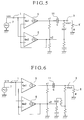
- Fig. 5 is a diagram showing the construction of the amplifier circuit having a feedback circuit for performing the feedback of the video signal after the capacitive coupling to the second input terminal.
- Fig. 6, similarly to Fig. 5, is a diagram showing the construction of the amplifier circuit having a feedback circuit for performing the feedback of the video signal after the capacitive coupling to the second input terminal.
- the feedback circuit shown in Fig. 5 is stable when there is not a terminating resistor, and the feedback circuit shown in Fig. 6 has a good frequency characteristic.
- Fig. 7 is a timing chart showing signal waveforms of the respective portions in the amplifier circuit shown in Fig. 5 or Fig. 6.
- a resistor and a capacitor are connected in series between the terminal of the output side of the capacitive coupling 11 and the second output terminal in Fig. 5, only the capacitor can be also connected.
- a resistor and a capacitor are connected in series between the connecting point of two resistors, connected in series between the terminal of the output side of the capacitive coupling 11 and the ground, and the second output terminal in Fig. 6, only the capacitor can be also connected.
- Fig. 8 is a diagram showing the concrete construction of the amplifier circuit shown in Fig. 1.
- the amplifier circuit has a bandgap circuit 12.
- a bandgap voltage generated in the bandgap circuit 12 is inputted to the base of an NPN transistor (Tr) 13, and an external resistor 14 is connected between the emitter of the NPN transistor 13 and the ground (GND).
- Fig. 9 is a diagram showing the principle of operation of the bandgap circuit 12.
- a bandgap circuit is a circuit for outputting a bandgap voltage (about 1.2 V) for silicon, and has a characteristic that is not fluctuated by temperature.
- a resistor Ra is connected to the emitter of a transistor having N times the size between two transistors having different sizes (1:N), and the same base potential is given to the two transistors so that the same collector currents may flow.
- Vbandgap Vbe+2 ⁇ (Rb/Ra) ⁇ (k ⁇ lnN/q) ⁇ T
- the collector current of the NPN transistor (Tr) 13 shown in Fig. 8 becomes proportional to the absolute temperature. Then, by making currents, mirrored from the collector current of the NPN transistor 13, flow into emitter-coupled differential input circuits 15 and 16, the emitter-coupled differential input circuits 15 and 16 can have conductances (Gm's) of a characteristic not depending on temperature.
- output currents from the emittercoupled differential input circuits 15 and 16 are mirrored by transistors 17 and 18, and are outputted to the second output terminal 4. Furthermore, the currents are mirrored by transistors 19 and 20, and are outputted to the first output terminal 3.
- the output impedance obtained from Fig. 3 small by putting conductances in Gm1>>Gm2, and, at this time, the output impedance becomes Z ⁇ R1(Gm2/Gm1).
- the resistance R1 is several-ten k ⁇
- the current outputted from the first output terminal is several-ten to several-hundred times larger than the current outputted from the second output terminal.
- the amplifier circuit since it is possible to adjust the output level at the time of termination by applying the feedback so that the output impedance may become 75 ⁇ , the amplifier circuit can operate at a supply voltage of 3 V if the signal amplitude of the first output terminal is 1 Vpp.
- the amplifier circuit of the present invention since it is possible to adjust the output level at the time of termination by applying the feedback so that the output impedance may become 75 ⁇ , the amplifier circuit can operate at a supply voltage of 3 V if the signal amplitude of the first output terminal is 1 Vpp, which is different from the output amplitude of 2 Vpp from a conventional video output amplifier circuit. Owing to this, it is possible to provide an amplifier circuit for video output that is operable at a supply voltage of 3 V. In this manner, since it is possible to use a supply voltage of 3 V in a portable apparatus such as a video camera, it is possible to achieve cost reduction by simplification of the construction of a power supply and performance improvement by lengthening continuous duty time of a battery.
- An amplifier circuit for amplifying an input signal and outputting the amplified signal includes a first amplifier for outputting from a first output terminal a current proportional to a difference voltage between voltages at a first input terminal and a second input terminal, and a second amplifier for outputting from a second output terminal a current proportional to a difference voltage between voltages at the first input terminal and the second input terminal and for feeding back a current outputted from the second output terminal to the second input terminal, so that the amplifier circuit is operable at a supply voltage of 3 V.
Landscapes
- Engineering & Computer Science (AREA)
- Microelectronics & Electronic Packaging (AREA)
- Power Engineering (AREA)
- Amplifiers (AREA)
- Picture Signal Circuits (AREA)
Applications Claiming Priority (3)
| Application Number | Priority Date | Filing Date | Title |
|---|---|---|---|
| JP270337/97 | 1997-09-18 | ||
| JP9270337A JPH1197954A (ja) | 1997-09-18 | 1997-09-18 | 増幅回路 |
| JP27033797 | 1997-09-18 |
Publications (2)
| Publication Number | Publication Date |
|---|---|
| EP0903847A1 true EP0903847A1 (fr) | 1999-03-24 |
| EP0903847B1 EP0903847B1 (fr) | 2004-03-17 |
Family
ID=17484856
Family Applications (1)
| Application Number | Title | Priority Date | Filing Date |
|---|---|---|---|
| EP98117672A Expired - Lifetime EP0903847B1 (fr) | 1997-09-18 | 1998-09-17 | Circuit amplificateur |
Country Status (4)
| Country | Link |
|---|---|
| US (1) | US6091294A (fr) |
| EP (1) | EP0903847B1 (fr) |
| JP (1) | JPH1197954A (fr) |
| DE (1) | DE69822389T2 (fr) |
Families Citing this family (5)
| Publication number | Priority date | Publication date | Assignee | Title |
|---|---|---|---|---|
| US6466089B2 (en) * | 2000-10-11 | 2002-10-15 | Texas Instruments Incorporated | Control circuit for increasing the output inpedance of a transconductor |
| JP4407881B2 (ja) | 2002-10-16 | 2010-02-03 | ローム株式会社 | バッファ回路及びドライバic |
| US6937099B2 (en) * | 2003-12-04 | 2005-08-30 | Analog Devices, Inc. | Op-amp configurable in a non-inverting mode with a closed loop gain greater than one with output voltage correction for a time varying voltage reference of the op-amp, and a method for correcting the output voltage of such an op-amp for a time varying voltage reference |
| KR100921515B1 (ko) | 2006-12-05 | 2009-10-15 | 한국전자통신연구원 | 간략화된 nauta 연산 상호 컨덕턴스 증폭기 |
| JP2008181812A (ja) | 2007-01-25 | 2008-08-07 | Toyota Motor Corp | 燃料電池製造装置及び燃料電池 |
Citations (1)
| Publication number | Priority date | Publication date | Assignee | Title |
|---|---|---|---|---|
| US4929909A (en) * | 1989-03-27 | 1990-05-29 | Analog Devices, Inc. | Differential amplifier with gain compensation |
Family Cites Families (3)
| Publication number | Priority date | Publication date | Assignee | Title |
|---|---|---|---|---|
| GB1204617A (en) * | 1968-04-10 | 1970-09-09 | Cossor Ltd A C | Circuit providing a floating output |
| US5027081A (en) * | 1990-05-03 | 1991-06-25 | Motorola, Inc. | High gain differential-to-single ended amplifier having a tee network feedback loop |
| TW239239B (fr) * | 1993-07-14 | 1995-01-21 | Philips Electronics Nv |
-
1997
- 1997-09-18 JP JP9270337A patent/JPH1197954A/ja active Pending
-
1998
- 1998-09-10 US US09/150,564 patent/US6091294A/en not_active Expired - Lifetime
- 1998-09-17 EP EP98117672A patent/EP0903847B1/fr not_active Expired - Lifetime
- 1998-09-17 DE DE69822389T patent/DE69822389T2/de not_active Expired - Lifetime
Patent Citations (1)
| Publication number | Priority date | Publication date | Assignee | Title |
|---|---|---|---|---|
| US4929909A (en) * | 1989-03-27 | 1990-05-29 | Analog Devices, Inc. | Differential amplifier with gain compensation |
Non-Patent Citations (3)
| Title |
|---|
| A.M. SOLIMAN: "Design of High-Frequency Amplifiers", IEEE CIRCUITS AND SYSTEMS MAGAZINE., vol. 5, no. 2, June 1983 (1983-06-01), NEW YORK US, pages 9 - 11, XP002087773 * |
| GRAEME J: "OP-AMP DISTORTION MEASUREMENT BYPASSES TEST-EQUIPMENT LIMITS DESIGNER'S GUIDE TO MEASURING OP-AMP DISTORTION PART 1", EDN ELECTRICAL DESIGN NEWS, vol. 37, no. 4, 17 February 1992 (1992-02-17), pages 133 - 136, XP000292859 * |
| HAIDEH KHORRAMABADI ET AL: "A HIGHLY EFFICIENT CMOS LINE DRIVER WITH 80-DB LINEARITY FOR ISDN U-INTERFACE APPLICATIONS", IEEE JOURNAL OF SOLID-STATE CIRCUITS, vol. 27, no. 12, 1 December 1992 (1992-12-01), pages 1723 - 1729, XP000329021 * |
Also Published As
| Publication number | Publication date |
|---|---|
| EP0903847B1 (fr) | 2004-03-17 |
| DE69822389D1 (de) | 2004-04-22 |
| JPH1197954A (ja) | 1999-04-09 |
| DE69822389T2 (de) | 2005-03-10 |
| US6091294A (en) | 2000-07-18 |
Similar Documents
| Publication | Publication Date | Title |
|---|---|---|
| EP0439071B1 (fr) | Amplificateur logarithmique | |
| US6091294A (en) | Amplifier circuit | |
| JP2774881B2 (ja) | ガンマ補正回路 | |
| EP0314218B1 (fr) | Circuit amplificateur et dispositif de reproduction muni de ce circuit amplificateur | |
| US6570427B2 (en) | Variable transconductance amplifier | |
| US4725790A (en) | Broadband DC level shift circuit with feedback | |
| US6313884B1 (en) | Gamma correction | |
| JPH0712128B2 (ja) | 増幅器 | |
| KR100375386B1 (ko) | 집적회로의웨이퍼단계온도보상 | |
| EP1676362B1 (fr) | Circuit electronique pour l'amplification d'un signal bipolaire | |
| JP3107590B2 (ja) | 電流極性変換回路 | |
| JP3509167B2 (ja) | カレントミラー装置 | |
| JP3216753B2 (ja) | D−a変換回路装置 | |
| JP3534275B2 (ja) | 電流源及び集積回路 | |
| JPH0527282B2 (fr) | ||
| JP2793194B2 (ja) | 定電流回路 | |
| JP3165173B2 (ja) | 静電容量センサ回路 | |
| JP3146088B2 (ja) | 可変リアクタンス回路 | |
| JP2853485B2 (ja) | 電圧電流変換回路 | |
| JP2722769B2 (ja) | 利得制御回路 | |
| JP2680748B2 (ja) | 結合容量回路 | |
| JP2693861B2 (ja) | 増幅回路 | |
| JPS59181802A (ja) | 電流入力型増幅装置 | |
| JPH01233813A (ja) | 可変利得増幅器 | |
| JP2000295051A (ja) | オフセット調整回路 |
Legal Events
| Date | Code | Title | Description |
|---|---|---|---|
| PUAI | Public reference made under article 153(3) epc to a published international application that has entered the european phase |
Free format text: ORIGINAL CODE: 0009012 |
|
| AK | Designated contracting states |
Kind code of ref document: A1 Designated state(s): DE FR GB NL |
|
| AX | Request for extension of the european patent |
Free format text: AL;LT;LV;MK;RO;SI |
|
| 17P | Request for examination filed |
Effective date: 19990811 |
|
| AKX | Designation fees paid |
Free format text: DE FR GB NL |
|
| 17Q | First examination report despatched |
Effective date: 20020819 |
|
| GRAP | Despatch of communication of intention to grant a patent |
Free format text: ORIGINAL CODE: EPIDOSNIGR1 |
|
| GRAS | Grant fee paid |
Free format text: ORIGINAL CODE: EPIDOSNIGR3 |
|
| GRAA | (expected) grant |
Free format text: ORIGINAL CODE: 0009210 |
|
| AK | Designated contracting states |
Kind code of ref document: B1 Designated state(s): DE FR GB NL |
|
| REG | Reference to a national code |
Ref country code: GB Ref legal event code: FG4D |
|
| REF | Corresponds to: |
Ref document number: 69822389 Country of ref document: DE Date of ref document: 20040422 Kind code of ref document: P |
|
| ET | Fr: translation filed | ||
| PLBE | No opposition filed within time limit |
Free format text: ORIGINAL CODE: 0009261 |
|
| STAA | Information on the status of an ep patent application or granted ep patent |
Free format text: STATUS: NO OPPOSITION FILED WITHIN TIME LIMIT |
|
| 26N | No opposition filed |
Effective date: 20041220 |
|
| PGFP | Annual fee paid to national office [announced via postgrant information from national office to epo] |
Ref country code: FR Payment date: 20111005 Year of fee payment: 14 |
|
| PGFP | Annual fee paid to national office [announced via postgrant information from national office to epo] |
Ref country code: NL Payment date: 20110923 Year of fee payment: 14 |
|
| REG | Reference to a national code |
Ref country code: NL Ref legal event code: V1 Effective date: 20130401 |
|
| REG | Reference to a national code |
Ref country code: FR Ref legal event code: ST Effective date: 20130531 |
|
| PG25 | Lapsed in a contracting state [announced via postgrant information from national office to epo] |
Ref country code: NL Free format text: LAPSE BECAUSE OF NON-PAYMENT OF DUE FEES Effective date: 20130401 Ref country code: FR Free format text: LAPSE BECAUSE OF NON-PAYMENT OF DUE FEES Effective date: 20121001 |
|
| PGFP | Annual fee paid to national office [announced via postgrant information from national office to epo] |
Ref country code: GB Payment date: 20150922 Year of fee payment: 18 Ref country code: DE Payment date: 20150930 Year of fee payment: 18 |
|
| REG | Reference to a national code |
Ref country code: DE Ref legal event code: R119 Ref document number: 69822389 Country of ref document: DE |
|
| GBPC | Gb: european patent ceased through non-payment of renewal fee |
Effective date: 20160917 |
|
| PG25 | Lapsed in a contracting state [announced via postgrant information from national office to epo] |
Ref country code: DE Free format text: LAPSE BECAUSE OF NON-PAYMENT OF DUE FEES Effective date: 20170401 Ref country code: GB Free format text: LAPSE BECAUSE OF NON-PAYMENT OF DUE FEES Effective date: 20160917 |