EP0903847A1 - Amplifier circuit - Google Patents
Amplifier circuit Download PDFInfo
- Publication number
- EP0903847A1 EP0903847A1 EP98117672A EP98117672A EP0903847A1 EP 0903847 A1 EP0903847 A1 EP 0903847A1 EP 98117672 A EP98117672 A EP 98117672A EP 98117672 A EP98117672 A EP 98117672A EP 0903847 A1 EP0903847 A1 EP 0903847A1
- Authority
- EP
- European Patent Office
- Prior art keywords
- output terminal
- terminal
- amplifier circuit
- output
- input
- Prior art date
- Legal status (The legal status is an assumption and is not a legal conclusion. Google has not performed a legal analysis and makes no representation as to the accuracy of the status listed.)
- Granted
Links
Images


Classifications
-
- H—ELECTRICITY
- H03—ELECTRONIC CIRCUITRY
- H03F—AMPLIFIERS
- H03F3/00—Amplifiers with only discharge tubes or only semiconductor devices as amplifying elements
- H03F3/34—Dc amplifiers in which all stages are dc-coupled
- H03F3/343—Dc amplifiers in which all stages are dc-coupled with semiconductor devices only
- H03F3/347—Dc amplifiers in which all stages are dc-coupled with semiconductor devices only in integrated circuits
Definitions
- the present invention relates to an amplifier circuit for outputting an input signal at a specific output impedance, and in particular, to an amplifier circuit that is built in a video camera and the like and is used for amplifying a video signal and the like.
- the amplifier circuit since an output impedance is specified at 75 ohms in an amplifier circuit for outputting a video signal, the amplifier circuit outputs a signal through a resistor of 75 ohms by driving the signal in a low-impedance output amplifier circuit, the signal being twice as large as a signal at a 75-ohm terminating resistor.
- the conventional amplifier circuit it is necessary for the conventional amplifier circuit to output a signal of 2 Vpp in the low-impedance output amplifier circuit so as to output a video signal having an amplitude of 1 Vpp. Therefore, a supply voltage of at least 4 V is required if the low-impedance output amplifier circuit is constructed of a push-pull circuit with bipolar transistors.
- the low-impedance output amplifier circuit is constructed in a collector-output type, it is possible to lower the supply voltage to a degree. Nevertheless, it is difficult to operate the low-impedance output amplifier circuit at the supply voltage of 3 V.
- An object of the present invention is to provide an amplifier circuit which is operable at a supply voltage of 3 V.
- an amplifier circuit for amplifying an input signal and outputting the amplified signal which comprises a first amplifier for outputting from a first output terminal a current proportional to a difference voltage between voltages at a first input terminal and a second input terminal, and a second amplifier for outputting from a second output terminal a current proportional to a difference voltage between voltages at the first input terminal and the second input terminal and for feeding back a current outputted from the second output terminal to the second input terminal.
- Fig. 1 is a diagram showing the fundamental construction of an amplifier circuit according to the embodiment.
- reference numeral 1 denotes a first input terminal
- reference numeral 2 denotes an second input terminal
- reference numeral 3 denotes a first output terminal
- reference numeral 4 denotes a second output terminal
- reference numeral 5 denotes a first Gm amplifier for outputting a current to the first output terminal 3
- reference numeral 6 denotes a second Gm amplifier for outputting a current to the second output terminal 4.
- Fig. 2 is a diagram showing the construction of the amplifier circuit whose input terminal a signal source is connected to when the input-output gain is determined.
- reference numeral 7 denotes an input signal source
- reference numeral 8 denotes a terminating resistor
- reference numerals 9 and 10 denote feedback resistors.
- conductances (Gm's) of the first Gm amplifier 5 and the second Gm amplifier 6 be Gm1 and Gm2, respectively
- resistances of the terminating resistor 8 and the feedback resistors 9 and 10 be R, R1 and R2, respectively.
- the input-output gain is determined by deciding the respective values of the resistances R, R1, and R2 and the conductances Gm1 and Gm2.
- Fig. 3 is a diagram showing the construction of the amplifier circuit whose output terminal a signal source is connected to when an output impedance is determined.
- v1 (R1+R2+R1R2Gm2)/(R1+R2+R1R2Gm2+R(1+R2Gm1+R2Gm2)) ⁇ vin
- Fig. 4 is a diagram showing the structure of an amplifier circuit for outputting a signal through the capacitive coupling.
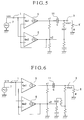
- Fig. 5 is a diagram showing the construction of the amplifier circuit having a feedback circuit for performing the feedback of the video signal after the capacitive coupling to the second input terminal.
- Fig. 6, similarly to Fig. 5, is a diagram showing the construction of the amplifier circuit having a feedback circuit for performing the feedback of the video signal after the capacitive coupling to the second input terminal.
- the feedback circuit shown in Fig. 5 is stable when there is not a terminating resistor, and the feedback circuit shown in Fig. 6 has a good frequency characteristic.
- Fig. 7 is a timing chart showing signal waveforms of the respective portions in the amplifier circuit shown in Fig. 5 or Fig. 6.
- a resistor and a capacitor are connected in series between the terminal of the output side of the capacitive coupling 11 and the second output terminal in Fig. 5, only the capacitor can be also connected.
- a resistor and a capacitor are connected in series between the connecting point of two resistors, connected in series between the terminal of the output side of the capacitive coupling 11 and the ground, and the second output terminal in Fig. 6, only the capacitor can be also connected.
- Fig. 8 is a diagram showing the concrete construction of the amplifier circuit shown in Fig. 1.
- the amplifier circuit has a bandgap circuit 12.
- a bandgap voltage generated in the bandgap circuit 12 is inputted to the base of an NPN transistor (Tr) 13, and an external resistor 14 is connected between the emitter of the NPN transistor 13 and the ground (GND).
- Fig. 9 is a diagram showing the principle of operation of the bandgap circuit 12.
- a bandgap circuit is a circuit for outputting a bandgap voltage (about 1.2 V) for silicon, and has a characteristic that is not fluctuated by temperature.
- a resistor Ra is connected to the emitter of a transistor having N times the size between two transistors having different sizes (1:N), and the same base potential is given to the two transistors so that the same collector currents may flow.
- Vbandgap Vbe+2 ⁇ (Rb/Ra) ⁇ (k ⁇ lnN/q) ⁇ T
- the collector current of the NPN transistor (Tr) 13 shown in Fig. 8 becomes proportional to the absolute temperature. Then, by making currents, mirrored from the collector current of the NPN transistor 13, flow into emitter-coupled differential input circuits 15 and 16, the emitter-coupled differential input circuits 15 and 16 can have conductances (Gm's) of a characteristic not depending on temperature.
- output currents from the emittercoupled differential input circuits 15 and 16 are mirrored by transistors 17 and 18, and are outputted to the second output terminal 4. Furthermore, the currents are mirrored by transistors 19 and 20, and are outputted to the first output terminal 3.
- the output impedance obtained from Fig. 3 small by putting conductances in Gm1>>Gm2, and, at this time, the output impedance becomes Z ⁇ R1(Gm2/Gm1).
- the resistance R1 is several-ten k ⁇
- the current outputted from the first output terminal is several-ten to several-hundred times larger than the current outputted from the second output terminal.
- the amplifier circuit since it is possible to adjust the output level at the time of termination by applying the feedback so that the output impedance may become 75 ⁇ , the amplifier circuit can operate at a supply voltage of 3 V if the signal amplitude of the first output terminal is 1 Vpp.
- the amplifier circuit of the present invention since it is possible to adjust the output level at the time of termination by applying the feedback so that the output impedance may become 75 ⁇ , the amplifier circuit can operate at a supply voltage of 3 V if the signal amplitude of the first output terminal is 1 Vpp, which is different from the output amplitude of 2 Vpp from a conventional video output amplifier circuit. Owing to this, it is possible to provide an amplifier circuit for video output that is operable at a supply voltage of 3 V. In this manner, since it is possible to use a supply voltage of 3 V in a portable apparatus such as a video camera, it is possible to achieve cost reduction by simplification of the construction of a power supply and performance improvement by lengthening continuous duty time of a battery.
- An amplifier circuit for amplifying an input signal and outputting the amplified signal includes a first amplifier for outputting from a first output terminal a current proportional to a difference voltage between voltages at a first input terminal and a second input terminal, and a second amplifier for outputting from a second output terminal a current proportional to a difference voltage between voltages at the first input terminal and the second input terminal and for feeding back a current outputted from the second output terminal to the second input terminal, so that the amplifier circuit is operable at a supply voltage of 3 V.
Abstract
Description
- The present invention relates to an amplifier circuit for outputting an input signal at a specific output impedance, and in particular, to an amplifier circuit that is built in a video camera and the like and is used for amplifying a video signal and the like.
- Conventionally, since an output impedance is specified at 75 ohms in an amplifier circuit for outputting a video signal, the amplifier circuit outputs a signal through a resistor of 75 ohms by driving the signal in a low-impedance output amplifier circuit, the signal being twice as large as a signal at a 75-ohm terminating resistor.
- Nevertheless, it is necessary for the conventional amplifier circuit to output a signal of 2 Vpp in the low-impedance output amplifier circuit so as to output a video signal having an amplitude of 1 Vpp. Therefore, a supply voltage of at least 4 V is required if the low-impedance output amplifier circuit is constructed of a push-pull circuit with bipolar transistors.
- In addition, if the low-impedance output amplifier circuit is constructed in a collector-output type, it is possible to lower the supply voltage to a degree. Nevertheless, it is difficult to operate the low-impedance output amplifier circuit at the supply voltage of 3 V.
- Recently, supply voltages have been reduced so as to get longer battery lives in portable apparatuses, and operation on 3-volt power supplies is also requested in video cameras. Nevertheless, it is not possible for the conventional art to correspond to the requirement.
- An object of the present invention is to provide an amplifier circuit which is operable at a supply voltage of 3 V.
- To attain the above objects, in accordance with an aspect of the present invention, there is provided an amplifier circuit for amplifying an input signal and outputting the amplified signal, which comprises a first amplifier for outputting from a first output terminal a current proportional to a difference voltage between voltages at a first input terminal and a second input terminal, and a second amplifier for outputting from a second output terminal a current proportional to a difference voltage between voltages at the first input terminal and the second input terminal and for feeding back a current outputted from the second output terminal to the second input terminal.
- The above and further objects and features of the present invention will become apparent from the following detailed description of a preferred embodiment thereof taken in conjunction with the accompanying drawings.
-
- Fig. 1 is a diagram showing the fundamental construction of an amplifier circuit according to an embodiment of the present invention.
- Fig. 2 is a diagram showing a state of a signal source being connected to an input terminal of the amplifier circuit shown in Fig. 1 so as to adjust (set) an input-output gain.
- Fig. 3 is a diagram showing a state of a signal source being connected to an output terminal of the amplifier circuit shown in Fig. 1 so as to adjust (set) an output impedance.
- Fig. 4 is a diagram showing the construction at the time of further outputting a signal through capacitive coupling in the amplifier circuit shown in Fig. 1.
- Fig. 5 is a diagram showing the construction at the time of a feedback circuit further being provided for performing feedback of a signal outputted through the capacitive coupling to a second input terminal in the amplifier circuit shown in Fig. 1.
- Fig. 6 is a diagram showing another construction at the time of a feedback circuit further being provided for performing feedback of a signal outputted through the capacitive coupling to a second input terminal in the amplifier circuit shown in Fig. 1.
- Fig. 7 is a timing chart showing waveforms of respective portions in the amplifier circuit shown in Fig. 5 or 6.
- Fig. 8 is a diagram showing the concrete construction of the amplifier circuit shown in Fig. 1.
- Fig. 9 is a diagram for explaining the principle of operation of a bandgap circuit in the amplifier circuit shown in Fig. 8.
-
- Hereinafter, a preferred embodiment of the present invention will be described in detail with reference to the drawings.
- Fig. 1 is a diagram showing the fundamental construction of an amplifier circuit according to the embodiment. In Fig. 1,
reference numeral 1 denotes a first input terminal,reference numeral 2 denotes an second input terminal,reference numeral 3 denotes a first output terminal,reference numeral 4 denotes a second output terminal,reference numeral 5 denotes a first Gm amplifier for outputting a current to thefirst output terminal 3, andreference numeral 6 denotes a second Gm amplifier for outputting a current to thesecond output terminal 4. - Fig. 2 is a diagram showing the construction of the amplifier circuit whose input terminal a signal source is connected to when the input-output gain is determined. In Fig. 2,
reference numeral 7 denotes an input signal source,reference numeral 8 denotes a terminating resistor, andreference numerals first Gm amplifier 5 and thesecond Gm amplifier 6 be Gm1 and Gm2, respectively, and resistances of the terminatingresistor 8 and thefeedback resistors first output terminal 3 and thesecond output terminal 4 be v1 and v2, respectively, the following formulas (1) and (2) can be obtained according to the Kirchhoff's first law at thefirst output terminal 3 and the second output terminal 4: - By expressing the voltage v1 with the input signal vin from the formulas (1) and (2), the following formula (3) can be obtained:
- By means of this construction, the input-output gain is determined by deciding the respective values of the resistances R, R1, and R2 and the conductances Gm1 and Gm2.
- Fig. 3 is a diagram showing the construction of the amplifier circuit whose output terminal a signal source is connected to when an output impedance is determined. When the output impedance is calculated, the following formulas (4) and (5) are obtained according to the Kirchhoff's first law at the
first output terminal 3 and thesecond output terminal 4, similarly to the above: - By expressing the voltage v1 with the input signal vin from the formulas (4) and (5), the following formula (6) can be obtained:
- Here, letting an output impedance at the time of viewing the circuit side from the
first output terminal 3 be Z, the formula (6) can be expressed as the following formula (7), and further the output impedance Z is expressed by the following formula (8): - As described above, by using accurate external resistors as the resistances R1, R2 and R and improving the accuracy of the conductances Gm1 and Gm2, it becomes possible to realize the amplifier circuit having a constant output impedance and a constant input-output gain at the time of the terminating resistor being resistance R.
- Therefore, by adjusting an output level at the time of termination while performing the feedback so that the output impedance becomes 75 Ω, it becomes possible to construct the amplifier circuit which is operable at a supply voltage of 3 V.
- Next, sag correction in an amplifier circuit will be described. Since a video signal is outputted in alternating current and is terminated in the receiving side, the video signal is usually outputted through capacitive coupling (a capacitor). Fig. 4 is a diagram showing the structure of an amplifier circuit for outputting a signal through the capacitive coupling.
- Since a frequency characteristic decreases in the lower frequency domain of a video signal due to a time constant of RC in case of termination through the
capacitive coupling 11, a sag arises in the video signal, resulting in uneven luminance on a picture. - In order to prevent this, it is necessary to correct the reduction of the frequency characteristic at the output terminal by performing feedback of the video signal after the capacitive coupling to the second input terminal.
- Fig. 5 is a diagram showing the construction of the amplifier circuit having a feedback circuit for performing the feedback of the video signal after the capacitive coupling to the second input terminal. Fig. 6, similarly to Fig. 5, is a diagram showing the construction of the amplifier circuit having a feedback circuit for performing the feedback of the video signal after the capacitive coupling to the second input terminal. The feedback circuit shown in Fig. 5 is stable when there is not a terminating resistor, and the feedback circuit shown in Fig. 6 has a good frequency characteristic. Fig. 7 is a timing chart showing signal waveforms of the respective portions in the amplifier circuit shown in Fig. 5 or Fig. 6.
- Incidentally, although a resistor and a capacitor are connected in series between the terminal of the output side of the
capacitive coupling 11 and the second output terminal in Fig. 5, only the capacitor can be also connected. Although a resistor and a capacitor are connected in series between the connecting point of two resistors, connected in series between the terminal of the output side of thecapacitive coupling 11 and the ground, and the second output terminal in Fig. 6, only the capacitor can be also connected. - Fig. 8 is a diagram showing the concrete construction of the amplifier circuit shown in Fig. 1. The amplifier circuit has a
bandgap circuit 12. A bandgap voltage generated in thebandgap circuit 12 is inputted to the base of an NPN transistor (Tr) 13, and anexternal resistor 14 is connected between the emitter of theNPN transistor 13 and the ground (GND). - Here, the details of the
bandgap circuit 12 will be described. Fig. 9 is a diagram showing the principle of operation of thebandgap circuit 12. A bandgap circuit is a circuit for outputting a bandgap voltage (about 1.2 V) for silicon, and has a characteristic that is not fluctuated by temperature. Concretely, a resistor Ra is connected to the emitter of a transistor having N times the size between two transistors having different sizes (1:N), and the same base potential is given to the two transistors so that the same collector currents may flow. The value of the collector current i flowing at this time is shown in the following formula (9), where T represents absolute temperature, k represents the Boltzman's constant, and q represents an electric charge. - Here, by making the collector current i flow through a resistor Rb and adding a voltage between both ends of the resistor Rb to a base-emitter voltage Vbe, a voltage Vbandgap that is not fluctuated by temperature can be obtained as shown in the following formula (10):
Vbe+ 2·(Rb/Ra)·(k·lnN/q)·T - According to the formula (10), it can be seen that a voltage obtained by subtracting the base-emitter voltage Vbe from the bandgap voltage Vbandgap is proportional to the absolute temperature T. By performing current transformation of this voltage with the resistance R, the obtained current is proportional to the absolute temperature T.
- In addition, conductance gm at the time of making a current I flow into a differential input circuit is shown in the following formula (11):
- Therefore, by making a current proportional to the absolute temperature T flow into the differential input circuit, it becomes possible to generate the conductance gm not depending on temperature.
- In this manner, the collector current of the NPN transistor (Tr) 13 shown in Fig. 8 becomes proportional to the absolute temperature. Then, by making currents, mirrored from the collector current of the
NPN transistor 13, flow into emitter-coupleddifferential input circuits differential input circuits - Moreover, output currents from the emittercoupled
differential input circuits transistors 17 and 18, and are outputted to thesecond output terminal 4. Furthermore, the currents are mirrored bytransistors first output terminal 3. - In an amplifier circuit capable of correcting the sag, the less the capacitor in the feedback circuit is, the better it is from the viewpoint of part cost and size, so that the larger the resistor used in the feedback circuit is, the better it is. On the other hand, it becomes possible to make the output impedance obtained from Fig. 3 small by putting conductances in Gm1>>Gm2, and, at this time, the output impedance becomes Z ≒ R1(Gm2/Gm1).
- For example, in a case where the resistance R1 is several-ten kΩ, it is good to set the ratio of the conductances Gm1 and Gm2 at about 100 so that the output impedance Z may become 75 Ω. On the other hand, in consideration of mirror accuracy and consumption current, it is adequate to set the ratio of the conductances Gm1 and Gm2 at from several-ten to several-hundred. In this case, the current outputted from the first output terminal is several-ten to several-hundred times larger than the current outputted from the second output terminal.
- In this manner, in the amplifier circuit according to the embodiment, since it is possible to adjust the output level at the time of termination by applying the feedback so that the output impedance may become 75 Ω, the amplifier circuit can operate at a supply voltage of 3 V if the signal amplitude of the first output terminal is 1 Vpp.
- According to the amplifier circuit of the present invention, since it is possible to adjust the output level at the time of termination by applying the feedback so that the output impedance may become 75 Ω, the amplifier circuit can operate at a supply voltage of 3 V if the signal amplitude of the first output terminal is 1 Vpp, which is different from the output amplitude of 2 Vpp from a conventional video output amplifier circuit. Owing to this, it is possible to provide an amplifier circuit for video output that is operable at a supply voltage of 3 V. In this manner, since it is possible to use a supply voltage of 3 V in a portable apparatus such as a video camera, it is possible to achieve cost reduction by simplification of the construction of a power supply and performance improvement by lengthening continuous duty time of a battery.
- In addition, it is possible to provide an amplifier circuit having excellent temperature stability since it is possible to construct the amplifier circuit so that its conductances do not change with temperature.
- Furthermore, it is possible to make an output impedance and an input-output gain constant.
- Moreover, it is possible to prevent a sag from arising in a video signal and to make stability good at the time of a terminating resistor not being there since it is possible to correct the reduction of a frequency characteristic.
- An amplifier circuit for amplifying an input signal and outputting the amplified signal includes a first amplifier for outputting from a first output terminal a current proportional to a difference voltage between voltages at a first input terminal and a second input terminal, and a second amplifier for outputting from a second output terminal a current proportional to a difference voltage between voltages at the first input terminal and the second input terminal and for feeding back a current outputted from the second output terminal to the second input terminal, so that the amplifier circuit is operable at a supply voltage of 3 V.
Claims (6)
- An amplifier circuit for amplifying an input signal and outputting the amplified signal, said amplifier circuit comprising:(A) a first amplifier for outputting from a first output terminal a current proportional to a difference voltage between voltages at a first input terminal and a second input terminal; and(B) a second amplifier for outputting from a second output terminal a current proportional to a difference voltage between voltages at the first input terminal and the second input terminal and for feeding back a current outputted from the second output terminal to the second input terminal.
- An amplifier circuit according to claim 1, wherein the current outputted from the first output terminal is made several-ten times to several-hundred times larger than the current outputted from the second output terminal.
- An amplifier circuit according to claim 1, further comprising a first resistor connected between the first output terminal and the second output terminal, and a second resistor connected between the second output terminal and a ground, and wherein an input signal is inputted to the first input terminal and an output signal is outputted from the first output terminal.
- An amplifier circuit according to claim 1, further comprising a first resistor connected between the first output terminal and the second output terminal, a second resistor connected between the second output terminal and a ground, a first capacitor element one terminal of which is connected to the first output terminal, a second capacitor element, or the second capacitor element and a third resistor in series, connected between the other terminal of said first capacitor element and the second output terminal, and a third capacitor element and a fourth resistor in series connected between the second output terminal and the ground, and wherein an input signal is inputted to the first input terminal and an output signal is outputted from the other terminal of said first capacitor element.
- An amplifier circuit according to claim 1, further comprising a first resistor connected between the first output terminal and the second output terminal, a second resistor connected between the second output terminal and a ground, a first capacitor element one terminal of which is connected to the first output terminal, a third resistor connected between the other terminal of said first capacitor element and the ground, a second capacitor element, or the second capacitor element and a fourth resistor in series, connected between the other terminal of said first capacitor element and the second output terminal, and a third capacitor element and a fifth resistor in series connected between the second output terminal and the ground, and wherein an input signal is inputted to the first input terminal and an output signal is outputted from the other terminal of said first capacitor element.
- An amplifier circuit according to claim 1, further comprising a bandgap circuit for generating a bandgap voltage, a current generating circuit for generating a current proportional to absolute temperature, said current generating circuit being composed of an NPN transistor element, a base terminal of which the bandgap voltage generated by said bandgap circuit is supplied to, and a resistor connected between an emitter terminal of said NPN transistor element and a ground, and a differential input circuit which operates by receiving a current proportional to the current generated by said current generating circuit as a drive current and which is connected to the first output terminal and the second output terminal.
Applications Claiming Priority (3)
| Application Number | Priority Date | Filing Date | Title |
|---|---|---|---|
| JP27033797 | 1997-09-18 | ||
| JP270337/97 | 1997-09-18 | ||
| JP9270337A JPH1197954A (en) | 1997-09-18 | 1997-09-18 | Amplifying circuit |
Publications (2)
| Publication Number | Publication Date |
|---|---|
| EP0903847A1 true EP0903847A1 (en) | 1999-03-24 |
| EP0903847B1 EP0903847B1 (en) | 2004-03-17 |
Family
ID=17484856
Family Applications (1)
| Application Number | Title | Priority Date | Filing Date |
|---|---|---|---|
| EP98117672A Expired - Lifetime EP0903847B1 (en) | 1997-09-18 | 1998-09-17 | Amplifier circuit |
Country Status (4)
| Country | Link |
|---|---|
| US (1) | US6091294A (en) |
| EP (1) | EP0903847B1 (en) |
| JP (1) | JPH1197954A (en) |
| DE (1) | DE69822389T2 (en) |
Families Citing this family (5)
| Publication number | Priority date | Publication date | Assignee | Title |
|---|---|---|---|---|
| US6466089B2 (en) * | 2000-10-11 | 2002-10-15 | Texas Instruments Incorporated | Control circuit for increasing the output inpedance of a transconductor |
| JP4407881B2 (en) | 2002-10-16 | 2010-02-03 | ローム株式会社 | Buffer circuit and driver IC |
| US6937099B2 (en) * | 2003-12-04 | 2005-08-30 | Analog Devices, Inc. | Op-amp configurable in a non-inverting mode with a closed loop gain greater than one with output voltage correction for a time varying voltage reference of the op-amp, and a method for correcting the output voltage of such an op-amp for a time varying voltage reference |
| KR100921515B1 (en) | 2006-12-05 | 2009-10-15 | 한국전자통신연구원 | Simplified Nauta Operational Transconductance Amplifier |
| JP2008181812A (en) | 2007-01-25 | 2008-08-07 | Toyota Motor Corp | Fuel cell manufacturing device and fuel cell |
Citations (1)
| Publication number | Priority date | Publication date | Assignee | Title |
|---|---|---|---|---|
| US4929909A (en) * | 1989-03-27 | 1990-05-29 | Analog Devices, Inc. | Differential amplifier with gain compensation |
Family Cites Families (3)
| Publication number | Priority date | Publication date | Assignee | Title |
|---|---|---|---|---|
| GB1204617A (en) * | 1968-04-10 | 1970-09-09 | Cossor Ltd A C | Circuit providing a floating output |
| US5027081A (en) * | 1990-05-03 | 1991-06-25 | Motorola, Inc. | High gain differential-to-single ended amplifier having a tee network feedback loop |
| TW239239B (en) * | 1993-07-14 | 1995-01-21 | Philips Electronics Nv |
-
1997
- 1997-09-18 JP JP9270337A patent/JPH1197954A/en active Pending
-
1998
- 1998-09-10 US US09/150,564 patent/US6091294A/en not_active Expired - Lifetime
- 1998-09-17 EP EP98117672A patent/EP0903847B1/en not_active Expired - Lifetime
- 1998-09-17 DE DE69822389T patent/DE69822389T2/en not_active Expired - Lifetime
Patent Citations (1)
| Publication number | Priority date | Publication date | Assignee | Title |
|---|---|---|---|---|
| US4929909A (en) * | 1989-03-27 | 1990-05-29 | Analog Devices, Inc. | Differential amplifier with gain compensation |
Non-Patent Citations (3)
| Title |
|---|
| A.M. SOLIMAN: "Design of High-Frequency Amplifiers", IEEE CIRCUITS AND SYSTEMS MAGAZINE., vol. 5, no. 2, June 1983 (1983-06-01), NEW YORK US, pages 9 - 11, XP002087773 * |
| GRAEME J: "OP-AMP DISTORTION MEASUREMENT BYPASSES TEST-EQUIPMENT LIMITS DESIGNER'S GUIDE TO MEASURING OP-AMP DISTORTION PART 1", EDN ELECTRICAL DESIGN NEWS, vol. 37, no. 4, 17 February 1992 (1992-02-17), pages 133 - 136, XP000292859 * |
| HAIDEH KHORRAMABADI ET AL: "A HIGHLY EFFICIENT CMOS LINE DRIVER WITH 80-DB LINEARITY FOR ISDN U-INTERFACE APPLICATIONS", IEEE JOURNAL OF SOLID-STATE CIRCUITS, vol. 27, no. 12, 1 December 1992 (1992-12-01), pages 1723 - 1729, XP000329021 * |
Also Published As
| Publication number | Publication date |
|---|---|
| JPH1197954A (en) | 1999-04-09 |
| DE69822389D1 (en) | 2004-04-22 |
| DE69822389T2 (en) | 2005-03-10 |
| US6091294A (en) | 2000-07-18 |
| EP0903847B1 (en) | 2004-03-17 |
Similar Documents
| Publication | Publication Date | Title |
|---|---|---|
| US6642741B2 (en) | Electronically adjustable integrated circuit input/output termination method and apparatus | |
| EP0439071B1 (en) | Logarithmic amplifier | |
| US6091294A (en) | Amplifier circuit | |
| EP0314218B1 (en) | Amplifier arrangement and display device including said amplifier arrangement | |
| JPH0537822A (en) | Gamma correction circuit | |
| US4725790A (en) | Broadband DC level shift circuit with feedback | |
| US6313884B1 (en) | Gamma correction | |
| US6570427B2 (en) | Variable transconductance amplifier | |
| KR100375386B1 (en) | Wafer stage temperature compensation of integrated circuits | |
| JPH0918745A (en) | Video signal clamping circuit | |
| EP1676362B1 (en) | Electronic circuit for amplification of a bipolar signal | |
| JP3107590B2 (en) | Current polarity conversion circuit | |
| JPH0527282B2 (en) | ||
| JP3534275B2 (en) | Current source and integrated circuit | |
| JP3600187B2 (en) | Emitter follower circuit | |
| JP3509167B2 (en) | Current mirror device | |
| JP3216753B2 (en) | DA conversion circuit device | |
| JP2793194B2 (en) | Constant current circuit | |
| JP3165173B2 (en) | Capacitance sensor circuit | |
| JP3146088B2 (en) | Variable reactance circuit | |
| JPH0716138B2 (en) | Amplifier circuit device | |
| JP2853485B2 (en) | Voltage-current converter | |
| JP2722769B2 (en) | Gain control circuit | |
| JP2680748B2 (en) | Coupling capacitance circuit | |
| JPH0122288Y2 (en) |
Legal Events
| Date | Code | Title | Description |
|---|---|---|---|
| PUAI | Public reference made under article 153(3) epc to a published international application that has entered the european phase |
Free format text: ORIGINAL CODE: 0009012 |
|
| AK | Designated contracting states |
Kind code of ref document: A1 Designated state(s): DE FR GB NL |
|
| AX | Request for extension of the european patent |
Free format text: AL;LT;LV;MK;RO;SI |
|
| 17P | Request for examination filed |
Effective date: 19990811 |
|
| AKX | Designation fees paid |
Free format text: DE FR GB NL |
|
| 17Q | First examination report despatched |
Effective date: 20020819 |
|
| GRAP | Despatch of communication of intention to grant a patent |
Free format text: ORIGINAL CODE: EPIDOSNIGR1 |
|
| GRAS | Grant fee paid |
Free format text: ORIGINAL CODE: EPIDOSNIGR3 |
|
| GRAA | (expected) grant |
Free format text: ORIGINAL CODE: 0009210 |
|
| AK | Designated contracting states |
Kind code of ref document: B1 Designated state(s): DE FR GB NL |
|
| REG | Reference to a national code |
Ref country code: GB Ref legal event code: FG4D |
|
| REF | Corresponds to: |
Ref document number: 69822389 Country of ref document: DE Date of ref document: 20040422 Kind code of ref document: P |
|
| ET | Fr: translation filed | ||
| PLBE | No opposition filed within time limit |
Free format text: ORIGINAL CODE: 0009261 |
|
| STAA | Information on the status of an ep patent application or granted ep patent |
Free format text: STATUS: NO OPPOSITION FILED WITHIN TIME LIMIT |
|
| 26N | No opposition filed |
Effective date: 20041220 |
|
| PGFP | Annual fee paid to national office [announced via postgrant information from national office to epo] |
Ref country code: FR Payment date: 20111005 Year of fee payment: 14 |
|
| PGFP | Annual fee paid to national office [announced via postgrant information from national office to epo] |
Ref country code: NL Payment date: 20110923 Year of fee payment: 14 |
|
| REG | Reference to a national code |
Ref country code: NL Ref legal event code: V1 Effective date: 20130401 |
|
| REG | Reference to a national code |
Ref country code: FR Ref legal event code: ST Effective date: 20130531 |
|
| PG25 | Lapsed in a contracting state [announced via postgrant information from national office to epo] |
Ref country code: NL Free format text: LAPSE BECAUSE OF NON-PAYMENT OF DUE FEES Effective date: 20130401 Ref country code: FR Free format text: LAPSE BECAUSE OF NON-PAYMENT OF DUE FEES Effective date: 20121001 |
|
| PGFP | Annual fee paid to national office [announced via postgrant information from national office to epo] |
Ref country code: GB Payment date: 20150922 Year of fee payment: 18 Ref country code: DE Payment date: 20150930 Year of fee payment: 18 |
|
| REG | Reference to a national code |
Ref country code: DE Ref legal event code: R119 Ref document number: 69822389 Country of ref document: DE |
|
| GBPC | Gb: european patent ceased through non-payment of renewal fee |
Effective date: 20160917 |
|
| PG25 | Lapsed in a contracting state [announced via postgrant information from national office to epo] |
Ref country code: DE Free format text: LAPSE BECAUSE OF NON-PAYMENT OF DUE FEES Effective date: 20170401 Ref country code: GB Free format text: LAPSE BECAUSE OF NON-PAYMENT OF DUE FEES Effective date: 20160917 |