EP0903791A2 - Bauteil zur optischen Datenübertragung - Google Patents
Bauteil zur optischen Datenübertragung Download PDFInfo
- Publication number
- EP0903791A2 EP0903791A2 EP98110243A EP98110243A EP0903791A2 EP 0903791 A2 EP0903791 A2 EP 0903791A2 EP 98110243 A EP98110243 A EP 98110243A EP 98110243 A EP98110243 A EP 98110243A EP 0903791 A2 EP0903791 A2 EP 0903791A2
- Authority
- EP
- European Patent Office
- Prior art keywords
- chip
- integrated circuit
- component according
- emitter
- detector chip
- Prior art date
- Legal status (The legal status is an assumption and is not a legal conclusion. Google has not performed a legal analysis and makes no representation as to the accuracy of the status listed.)
- Granted
Links
Images
Classifications
-
- G—PHYSICS
- G02—OPTICS
- G02B—OPTICAL ELEMENTS, SYSTEMS OR APPARATUS
- G02B6/00—Light guides; Structural details of arrangements comprising light guides and other optical elements, e.g. couplings
- G02B6/24—Coupling light guides
- G02B6/42—Coupling light guides with opto-electronic elements
- G02B6/4201—Packages, e.g. shape, construction, internal or external details
- G02B6/4246—Bidirectionally operating package structures
-
- H—ELECTRICITY
- H10—SEMICONDUCTOR DEVICES; ELECTRIC SOLID-STATE DEVICES NOT OTHERWISE PROVIDED FOR
- H10F—INORGANIC SEMICONDUCTOR DEVICES SENSITIVE TO INFRARED RADIATION, LIGHT, ELECTROMAGNETIC RADIATION OF SHORTER WAVELENGTH OR CORPUSCULAR RADIATION
- H10F55/00—Radiation-sensitive semiconductor devices covered by groups H10F10/00, H10F19/00 or H10F30/00 being structurally associated with electric light sources and electrically or optically coupled thereto
- H10F55/20—Radiation-sensitive semiconductor devices covered by groups H10F10/00, H10F19/00 or H10F30/00 being structurally associated with electric light sources and electrically or optically coupled thereto wherein the electric light source controls the radiation-sensitive semiconductor devices, e.g. optocouplers
- H10F55/25—Radiation-sensitive semiconductor devices covered by groups H10F10/00, H10F19/00 or H10F30/00 being structurally associated with electric light sources and electrically or optically coupled thereto wherein the electric light source controls the radiation-sensitive semiconductor devices, e.g. optocouplers wherein the radiation-sensitive devices and the electric light source are all semiconductor devices
-
- H—ELECTRICITY
- H10—SEMICONDUCTOR DEVICES; ELECTRIC SOLID-STATE DEVICES NOT OTHERWISE PROVIDED FOR
- H10F—INORGANIC SEMICONDUCTOR DEVICES SENSITIVE TO INFRARED RADIATION, LIGHT, ELECTROMAGNETIC RADIATION OF SHORTER WAVELENGTH OR CORPUSCULAR RADIATION
- H10F77/00—Constructional details of devices covered by this subclass
- H10F77/40—Optical elements or arrangements
-
- H—ELECTRICITY
- H10—SEMICONDUCTOR DEVICES; ELECTRIC SOLID-STATE DEVICES NOT OTHERWISE PROVIDED FOR
- H10W—GENERIC PACKAGES, INTERCONNECTIONS, CONNECTORS OR OTHER CONSTRUCTIONAL DETAILS OF DEVICES COVERED BY CLASS H10
- H10W74/00—Encapsulations, e.g. protective coatings
- H10W74/10—Encapsulations, e.g. protective coatings characterised by their shape or disposition
-
- H—ELECTRICITY
- H10—SEMICONDUCTOR DEVICES; ELECTRIC SOLID-STATE DEVICES NOT OTHERWISE PROVIDED FOR
- H10W—GENERIC PACKAGES, INTERCONNECTIONS, CONNECTORS OR OTHER CONSTRUCTIONAL DETAILS OF DEVICES COVERED BY CLASS H10
- H10W90/00—Package configurations
- H10W90/701—Package configurations characterised by the relative positions of pads or connectors relative to package parts
- H10W90/751—Package configurations characterised by the relative positions of pads or connectors relative to package parts of bond wires
- H10W90/756—Package configurations characterised by the relative positions of pads or connectors relative to package parts of bond wires between a chip and a stacked lead frame, conducting package substrate or heat sink
Definitions
- a component for directed, bi-directional optical communication wherein in a single- or multi-part housing as components, an emitter chip for transmitting IR beams, a detector chip for receiving IR beams, an integrated circuit for amplifying the transmission - And receiving power and an optical system with an optical axis for bundling the emitted and received beams are arranged. It is characteristic that the detector chip and the emitter chip are arranged concentrically to one another on the optical axis of the optical system and on the integrated circuit.
Landscapes
- Physics & Mathematics (AREA)
- General Physics & Mathematics (AREA)
- Optics & Photonics (AREA)
- Optical Communication System (AREA)
- Light Receiving Elements (AREA)
- Led Device Packages (AREA)
Abstract
Description
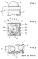
- Fig. 1:
- ein erfindungsgemäßer Transceiver in Seitenansicht,
- Fig. 2:
- der Transceiver nach Fig. 1a in aufgeschnittener Darstellung,
- Fig. 3:
- ein Transceiver nach dem Stand der Technik in perspektivischer Darstellung.
Claims (10)
- Bauteil zur gerichteten, bidirektionalen optischen Datenübertragung, bei dem in einem ein- oder mehrteiligen Gehäuse (3) als Bauteile ein Emitterchip (10) zum Aussenden von IR-Strahlen, ein Detektorchip (8) zum Empfangen von IR-Strahlen, ein integrierter Schaltkreis (6) zum verstärken der Sende- und Empfangsleistung und ein optisches System (2) mit einer optischen Achse zur Bündelung der ausgesendeten und empfangenen Strahlen angeordnet sind, dadurch gekennzeichnet, daß das Detektorchip (8) und der Emitterchip (10) konzentrisch zur optischen Achse des optischen Systems (2) aufeinander und auf dem integrierten Schaltkreis (6) angeordnet sind.
- Bauteil nach Anspruch 1, dadurch gekennzeichnet, daß das Emitterchip (10) als oberstes Bauteil angeordnet ist.
- Bauteil nach Anspruch 1 oder 2, dadurch gekennzeichnet, daß die Fläche des integrierten Schaltkreises (6) größer als die Fläche des Detektorchips (8) und die Fläche des Detektorchips (8) größer als die Fläche des Emitterchips (10) ist.
- Bauteil nach Anspruch 1, 2 oder 3, dadurch gekennzeichnet, daß die Oberfläche des Detektorchips (8) in ihrem Zentrum eine Metallisierung (11a, 11b) aufweist, die als Montagefläche (11b) für das Emitterchip (10) dient.
- Bauteil nach Anspruch 4, dadurch gekennzeichnet, daß die Metallisierung (11b) auf dem Detektorchip (8) als Anschlußpad für einen Bonddraht (12) dient.
- Bauteil nach Anspruch 4, dadurch gekennzeichnet, daß der Emitterchip (10) eine Rückseitenmetallisierung aufweist, die mittels Lot oder leitfähigem Kleber in Kontakt mit der Montagefläche (11b) steht.
- Bauteil nach einem der vorangehenden Ansprüche, dadurch gekennzeichnet, daß Bonddrähte (12) zwischen den Anschlußpads (7) des integrierten Schaltkreises (6) und den Anschlußpads (9) des Detektorchips (8), zwischen den Anschlußpads (7) des integrierten Schaltkreises (6) und der Metallisierung (11b) auf dem Detektorchip (8), zwischen den Anschlußpads (7) des integrierten Schaltkreises (6) und den Anschlußbeinchen (4) und/oder zwischen dem Anschlußpad (11a) des Emitterchips (10) und den Anschlußbeinchen (4) angeordnet sind.
- Bauteil nach einem der vorangehenden Ansprüche, dadurch gekennzeichnet, daß die Bauteile (6, 8, 10) auf einem Träger (5) montiert sind.
- Bauteil nach Anspruch 8, dadurch gekennzeichnet, daß es sich bei dem Träger (5) um einen metallischen Streifenträger handelt.
- Bauteil nach einem der vorangehenden Ansprüche, dadurch gekennzeichnet, daß das Gehäuse (3) aus einer thermo- oder duroplastischen und für IR-Strahlen transparenten Vergußmasse besteht.
Applications Claiming Priority (2)
| Application Number | Priority Date | Filing Date | Title |
|---|---|---|---|
| DE19727632 | 1997-06-28 | ||
| DE19727632A DE19727632C2 (de) | 1997-06-28 | 1997-06-28 | Sende-/Empfangsgerät zur optischen Datenübertragung |
Publications (3)
| Publication Number | Publication Date |
|---|---|
| EP0903791A2 true EP0903791A2 (de) | 1999-03-24 |
| EP0903791A3 EP0903791A3 (de) | 1999-12-22 |
| EP0903791B1 EP0903791B1 (de) | 2001-11-21 |
Family
ID=7834004
Family Applications (1)
| Application Number | Title | Priority Date | Filing Date |
|---|---|---|---|
| EP98110243A Expired - Lifetime EP0903791B1 (de) | 1997-06-28 | 1998-06-05 | Bauteil zur optischen Datenübertragung |
Country Status (6)
| Country | Link |
|---|---|
| US (1) | US6320686B1 (de) |
| EP (1) | EP0903791B1 (de) |
| JP (1) | JPH1197748A (de) |
| DE (2) | DE19727632C2 (de) |
| ES (1) | ES2166119T3 (de) |
| PL (1) | PL193016B1 (de) |
Families Citing this family (14)
| Publication number | Priority date | Publication date | Assignee | Title |
|---|---|---|---|---|
| DE19823213C2 (de) | 1998-05-25 | 2002-02-21 | Infineon Technologies Ag | Bidirektionale optische Sende- und Empfangseinrichtung |
| DE19834090A1 (de) | 1998-07-29 | 2000-02-03 | Heidenhain Gmbh Dr Johannes | Optoelektronische Sende- und Empfangseinheit |
| US6721503B1 (en) * | 1998-08-26 | 2004-04-13 | Georgia Tech Research Corporation | System and method for bi-directional optical communication using stacked emitters and detectors |
| DE10043127A1 (de) * | 1999-08-31 | 2001-08-30 | Rohm Co Ltd | Infrarot-Daten-Kommunikationsmodul und Verfahren zu dessen Herstellung |
| JP3930710B2 (ja) * | 2000-09-13 | 2007-06-13 | シチズン電子株式会社 | チップ型発光ダイオード及びその製造方法 |
| DE10058622A1 (de) * | 2000-11-15 | 2002-05-29 | Vishay Semiconductor Gmbh | Gemouldetes elektronisches Bauelement |
| DE10058608A1 (de) | 2000-11-25 | 2002-05-29 | Vishay Semiconductor Gmbh | Leiterstreifenanordnung für ein gemouldetes elektronisches Bauelement und Verfahren zum Moulden |
| US6731415B1 (en) | 2002-03-28 | 2004-05-04 | Terabeam Corporation | Multi-aperture holographic optical element for use in a free space optical communication system |
| US6661546B1 (en) | 2002-03-28 | 2003-12-09 | Terabeam Corporation | Multi-aperture holographic optical element for illumination sensing in a free space optical communication system |
| US7978800B2 (en) | 2002-10-10 | 2011-07-12 | Finisar Corporation | Circuit for converting a transponder controller chip output into an appropriate input signal for a host device |
| US7023563B2 (en) * | 2003-02-14 | 2006-04-04 | Chian Chiu Li | Interferometric optical imaging and storage devices |
| US7397022B2 (en) * | 2004-04-01 | 2008-07-08 | Vishay Semiconductor Gmbh | Sensor arrangement to prevent reference light incident on side of photodiode |
| JP4210240B2 (ja) * | 2004-06-03 | 2009-01-14 | ローム株式会社 | 光通信モジュール |
| US7385175B2 (en) * | 2004-09-18 | 2008-06-10 | Chian Chiu Li | Bi-directional optical transmission system and method |
Family Cites Families (7)
| Publication number | Priority date | Publication date | Assignee | Title |
|---|---|---|---|---|
| DE2629356C2 (de) * | 1976-06-30 | 1983-07-21 | AEG-Telefunken Nachrichtentechnik GmbH, 7150 Backnang | Elektrooptischer Wandler zum Senden oder Empfangen |
| GB2011610A (en) * | 1977-12-23 | 1979-07-11 | Elliot Bros Ltd | Fibre optic terminal |
| DE3502634A1 (de) * | 1985-01-26 | 1985-06-20 | Deutsche Forschungs- und Versuchsanstalt für Luft- und Raumfahrt e.V., 5000 Köln | Optisch-elektronischer entfernungsmesser |
| JPH04237005A (ja) * | 1991-01-22 | 1992-08-25 | Fujitsu Ltd | 受光モジュール |
| US5140152A (en) * | 1991-05-31 | 1992-08-18 | The University Of Colorado Foundation, Inc. | Full duplex optoelectronic device with integral emitter/detector pair |
| US5267070A (en) * | 1992-05-05 | 1993-11-30 | The United States Of America As Represented By The Secretary Of The Navy | Underwater IR communication system |
| US5506445A (en) * | 1994-06-24 | 1996-04-09 | Hewlett-Packard Company | Optical transceiver module |
-
1997
- 1997-06-28 DE DE19727632A patent/DE19727632C2/de not_active Expired - Lifetime
-
1998
- 1998-06-04 JP JP10192238A patent/JPH1197748A/ja active Pending
- 1998-06-05 ES ES98110243T patent/ES2166119T3/es not_active Expired - Lifetime
- 1998-06-05 EP EP98110243A patent/EP0903791B1/de not_active Expired - Lifetime
- 1998-06-05 DE DE59802691T patent/DE59802691D1/de not_active Expired - Lifetime
- 1998-06-10 PL PL326787A patent/PL193016B1/pl unknown
- 1998-06-25 US US09/104,766 patent/US6320686B1/en not_active Expired - Lifetime
Also Published As
| Publication number | Publication date |
|---|---|
| DE19727632C2 (de) | 1999-10-28 |
| PL193016B1 (pl) | 2007-01-31 |
| JPH1197748A (ja) | 1999-04-09 |
| US6320686B1 (en) | 2001-11-20 |
| DE59802691D1 (de) | 2002-02-21 |
| ES2166119T3 (es) | 2002-04-01 |
| PL326787A1 (en) | 1999-01-04 |
| EP0903791A3 (de) | 1999-12-22 |
| DE19727632A1 (de) | 1999-01-28 |
| EP0903791B1 (de) | 2001-11-21 |
Similar Documents
| Publication | Publication Date | Title |
|---|---|---|
| DE19727633C2 (de) | Bauteil zur gerichteten, bidirektionalen, optischen Datenübertragung | |
| EP0903791B1 (de) | Bauteil zur optischen Datenübertragung | |
| EP0809304B1 (de) | Optoelektronischer Wandler und dessen Herstellungsverfahren | |
| DE69129547T2 (de) | Packung für eine optoelektronische vorrichtung und verfahren zu ihrer herstellung | |
| DE3633251A1 (de) | Optoelektronisches koppelelement | |
| DE69403622T2 (de) | Photoelektrischer Unterbrecher und Verfahren zu seiner Herstellung | |
| DE19536454B4 (de) | Optoelektronisches Halbleiter-Bauelement | |
| DE10128419B4 (de) | Festkörper-Bildaufnahmeeinrichtung mit Mikrolinse und Unterfüllung | |
| EP1199753A2 (de) | Optoelektronisches Halbleiter-Bauelement | |
| DE3633181A1 (de) | Verfahren zur herstellung eines optokopplers bzw. einer reflexlichtschranke und zugehoeriger optokoppler bzw. zugehoerige reflexlichtschranke | |
| DE10217073A1 (de) | Miniatur-Halbleitergehäuse für optoelektronische Bauelemente | |
| EP0645827A2 (de) | Optokoppler und Verfahren zu dessen Herstellung | |
| DE10255625A1 (de) | Optisches Sender- Empfängermodul und das Modul verwendende elektronische Vorrichtung | |
| DE19652030A1 (de) | Infrarotsendeempfänger und Verfahren zum Einkapseln desselben | |
| DE102008021435A1 (de) | Gehäuse für LEDs mit hoher Leistung | |
| EP0712161B1 (de) | Halbleiterbaugruppe für die bidirektionale, leitungsungebundene, optische Datenübertragung | |
| EP1379903A1 (de) | Sendemodul für eine optische signalübertragung | |
| DE102007046769A1 (de) | Sensoranordnung | |
| EP0875770A1 (de) | Opto-electronische Sensoranordnung | |
| EP1717871A2 (de) | Oberflächenmontierbares optoelektronisches Bauelement | |
| DE102010000697A1 (de) | Faseroptisches Transceiver (FOT) Modul und Verfahren zur Herstellung eines FOT Moduls | |
| DE102005046164A1 (de) | Röntgendetektor | |
| JP4486591B2 (ja) | リード端子導出型電子部品 | |
| EP0994509A2 (de) | Bauteil zur optischen Datenübertragung | |
| EP3355075B1 (de) | Sensoranordnung |
Legal Events
| Date | Code | Title | Description |
|---|---|---|---|
| PUAI | Public reference made under article 153(3) epc to a published international application that has entered the european phase |
Free format text: ORIGINAL CODE: 0009012 |
|
| AK | Designated contracting states |
Kind code of ref document: A2 Designated state(s): DE ES FR GB IT |
|
| AX | Request for extension of the european patent |
Free format text: AL;LT;LV;MK;RO;SI |
|
| PUAL | Search report despatched |
Free format text: ORIGINAL CODE: 0009013 |
|
| AK | Designated contracting states |
Kind code of ref document: A3 Designated state(s): AT BE CH CY DE DK ES FI FR GB GR IE IT LI LU MC NL PT SE |
|
| AX | Request for extension of the european patent |
Free format text: AL;LT;LV;MK;RO;SI |
|
| RIC1 | Information provided on ipc code assigned before grant |
Free format text: 6H 01L 31/167 A, 6H 01L 31/147 B, 6H 01L 25/16 B, 6G 02B 6/42 B |
|
| 17P | Request for examination filed |
Effective date: 19991213 |
|
| AKX | Designation fees paid |
Free format text: DE ES FR GB IT |
|
| GRAG | Despatch of communication of intention to grant |
Free format text: ORIGINAL CODE: EPIDOS AGRA |
|
| 17Q | First examination report despatched |
Effective date: 20010320 |
|
| GRAG | Despatch of communication of intention to grant |
Free format text: ORIGINAL CODE: EPIDOS AGRA |
|
| GRAH | Despatch of communication of intention to grant a patent |
Free format text: ORIGINAL CODE: EPIDOS IGRA |
|
| ITF | It: translation for a ep patent filed | ||
| GRAH | Despatch of communication of intention to grant a patent |
Free format text: ORIGINAL CODE: EPIDOS IGRA |
|
| GRAA | (expected) grant |
Free format text: ORIGINAL CODE: 0009210 |
|
| AK | Designated contracting states |
Kind code of ref document: B1 Designated state(s): DE ES FR GB IT |
|
| REG | Reference to a national code |
Ref country code: GB Ref legal event code: IF02 |
|
| GBT | Gb: translation of ep patent filed (gb section 77(6)(a)/1977) |
Effective date: 20020121 |
|
| REF | Corresponds to: |
Ref document number: 59802691 Country of ref document: DE Date of ref document: 20020221 |
|
| REG | Reference to a national code |
Ref country code: ES Ref legal event code: FG2A Ref document number: 2166119 Country of ref document: ES Kind code of ref document: T3 |
|
| ET | Fr: translation filed | ||
| PLBE | No opposition filed within time limit |
Free format text: ORIGINAL CODE: 0009261 |
|
| STAA | Information on the status of an ep patent application or granted ep patent |
Free format text: STATUS: NO OPPOSITION FILED WITHIN TIME LIMIT |
|
| 26N | No opposition filed | ||
| REG | Reference to a national code |
Ref country code: FR Ref legal event code: PLFP Year of fee payment: 19 |
|
| REG | Reference to a national code |
Ref country code: FR Ref legal event code: PLFP Year of fee payment: 20 |
|
| PGFP | Annual fee paid to national office [announced via postgrant information from national office to epo] |
Ref country code: FR Payment date: 20170621 Year of fee payment: 20 Ref country code: GB Payment date: 20170620 Year of fee payment: 20 Ref country code: DE Payment date: 20170621 Year of fee payment: 20 |
|
| PGFP | Annual fee paid to national office [announced via postgrant information from national office to epo] |
Ref country code: IT Payment date: 20170622 Year of fee payment: 20 |
|
| PGFP | Annual fee paid to national office [announced via postgrant information from national office to epo] |
Ref country code: ES Payment date: 20170724 Year of fee payment: 20 |
|
| REG | Reference to a national code |
Ref country code: DE Ref legal event code: R071 Ref document number: 59802691 Country of ref document: DE |
|
| REG | Reference to a national code |
Ref country code: GB Ref legal event code: PE20 Expiry date: 20180604 |
|
| PG25 | Lapsed in a contracting state [announced via postgrant information from national office to epo] |
Ref country code: GB Free format text: LAPSE BECAUSE OF EXPIRATION OF PROTECTION Effective date: 20180604 |
|
| REG | Reference to a national code |
Ref country code: ES Ref legal event code: FD2A Effective date: 20220103 |
|
| PG25 | Lapsed in a contracting state [announced via postgrant information from national office to epo] |
Ref country code: ES Free format text: LAPSE BECAUSE OF EXPIRATION OF PROTECTION Effective date: 20180606 |