EP0903791A2 - Apparatus for optical transmission of data - Google Patents
Apparatus for optical transmission of data Download PDFInfo
- Publication number
- EP0903791A2 EP0903791A2 EP98110243A EP98110243A EP0903791A2 EP 0903791 A2 EP0903791 A2 EP 0903791A2 EP 98110243 A EP98110243 A EP 98110243A EP 98110243 A EP98110243 A EP 98110243A EP 0903791 A2 EP0903791 A2 EP 0903791A2
- Authority
- EP
- European Patent Office
- Prior art keywords
- chip
- integrated circuit
- component according
- emitter
- detector chip
- Prior art date
- Legal status (The legal status is an assumption and is not a legal conclusion. Google has not performed a legal analysis and makes no representation as to the accuracy of the status listed.)
- Granted
Links
Images
Classifications
-
- G—PHYSICS
- G02—OPTICS
- G02B—OPTICAL ELEMENTS, SYSTEMS OR APPARATUS
- G02B6/00—Light guides; Structural details of arrangements comprising light guides and other optical elements, e.g. couplings
- G02B6/24—Coupling light guides
- G02B6/42—Coupling light guides with opto-electronic elements
- G02B6/4201—Packages, e.g. shape, construction, internal or external details
- G02B6/4246—Bidirectionally operating package structures
-
- H—ELECTRICITY
- H10—SEMICONDUCTOR DEVICES; ELECTRIC SOLID-STATE DEVICES NOT OTHERWISE PROVIDED FOR
- H10F—INORGANIC SEMICONDUCTOR DEVICES SENSITIVE TO INFRARED RADIATION, LIGHT, ELECTROMAGNETIC RADIATION OF SHORTER WAVELENGTH OR CORPUSCULAR RADIATION
- H10F55/00—Radiation-sensitive semiconductor devices covered by groups H10F10/00, H10F19/00 or H10F30/00 being structurally associated with electric light sources and electrically or optically coupled thereto
- H10F55/20—Radiation-sensitive semiconductor devices covered by groups H10F10/00, H10F19/00 or H10F30/00 being structurally associated with electric light sources and electrically or optically coupled thereto wherein the electric light source controls the radiation-sensitive semiconductor devices, e.g. optocouplers
- H10F55/25—Radiation-sensitive semiconductor devices covered by groups H10F10/00, H10F19/00 or H10F30/00 being structurally associated with electric light sources and electrically or optically coupled thereto wherein the electric light source controls the radiation-sensitive semiconductor devices, e.g. optocouplers wherein the radiation-sensitive devices and the electric light source are all semiconductor devices
-
- H—ELECTRICITY
- H10—SEMICONDUCTOR DEVICES; ELECTRIC SOLID-STATE DEVICES NOT OTHERWISE PROVIDED FOR
- H10F—INORGANIC SEMICONDUCTOR DEVICES SENSITIVE TO INFRARED RADIATION, LIGHT, ELECTROMAGNETIC RADIATION OF SHORTER WAVELENGTH OR CORPUSCULAR RADIATION
- H10F77/00—Constructional details of devices covered by this subclass
- H10F77/40—Optical elements or arrangements
-
- H—ELECTRICITY
- H10—SEMICONDUCTOR DEVICES; ELECTRIC SOLID-STATE DEVICES NOT OTHERWISE PROVIDED FOR
- H10W—GENERIC PACKAGES, INTERCONNECTIONS, CONNECTORS OR OTHER CONSTRUCTIONAL DETAILS OF DEVICES COVERED BY CLASS H10
- H10W74/00—Encapsulations, e.g. protective coatings
- H10W74/10—Encapsulations, e.g. protective coatings characterised by their shape or disposition
-
- H—ELECTRICITY
- H10—SEMICONDUCTOR DEVICES; ELECTRIC SOLID-STATE DEVICES NOT OTHERWISE PROVIDED FOR
- H10W—GENERIC PACKAGES, INTERCONNECTIONS, CONNECTORS OR OTHER CONSTRUCTIONAL DETAILS OF DEVICES COVERED BY CLASS H10
- H10W90/00—Package configurations
- H10W90/701—Package configurations characterised by the relative positions of pads or connectors relative to package parts
- H10W90/751—Package configurations characterised by the relative positions of pads or connectors relative to package parts of bond wires
- H10W90/756—Package configurations characterised by the relative positions of pads or connectors relative to package parts of bond wires between a chip and a stacked lead frame, conducting package substrate or heat sink
Definitions
- a component for directed, bi-directional optical communication wherein in a single- or multi-part housing as components, an emitter chip for transmitting IR beams, a detector chip for receiving IR beams, an integrated circuit for amplifying the transmission - And receiving power and an optical system with an optical axis for bundling the emitted and received beams are arranged. It is characteristic that the detector chip and the emitter chip are arranged concentrically to one another on the optical axis of the optical system and on the integrated circuit.
Landscapes
- Physics & Mathematics (AREA)
- General Physics & Mathematics (AREA)
- Optics & Photonics (AREA)
- Optical Communication System (AREA)
- Light Receiving Elements (AREA)
- Led Device Packages (AREA)
Abstract
Bauteil zur gerichteten, bidirektionalen optischen Datenübertragung, bei
dem in einem ein- oder mehrteiligen Gehäuse als Bauteile ein Emitterchip
zum Aussenden von IR-Strahlen, ein Detektorchip zum Empfangen von IR-Strahlen,
ein integrierter Schaltkreis zum Verstärken der Sende- und
Empfangsleistung und ein optisches System mit einer optischen Achse zur
Bündelung der ausgesendeten und empfangenen Strahlen angeordnet sind.
Kennzeichnend ist, daß das Detektorchip und der Emitterchip konzentrisch
zur optischen Achse des optischen Systems aufeinander und auf dem
integrierten Schaltkreis angeordnet sind.
Description
Die Erfindung betrifft ein Bauteil zur gerichteten, bidirektionalen optischen
Datenübertragung nach dem Oberbegriff des Patentanspruchs 1.The invention relates to a component for directional, bidirectional optical
Data transmission according to the preamble of
Eine solche Anordnung, auch als Transceiver (aus Transmitter und Receiver) bezeichnet, wird zur Datenübertragung für IrDA-Anwendungen zum Einsatz gebracht. Zur Datenübertragung mittels einer optischen Punkt-zu-Punkt-Übertragungsstrecke wurde der IrDA (Infrared Data Association) Standard entwickelt. Beispielsweise sind von der Firma TEMIC TELEFUNKEN microelectronic GmbH unter der Bezeichnung TFDS 3000 beziehungsweise TFDS 6000 integrierte Transceiver-Bauteile erhältlich, die dem IrDA-Standard entsprechen.Refers to an arrangement such as a transceiver (mitter from transformants and re ceiver), is brought to the data transmission for IrDA applications. For data transmission using an optical point-to-point transmission link of the IrDA (I nfrared D ata A ssociation) standard was developed. For example, TEMIC TELEFUNKEN microelectronic GmbH offers integrated transceiver components under the names TFDS 3000 and TFDS 6000, which correspond to the IrDA standard.
Hierbei sind nach dem Stand der Technik in einem gemeinsamen Gehäuse eines Transceivers ein Infrarotsender (Emitter), ein Infrarotempfänger (Detektor) und ein integrierter Schaltkreis zur Signalaufbereitung angeordnet. Eine Oberflächenseite des Transceiver-Bauteils weist zwei nebeneinanderliegende, linsenförmige Ausformungen auf, in deren Brennpunkt sich jeweils der Sender und der Empfänger befinden. Diese optischen Systeme sind notwendig, um die im IrDA-Standard geforderte gerichtete Signalabstrahlung des Senders und die gerichtete Empfindlichkeit des Empfängers zu erzielen.According to the prior art, an infrared transmitter (emitter), an infrared receiver (detector) and an integrated circuit for signal processing are arranged in a common housing of a transceiver. A surface side of the transceiver component has two side-by-side, lenticular shapes, the focal point of which is the transmitter and the receiver. These optical systems are necessary to achieve the directional signal radiation of the transmitter required by the IrDA standard and the directional sensitivity of the receiver.
Derartige Transceiver weisen den Nachteil auf, daß aufgrund der nebeneinanderliegenden Anordnung von Sender und Empfänger jeweils ein eigenes optisches System notwendig ist, um die geforderte gerichtete Signalabstrahlung des Senders und die gerichtete Empfindlichkeit des Empfängers zu erzielen. Das verursacht hohe Materialkosten, und die Dimensionen des Transceiver-Bauteils fallen relativ groß aus.Such transceivers have the disadvantage that, due to the juxtaposition of transmitter and receiver, a separate optical system is necessary in order to achieve the required directional signal radiation from the transmitter and the directional sensitivity of the receiver. This causes high material costs, and the dimensions of the transceiver component are relatively large.
Es ist deshalb Aufgabe der Erfindung, ein Bauteil anzugeben, dessen Dimensionen weitaus geringer ausfallen, so daß Materialkosten und Platzaufwand verringert werden.It is therefore an object of the invention to provide a component whose dimensions are far smaller, so that material costs and space requirements are reduced.
Diese Aufgabe wird gelöst durch ein Bauteil zur gerichteten, bidirektionalen optischen Datenübertragung, bei dem in einem ein- oder mehrteiligen Gehäuse als Bauteile ein Emitterchip zum Aussenden von IR-Strahlen, ein Detektorchip zum Empfangen von IR-Strahlen, ein integrierter Schaltkreis zum verstärken der Sende- und Empfangsleistung und ein optisches System mit einer optischen Achse zur Bündelung der ausgesendeten und empfangenen Strahlen angeordnet sind. Kennzeichnend ist, daß das Detektorchip und der Emitterchip konzentrisch zur optischen Achse des optischen Systems aufeinander und auf dem integrierten Schaltkreis angeordnet sind.This object is achieved by a component for directed, bi-directional optical communication, wherein in a single- or multi-part housing as components, an emitter chip for transmitting IR beams, a detector chip for receiving IR beams, an integrated circuit for amplifying the transmission - And receiving power and an optical system with an optical axis for bundling the emitted and received beams are arranged. It is characteristic that the detector chip and the emitter chip are arranged concentrically to one another on the optical axis of the optical system and on the integrated circuit.
Die Vorteile der Erfindung liegen darin, daß für Sender und Empfänger ein gemeinsames optisches System verwendet werden kann, wodurch die Dimensionen des Bauteils erheblich verringert und Materialkosten eingespart werden. Zudem verringert sich durch kürzere Bonddrähte die Störempfindlichkeit des Bauteils.The advantages of the invention lie in the fact that a common optical system can be used for the transmitter and receiver, whereby the dimensions of the component are considerably reduced and material costs are saved. Shorter bond wires also reduce the component's sensitivity to interference.
Weitere vorteilhafte Weiterbildungen der Erfindung sind in den weiteren Unteransprüchen beschrieben.Further advantageous developments of the invention are in the others Subclaims described.
Zwei Ausführungsbeispiele der Erfindung sind nachstehend ausführlich erläutert und anhand der Figuren dargestellt.Two exemplary embodiments of the invention are explained in detail below and illustrated with the aid of the figures.
Es zeigen
- Fig. 1:
- ein erfindungsgemäßer Transceiver in Seitenansicht,
- Fig. 2:
- der Transceiver nach Fig. 1a in aufgeschnittener Darstellung,
- Fig. 3:
- ein Transceiver nach dem Stand der Technik in perspektivischer Darstellung.
- Fig. 1:
- a transceiver according to the invention in side view,
- Fig. 2:
- the transceiver of Fig. 1a in a cut view,
- Fig. 3:
- a transceiver according to the prior art in a perspective view.
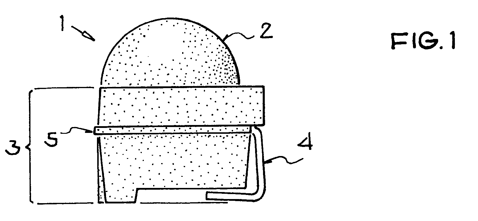
Die Fig. 1 und 2 zeigen einen Transceiver 1 mit einer Linse 2 als optisches
System, einem beispielsweise aus thermo- oder duroplastischer und für IR-Strahlen
transparenter Vergußmasse bestehenden Gehäuse 3 und Anschlußbeinchen
4, die als Teil eines metallenen Streifenträgers 5 nach außen
geführt sind. Hierbei ist das Anschlußbeinchen 4a (GND) mit dem Bezugspotential
verbunden, das Anschlußbeinchen 4b (Vcc) mit der Versorgungsspannung,
das Anschlußbeinchen 4c (RxD) mit dem Dateneingang und das
Anschlußbeinchen 4d (TxD) mit dem Datenausgang einer (nicht dargestellten)
Treiberschaltung.1 and 2 show a
Auf dem Träger 5 ist ein integrierter Schaltkreis 6 befestigt, der zur Verstärkung
der Signale dient und der Pads 7 zur Kontaktierung aufweist. Über
eine Rückseitenkontaktierung ist der integrierte Schaltkreis 6 mit dem
Masseanschluß 4a (GND) verbunden. Auf dem integrierten Schaltkreis 6 ist
eine Photo-PIN-Diode als Empfänger- oder Detektorchip 8 angeordnet, die
ebenfalls zur Kontaktierung Pads 9 aufweist. Bei dieser Photo-PIN-Diode
handelt es sich um ein spezielles IrDA-Produkt, das aber mit einer für Photo-PIN-Dioden
üblichen Technologie hergestellt ist. Um den Vorgang der
späteren Kontaktierung zu erleichtern, sind die Pads 9 vorzugsweise auf der
Vorderseite, d.h. auf der den zu empfangenden IR-Strahlen zugewandten
Seite, angeordnet. Die Oberfläche des Detektorchips 8 weist eine bis zu
seiner äußeren Begrenzung verlaufende Metallisierung 11b auf, die als
Montagefläche und Rückseitenkontakt für ein Sender- oder Emitterchip 10
und als Anschlußpad dient.An
Auf das Detektorchip 9 ist konzentrisch das Sender- oder Emitterchip 10
aufgeklebt, bei dem es sich prinzipiell um eine bekannte Infrarot-Sende-diode
handelt. Zur Kontaktierung ist eine im Zentrum des Emitterchips 10
angeordnete Kontaktfläche 11a und das mittels einer leitenden Verbindung
(Metallisierung) herausgeführte Anschlußpad 11b vorhanden.The transmitter or
Die Fläche des integrierten Schaltkreises 6 ist größer als die Fläche des
Detektorchips 8, dessen Fläche wiederum größer ist als die Fläche des
Emitterchips 10. Zur Signalübertragung erfolgt die Kontaktierung zwischen
den einzelnen Anschlußpads 7, 9, 11a bzw. 11b untereinander oder zu den
Anschlüssen 4b, 4c bzw. 4d auf bekannte Art und Weise mittels Bonddrähten
12, die aus Gold, Aluminium oder einer gut leitfähigen Legierung bestehen.The area of the integrated
Zur Befestigung des integrierten Schaltkreises 6 auf dem Träger 5, des
Detektorchips 8 auf dem integrierten Schaltkreis 6 und des Emitterchips 10
auf dem Detektorchip 8 wird beispielsweise Polymidkleber, Lot, Kunststofflot
oder ein anderer üblicher Kunststoffkleber verwendet. Um zu
gewährleisten, daß das Emitterchip 10 leitend auf dem Detektorchip 8
befestigt ist, können dabei für die einzelnen Klebungen jeweils verschiedene
Klebstoffe oder Lote Verwendung finden. Die Verbindung zwischen
dem integrierten Schaltkreis 6 und dem Detektorchip 8 kann leitfähig oder
nicht leitfähig sein, wobei der nicht leitfähigen Verbindung der Vorzug zu
geben ist.For fixing the
Das optische System 2, bei dem es sich im einfachsten Fall um eine Kunststofflinse
handelt, ist derart ausgestaltet, daß sowohl vom Emitterchip 10
ausgehende Strahlung optimal abgestrahlt wird, als auch einfallende Strahlung
optimal auf das Detektorchip 8 gelenkt wird. Ermöglicht wird dies
dadurch, daß Detektorchip 8 und Emitterchip 10 nicht wie bisher nebeneinander,
sondern übereinander angeordnet sind. Dadurch ist es möglich,
gegenüber dem Stand der Technik, bei dem jeweils für Emitter und Detektor
ein eignes optisches System verwendet werden muß, ein optisches
System einzusparen und die Breite des Transceivers 1 ungefähr zu halbieren.The
Die Fig. 3 zeigt einen Transceiver 1' nach dem Stand der Technik. Da (der
nicht sichtbare) Detektorchip und (der ebenfalls nicht sichtbare) Emitterchip
nebeneinander angeordnet sind, ist jeweils für den Emitterchip und den
Detektorchip eine eigene Linse 2' bzw. 2'' notwendig. Dadurch und daß die
Anschlüsse 4 von Detektor und Emitter getrennt herausgeführt sind, vergrößert
sich der Transceiver 1' gegenüber der erfindungsgemäßen Anordnung
auf ungefähr die doppelte Breite.3 shows a transceiver 1 ' according to the prior art. Since (the invisible) detector chip and (the likewise invisible) emitter chip are arranged next to one another, a
Claims (10)
Applications Claiming Priority (2)
| Application Number | Priority Date | Filing Date | Title |
|---|---|---|---|
| DE19727632A DE19727632C2 (en) | 1997-06-28 | 1997-06-28 | Transceiver for optical data transmission |
| DE19727632 | 1997-06-28 |
Publications (3)
| Publication Number | Publication Date |
|---|---|
| EP0903791A2 true EP0903791A2 (en) | 1999-03-24 |
| EP0903791A3 EP0903791A3 (en) | 1999-12-22 |
| EP0903791B1 EP0903791B1 (en) | 2001-11-21 |
Family
ID=7834004
Family Applications (1)
| Application Number | Title | Priority Date | Filing Date |
|---|---|---|---|
| EP98110243A Expired - Lifetime EP0903791B1 (en) | 1997-06-28 | 1998-06-05 | Apparatus for optical transmission of data |
Country Status (6)
| Country | Link |
|---|---|
| US (1) | US6320686B1 (en) |
| EP (1) | EP0903791B1 (en) |
| JP (1) | JPH1197748A (en) |
| DE (2) | DE19727632C2 (en) |
| ES (1) | ES2166119T3 (en) |
| PL (1) | PL193016B1 (en) |
Families Citing this family (14)
| Publication number | Priority date | Publication date | Assignee | Title |
|---|---|---|---|---|
| DE19823213C2 (en) * | 1998-05-25 | 2002-02-21 | Infineon Technologies Ag | Bi-directional optical transmitter and receiver |
| DE19834090A1 (en) * | 1998-07-29 | 2000-02-03 | Heidenhain Gmbh Dr Johannes | Optoelectronic transmitter and receiver unit |
| US6721503B1 (en) * | 1998-08-26 | 2004-04-13 | Georgia Tech Research Corporation | System and method for bi-directional optical communication using stacked emitters and detectors |
| US6625036B1 (en) * | 1999-08-31 | 2003-09-23 | Rohm Co., Ltd. | Infrared data communication module and method of making the same |
| JP3930710B2 (en) * | 2000-09-13 | 2007-06-13 | シチズン電子株式会社 | Chip-type light emitting diode and manufacturing method thereof |
| DE10058622A1 (en) * | 2000-11-15 | 2002-05-29 | Vishay Semiconductor Gmbh | Molded electronic component |
| DE10058608A1 (en) | 2000-11-25 | 2002-05-29 | Vishay Semiconductor Gmbh | Conductor strip arrangement for a molded electronic component and method for molding |
| US6661546B1 (en) | 2002-03-28 | 2003-12-09 | Terabeam Corporation | Multi-aperture holographic optical element for illumination sensing in a free space optical communication system |
| US6731415B1 (en) | 2002-03-28 | 2004-05-04 | Terabeam Corporation | Multi-aperture holographic optical element for use in a free space optical communication system |
| US7978800B2 (en) | 2002-10-10 | 2011-07-12 | Finisar Corporation | Circuit for converting a transponder controller chip output into an appropriate input signal for a host device |
| US7023563B2 (en) * | 2003-02-14 | 2006-04-04 | Chian Chiu Li | Interferometric optical imaging and storage devices |
| US7397022B2 (en) * | 2004-04-01 | 2008-07-08 | Vishay Semiconductor Gmbh | Sensor arrangement to prevent reference light incident on side of photodiode |
| JP4210240B2 (en) * | 2004-06-03 | 2009-01-14 | ローム株式会社 | Optical communication module |
| US7385175B2 (en) * | 2004-09-18 | 2008-06-10 | Chian Chiu Li | Bi-directional optical transmission system and method |
Family Cites Families (7)
| Publication number | Priority date | Publication date | Assignee | Title |
|---|---|---|---|---|
| DE2629356C2 (en) * | 1976-06-30 | 1983-07-21 | AEG-Telefunken Nachrichtentechnik GmbH, 7150 Backnang | Electro-optical converter for sending or receiving |
| GB2011610A (en) * | 1977-12-23 | 1979-07-11 | Elliot Bros Ltd | Fibre optic terminal |
| DE3502634A1 (en) * | 1985-01-26 | 1985-06-20 | Deutsche Forschungs- und Versuchsanstalt für Luft- und Raumfahrt e.V., 5000 Köln | OPTICAL-ELECTRONIC DISTANCE METER |
| JPH04237005A (en) * | 1991-01-22 | 1992-08-25 | Fujitsu Ltd | Photodetection module |
| US5140152A (en) * | 1991-05-31 | 1992-08-18 | The University Of Colorado Foundation, Inc. | Full duplex optoelectronic device with integral emitter/detector pair |
| US5267070A (en) * | 1992-05-05 | 1993-11-30 | The United States Of America As Represented By The Secretary Of The Navy | Underwater IR communication system |
| US5506445A (en) * | 1994-06-24 | 1996-04-09 | Hewlett-Packard Company | Optical transceiver module |
-
1997
- 1997-06-28 DE DE19727632A patent/DE19727632C2/en not_active Expired - Lifetime
-
1998
- 1998-06-04 JP JP10192238A patent/JPH1197748A/en active Pending
- 1998-06-05 EP EP98110243A patent/EP0903791B1/en not_active Expired - Lifetime
- 1998-06-05 ES ES98110243T patent/ES2166119T3/en not_active Expired - Lifetime
- 1998-06-05 DE DE59802691T patent/DE59802691D1/en not_active Expired - Lifetime
- 1998-06-10 PL PL326787A patent/PL193016B1/en unknown
- 1998-06-25 US US09/104,766 patent/US6320686B1/en not_active Expired - Lifetime
Also Published As
| Publication number | Publication date |
|---|---|
| DE59802691D1 (en) | 2002-02-21 |
| DE19727632A1 (en) | 1999-01-28 |
| PL326787A1 (en) | 1999-01-04 |
| EP0903791A3 (en) | 1999-12-22 |
| EP0903791B1 (en) | 2001-11-21 |
| DE19727632C2 (en) | 1999-10-28 |
| US6320686B1 (en) | 2001-11-20 |
| JPH1197748A (en) | 1999-04-09 |
| PL193016B1 (en) | 2007-01-31 |
| ES2166119T3 (en) | 2002-04-01 |
Similar Documents
| Publication | Publication Date | Title |
|---|---|---|
| DE19727633C2 (en) | Component for directional, bidirectional, optical data transmission | |
| EP0903791B1 (en) | Apparatus for optical transmission of data | |
| EP1095411B1 (en) | Radiation-emitting and/or -receiving component | |
| DE19549818B4 (en) | Optoelectronic semiconductor device | |
| DE3633251A1 (en) | OPTOELECTRONIC COUPLING ELEMENT | |
| DE69403622T2 (en) | Photoelectric breaker and process for its manufacture | |
| DE19536454B4 (en) | Optoelectronic semiconductor device | |
| DE10128419B4 (en) | Solid state image pickup device with microlens and underfill | |
| DE3633181A1 (en) | METHOD FOR PRODUCING AN OPTO COUPLER OR A REFLECTIVE LIGHT BARRIER AND RELATED OPTOCOUPLER OR RELATED REFLECTIVE BARRIER | |
| DE10217073A1 (en) | Optoelectronic component has optical unit arranged on upper surface of semiconducting component housing so light emission device, optical detector are connected to housing contacts | |
| DE10255625A1 (en) | Optical transceiver module and electronic device using the module | |
| DE19652030A1 (en) | Infrared transceiver and method for encapsulating the same | |
| EP0712161B1 (en) | Semiconductor assembly for a free space bidirectional optical transmission system | |
| WO2002084358A1 (en) | Emission module for an optical signal transmission | |
| EP0833764B1 (en) | Device for detecting the level of humidity on a pane | |
| DE10227544B4 (en) | Device for optical data transmission | |
| DE102007046769A1 (en) | sensor arrangement | |
| EP0875770A1 (en) | Opto-electronic sensor arrangement | |
| EP1717871A2 (en) | Optoelectronic surface-mountable component | |
| DE102010000697A1 (en) | Fiber optic transceiver (FOT) module and method for making a FOT module | |
| DE102005046164A1 (en) | X-ray detector for e.g. dental application, has base element serving as substrate/carrier for scintillation layer and photo sensor, where layer is arranged on upper side of element and sensor is arranged on lower side of element | |
| JP4486591B2 (en) | Lead terminal lead-out type electronic components | |
| EP0994509A2 (en) | Component for optically transmitting data | |
| EP3355075B1 (en) | Sensor assembly | |
| DE68920509T2 (en) | Optical module. |
Legal Events
| Date | Code | Title | Description |
|---|---|---|---|
| PUAI | Public reference made under article 153(3) epc to a published international application that has entered the european phase |
Free format text: ORIGINAL CODE: 0009012 |
|
| AK | Designated contracting states |
Kind code of ref document: A2 Designated state(s): DE ES FR GB IT |
|
| AX | Request for extension of the european patent |
Free format text: AL;LT;LV;MK;RO;SI |
|
| PUAL | Search report despatched |
Free format text: ORIGINAL CODE: 0009013 |
|
| AK | Designated contracting states |
Kind code of ref document: A3 Designated state(s): AT BE CH CY DE DK ES FI FR GB GR IE IT LI LU MC NL PT SE |
|
| AX | Request for extension of the european patent |
Free format text: AL;LT;LV;MK;RO;SI |
|
| RIC1 | Information provided on ipc code assigned before grant |
Free format text: 6H 01L 31/167 A, 6H 01L 31/147 B, 6H 01L 25/16 B, 6G 02B 6/42 B |
|
| 17P | Request for examination filed |
Effective date: 19991213 |
|
| AKX | Designation fees paid |
Free format text: DE ES FR GB IT |
|
| GRAG | Despatch of communication of intention to grant |
Free format text: ORIGINAL CODE: EPIDOS AGRA |
|
| 17Q | First examination report despatched |
Effective date: 20010320 |
|
| GRAG | Despatch of communication of intention to grant |
Free format text: ORIGINAL CODE: EPIDOS AGRA |
|
| GRAH | Despatch of communication of intention to grant a patent |
Free format text: ORIGINAL CODE: EPIDOS IGRA |
|
| ITF | It: translation for a ep patent filed | ||
| GRAH | Despatch of communication of intention to grant a patent |
Free format text: ORIGINAL CODE: EPIDOS IGRA |
|
| GRAA | (expected) grant |
Free format text: ORIGINAL CODE: 0009210 |
|
| AK | Designated contracting states |
Kind code of ref document: B1 Designated state(s): DE ES FR GB IT |
|
| REG | Reference to a national code |
Ref country code: GB Ref legal event code: IF02 |
|
| GBT | Gb: translation of ep patent filed (gb section 77(6)(a)/1977) |
Effective date: 20020121 |
|
| REF | Corresponds to: |
Ref document number: 59802691 Country of ref document: DE Date of ref document: 20020221 |
|
| REG | Reference to a national code |
Ref country code: ES Ref legal event code: FG2A Ref document number: 2166119 Country of ref document: ES Kind code of ref document: T3 |
|
| ET | Fr: translation filed | ||
| PLBE | No opposition filed within time limit |
Free format text: ORIGINAL CODE: 0009261 |
|
| STAA | Information on the status of an ep patent application or granted ep patent |
Free format text: STATUS: NO OPPOSITION FILED WITHIN TIME LIMIT |
|
| 26N | No opposition filed | ||
| REG | Reference to a national code |
Ref country code: FR Ref legal event code: PLFP Year of fee payment: 19 |
|
| REG | Reference to a national code |
Ref country code: FR Ref legal event code: PLFP Year of fee payment: 20 |
|
| PGFP | Annual fee paid to national office [announced via postgrant information from national office to epo] |
Ref country code: FR Payment date: 20170621 Year of fee payment: 20 Ref country code: GB Payment date: 20170620 Year of fee payment: 20 Ref country code: DE Payment date: 20170621 Year of fee payment: 20 |
|
| PGFP | Annual fee paid to national office [announced via postgrant information from national office to epo] |
Ref country code: IT Payment date: 20170622 Year of fee payment: 20 |
|
| PGFP | Annual fee paid to national office [announced via postgrant information from national office to epo] |
Ref country code: ES Payment date: 20170724 Year of fee payment: 20 |
|
| REG | Reference to a national code |
Ref country code: DE Ref legal event code: R071 Ref document number: 59802691 Country of ref document: DE |
|
| REG | Reference to a national code |
Ref country code: GB Ref legal event code: PE20 Expiry date: 20180604 |
|
| PG25 | Lapsed in a contracting state [announced via postgrant information from national office to epo] |
Ref country code: GB Free format text: LAPSE BECAUSE OF EXPIRATION OF PROTECTION Effective date: 20180604 |
|
| REG | Reference to a national code |
Ref country code: ES Ref legal event code: FD2A Effective date: 20220103 |
|
| PG25 | Lapsed in a contracting state [announced via postgrant information from national office to epo] |
Ref country code: ES Free format text: LAPSE BECAUSE OF EXPIRATION OF PROTECTION Effective date: 20180606 |