EP0902977B1 - Oberflächenmontiertes gehäuse mit wärmeübertragungseigenschaften - Google Patents
Oberflächenmontiertes gehäuse mit wärmeübertragungseigenschaften Download PDFInfo
- Publication number
- EP0902977B1 EP0902977B1 EP97927681A EP97927681A EP0902977B1 EP 0902977 B1 EP0902977 B1 EP 0902977B1 EP 97927681 A EP97927681 A EP 97927681A EP 97927681 A EP97927681 A EP 97927681A EP 0902977 B1 EP0902977 B1 EP 0902977B1
- Authority
- EP
- European Patent Office
- Prior art keywords
- substrate
- areas
- conducting
- electronic package
- top surface
- Prior art date
- Legal status (The legal status is an assumption and is not a legal conclusion. Google has not performed a legal analysis and makes no representation as to the accuracy of the status listed.)
- Expired - Lifetime
Links
Images

Classifications
-
- H—ELECTRICITY
- H01—ELECTRIC ELEMENTS
- H01L—SEMICONDUCTOR DEVICES NOT COVERED BY CLASS H10
- H01L25/00—Assemblies consisting of a plurality of semiconductor or other solid state devices
- H01L25/03—Assemblies consisting of a plurality of semiconductor or other solid state devices all the devices being of a type provided for in a single subclass of subclasses H10B, H10D, H10F, H10H, H10K or H10N, e.g. assemblies of rectifier diodes
- H01L25/04—Assemblies consisting of a plurality of semiconductor or other solid state devices all the devices being of a type provided for in a single subclass of subclasses H10B, H10D, H10F, H10H, H10K or H10N, e.g. assemblies of rectifier diodes the devices not having separate containers
- H01L25/07—Assemblies consisting of a plurality of semiconductor or other solid state devices all the devices being of a type provided for in a single subclass of subclasses H10B, H10D, H10F, H10H, H10K or H10N, e.g. assemblies of rectifier diodes the devices not having separate containers the devices being of a type provided for in group subclass H10D
- H01L25/072—Assemblies consisting of a plurality of semiconductor or other solid state devices all the devices being of a type provided for in a single subclass of subclasses H10B, H10D, H10F, H10H, H10K or H10N, e.g. assemblies of rectifier diodes the devices not having separate containers the devices being of a type provided for in group subclass H10D the devices being arranged next to each other
-
- H—ELECTRICITY
- H01—ELECTRIC ELEMENTS
- H01L—SEMICONDUCTOR DEVICES NOT COVERED BY CLASS H10
- H01L2224/00—Indexing scheme for arrangements for connecting or disconnecting semiconductor or solid-state bodies and methods related thereto as covered by H01L24/00
- H01L2224/01—Means for bonding being attached to, or being formed on, the surface to be connected, e.g. chip-to-package, die-attach, "first-level" interconnects; Manufacturing methods related thereto
- H01L2224/42—Wire connectors; Manufacturing methods related thereto
- H01L2224/47—Structure, shape, material or disposition of the wire connectors after the connecting process
- H01L2224/48—Structure, shape, material or disposition of the wire connectors after the connecting process of an individual wire connector
- H01L2224/481—Disposition
- H01L2224/48151—Connecting between a semiconductor or solid-state body and an item not being a semiconductor or solid-state body, e.g. chip-to-substrate, chip-to-passive
- H01L2224/48221—Connecting between a semiconductor or solid-state body and an item not being a semiconductor or solid-state body, e.g. chip-to-substrate, chip-to-passive the body and the item being stacked
- H01L2224/48225—Connecting between a semiconductor or solid-state body and an item not being a semiconductor or solid-state body, e.g. chip-to-substrate, chip-to-passive the body and the item being stacked the item being non-metallic, e.g. insulating substrate with or without metallisation
- H01L2224/48227—Connecting between a semiconductor or solid-state body and an item not being a semiconductor or solid-state body, e.g. chip-to-substrate, chip-to-passive the body and the item being stacked the item being non-metallic, e.g. insulating substrate with or without metallisation connecting the wire to a bond pad of the item
-
- H—ELECTRICITY
- H01—ELECTRIC ELEMENTS
- H01L—SEMICONDUCTOR DEVICES NOT COVERED BY CLASS H10
- H01L2924/00—Indexing scheme for arrangements or methods for connecting or disconnecting semiconductor or solid-state bodies as covered by H01L24/00
- H01L2924/30—Technical effects
- H01L2924/301—Electrical effects
- H01L2924/30107—Inductance
-
- H—ELECTRICITY
- H01—ELECTRIC ELEMENTS
- H01L—SEMICONDUCTOR DEVICES NOT COVERED BY CLASS H10
- H01L2924/00—Indexing scheme for arrangements or methods for connecting or disconnecting semiconductor or solid-state bodies as covered by H01L24/00
- H01L2924/30—Technical effects
- H01L2924/301—Electrical effects
- H01L2924/3011—Impedance
-
- H—ELECTRICITY
- H05—ELECTRIC TECHNIQUES NOT OTHERWISE PROVIDED FOR
- H05K—PRINTED CIRCUITS; CASINGS OR CONSTRUCTIONAL DETAILS OF ELECTRIC APPARATUS; MANUFACTURE OF ASSEMBLAGES OF ELECTRICAL COMPONENTS
- H05K1/00—Printed circuits
- H05K1/02—Details
- H05K1/0213—Electrical arrangements not otherwise provided for
- H05K1/0237—High frequency adaptations
-
- H—ELECTRICITY
- H05—ELECTRIC TECHNIQUES NOT OTHERWISE PROVIDED FOR
- H05K—PRINTED CIRCUITS; CASINGS OR CONSTRUCTIONAL DETAILS OF ELECTRIC APPARATUS; MANUFACTURE OF ASSEMBLAGES OF ELECTRICAL COMPONENTS
- H05K3/00—Apparatus or processes for manufacturing printed circuits
- H05K3/30—Assembling printed circuits with electric components, e.g. with resistor
- H05K3/32—Assembling printed circuits with electric components, e.g. with resistor electrically connecting electric components or wires to printed circuits
- H05K3/34—Assembling printed circuits with electric components, e.g. with resistor electrically connecting electric components or wires to printed circuits by soldering
- H05K3/341—Surface mounted components
- H05K3/3431—Leadless components
Definitions
- a known electronic package disclosed by US 4,739,448 comprises an electronic chip, bond wires connecting the chip to conducting output areas on a top surface of an insulating substrate, conducting vias through the substrate connecting the output areas to respective pads on a bottom surface of the substrate, the chip being mounted on a conducting common area on the top surface, and a further conducting via through the substrate connecting the common area and a heat transfer pad on the bottom surface.
- the conducting via conducts heat from the common area through the substrate, which provides thermal dissipation to remove heat from the chip.
- diodes for RF transmit applications would require a package with improved thermal dissipation to keep insertion losses low, and to maintain reliable operation over time.
- a problem associated with an electronic package is an inability of the package to dissipate heat from diodes.
- the invention provides an electronic package with improved thermal dissipation.
- the invention is characterised by conducting heat spreading areas on the top surface of the substrate, the heat spreading areas being separated from the common area by slender gaps, the heat spreading areas being disconnected from said bond wires and said conducting output areas, and multiple conducting vias connecting the heat spreading areas to a heat conducting, surface mount, ground pad on the bottom surface of the substrate.
- the heat spreading areas are unlike the two conducting areas, as disclosed by US 5,424,693, which conducting areas are on the top of the substrate to add capacitance coupling to the signal output areas.
- the package (1) is adapted for mounting on a circuit board.
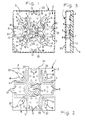
- the package (1) for diodes comprises, a flat substrate (2) of known alumina material having a top surface (3) and a bottom surface (4).
- a common area (5) on the top surface (3) is constructed of metallic conducting material known as metallization, such as copper as an underlayment that is covered by a flash of precious metal, such as gold.
- the common area (5) provides a mounting surface on which at least one diode (6), or alternatively, multiple diodes (6), can be mounted and electrically attached to a conducting common port, such as by corresponding epoxy attach or solder joints (7), Figs. 3 and 6, to the common area (5).
- Each of the diodes (6) is a discrete PIN diode chip, for example, available from M/A-COM Inc., 1011 Pawtucket Boulevard, Lowell MA 01853, USA, Part Number FN00008 or MA4PC723-2 and MA4PC723-4.
- Other suggested sources of supply exist for the equivalent part numbers. For example, Alpha Industries, 20 Sylvan Road, Woburn, MA 01801, USA, and Loral Microwave -FSI, Semiconductor Division, 16 Maple Road, Chelmsford, MA 01824., USA.
- a metallization is known, in the field of package manufacturing, to comprise, a layer of conducting material applied to a surface of a substrate, such as the substrate (2), by deposition techniques that include plating, printing and vapor deposition, for example.
- a metallization is a conducting layer of sufficient thickness to withstand a process of attachment thereto of a bond wire or a solder joint, or of a sufficient thickness to promote heat conduction and spreading.
- bond wires (8) extend from respective active areas on the diodes (6) to connect with respective conducting output areas (9) on the top surface (3).
- the output areas (9) are also metallization, such as copper, as an underlayment, covered and adhered to by a flash of precious metal, such as gold.
- thick film gold pads (10) are applied to a portion of the gold flash, to which respective bond wires (8) are attached.
- a dam (11) is provided by an insulating strip of glass deposited as an overglaze that extends across the corresponding output area (9) to divide the output area (9) into two surface portions.
- Each dam (11) resists wicking and spreading of the thick film gold as it is being applied, and thus confines an outer edge of the corresponding thick film gold pad (10) to the portion of the output area. Accordingly, gold consumption is reduced.
- the thick film gold pads (10) are designed to be short 50 Ohm thick film transmission lines, with the adjacent ground areas (21) assisting to control the impedance of the thick film transmission lines.
- Thick film capacitor pads (12) are on the top surface (3) of the substrate (2), adjacent to respective output areas (9). Wire bonds (8) connect the capacitor pads (12) with the thick film gold, output areas (9) to compensate for inductance in the bond wires (8) extending from respective diodes (6).
- the common area (5) is connected by at least one conducting via (13) to a surface mount pad, more particularly, a common pad (14), on the bottom surface (4) of the substrate (2).
- a surface mount pad more particularly, a common pad (14), on the bottom surface (4) of the substrate (2).
- each via (13), with reference to Fig. 7, is an aperture (15) through the substrate (2), lined with conductive plating (16), and extending from the top surface (3) to the bottom surface (4).
- Each aperture (15) is filled with a sealant (17), epoxy, for example, thereby to seal the top surface (3) from the bottom surface (4).
- adjacent diodes (6) are separated by a 0.0076cm (0.003 inch) gap that is centered on the common area (5).
- the adjacent diodes (6) are equidistant from a via (13).
- each of the diodes (6) is approximately .013 to .018 inches, 0.033 to 0.046 cm, square, and is approximately .005 to .012 inches, 0.003 to 0.030 cm, in height.
- two diodes (6) can be joined to the same gold pad (10) of an output area (9) when increased power output is desired.
- Each of the output areas (9) is connected by at least one conducting via (13) to respective surface mount pads, more particularly, output pads (18), Figs. 2 and 5, on the bottom surface (4) of the substrate (2).
- Heat spreading areas (19) on the top surface (3) of the substrate (2) are constructed as metallization, for example, copper, covered by a flash of gold.
- the heat spreading areas (19) are separated from the common area (5) by slender gaps, across which heat transfer occurs.
- Alumina is heat conductive to transfer heat across the gaps to the heat spreading areas (19).
- Multiple conducting vias (13) connect each of the heat spreading areas (19) that are shown in the drawings as being disconnected from said bond wires (8) and said conducting output areas (9), to a corresponding heat conducting, surface mount pad, more particularly, a ground pad (20) on the bottom surface (4) of the substrate (2).
- the ground pad (20) is larger in area than the combined area of the heat spreading areas (19), so as to dissipate heat over a large surface.
- Heat from the diodes (6) also transfers through the thickness of the alumina substrate (2) to the ground pad (20), the alumina having a thickness on the order of 0.015 to 0.025 inch, 3.81 - 6.35 mm.
- a ground area (21) of metallization for example, copper covered by a flash of gold, is interposed between each pair of output areas (9).
- the ground areas (21) insure electrical isolation of the output areas (9).
- the ground areas (21) are between capacitor pads (12), providing electrical isolation.
- Multiple connecting vias (13) connect each of the ground areas (21) to the corresponding heat conducting, ground pad (20) on the bottom surface (4) of the substrate (2).
- Each of the surface mount pads (14, 18, 20) provides a corresponding electrical terminal for connection to a circuit board, for example, by solder connection of the surface mount pads (14, 18, 20), in a known manner, to a circuit board.
- Each of the pads (14, 18) is separated by a dam (11) from the ground pad (20).
- the dams (11) are fabricated of insulating material, for example, glass deposited as an overglaze on the bottom surface (4) of the substrate (2). The purpose of the dams (11) is to resist wicking or splashing of copper and gold materials used in the fabrication of the pads (14, 18, 20), and to prevent wicking of solder that is used for connection of the pads (14, 18, 20) to a circuit board.
- electrical isolation of the surface mount pads (14, 18) is provided, for example, by the heat conducting, surface mount ground pad (20) encircling the common pad (14) that is connected to the common area (5), and by the heat conducting, surface mount pad (20) being interposed between the common pad (14) and each of the output pads (18).
- Glass dams applied as an overglaze, extend in narrow strips along gaps between the heat conducting ground surface mount pad and each of the other surface mount pads. During deposition of copper and gold flash that forms the conducting pads, the dams prevent adhesion of copper and splashing and wicking of the metallization to assure that gaps are maintained for electrical separation of the pads from one another.
- each of the surface mount pads (14, 18, 20) is provided with a unitary tab (22) that extends to provide a unique pattern of tabs (22) that assists in orientation of the bottom surface (4) during manufacture and assembly of the package.
- a tab (22) is unitary with each of the ground areas (21), and each of the heat spreading areas (19), and extends to a corresponding edge margin of the top surface (3) of the substrate (2) to provide a unique pattern of tabs (22) that assists in orientation of the substrate (2) during manufacture and assembly of the package (1).
- a hollow cover (23) is attached to the edge margin on the top surface (3) of the substrate (2), and encloses the top surface of the substrate.
- the hollow cover (23) eliminates encapsulant material and its accompanying capacitance.
- Edges of the hollow cover (23) are joined with adhesive, for example, BSE-1 B-stage epoxy, approximately 51 ⁇ m (2 mils). thick, to edge margins of the substrate (2) along the top surface (3).
- adhesive for example, BSE-1 B-stage epoxy, approximately 51 ⁇ m (2 mils). thick, to edge margins of the substrate (2) along the top surface (3).
- the cover (23) is available from Robison Electronics, Inc., 3580 Sacramento Drive, San Luis Obispo, CA 93403, USA part numbers, VSC- 250100S4, VOC-150250S2 and VSC-150100S2.
- the cover (23) has a height of about 0.100 inches, 0.254 cm, and covers a rectangular area bounded by sides having lengths of 0.150 inches, 0.381 cm, or 0.250 inches, 0.635 cm, in any combination of such lengths.
- An advantage of the invention resides in a package of diodes (6) with improved heat conduction and controlled inductance.
Landscapes
- Engineering & Computer Science (AREA)
- Power Engineering (AREA)
- Microelectronics & Electronic Packaging (AREA)
- Physics & Mathematics (AREA)
- Condensed Matter Physics & Semiconductors (AREA)
- General Physics & Mathematics (AREA)
- Computer Hardware Design (AREA)
- Cooling Or The Like Of Semiconductors Or Solid State Devices (AREA)
- Structures For Mounting Electric Components On Printed Circuit Boards (AREA)
Claims (8)
- Elektronische Baugruppe (1), die aufweist: einen Träger (2) aus Aluminiumoxid; eine leitende gemeinsame Fläche (5) auf einer oberen Fläche (3) des Trägers (2) für ein leitendes Montieren einer oder mehrerer Dioden (6); Verbindungsdrähte (8), die stromführende Flächen auf den Dioden (6) mit leitenden Ausgangsflächen (9) auf der oberen Fläche (3) verbinden; und leitende Durchgänge (13, 13) durch den Träger (2), die die gemeinsame Fläche (5) und die Ausgangsflächen (9) mit entsprechenden Oberflächenmontageanschlußflächen (14, 18) auf einer unteren Fläche (4) des Trägers (2) verbinden, wobei die elektronische Baugruppe (1) gekennzeichnet ist durch:leitende Wärmeverteilungsflächen (19) auf der oberen Fläche (3) des Trägers (2), wobei die Wärmeverteilungsflächen (19) von der gemeinsamen Fläche (5) durch schmale Spalten getrennt sind, wobei die Wärmeverteilungsflächen (19) von den Verbindungsdrähten (8) und den leitenden Ausgangsflächen (9) getrennt sind; und mehrere leitende Durchgänge (13), die jede der Wärmeverteilungsflächen (19) mit einer wärmeleitenden Oberflächenmontageerdungsanschlußfläche (20) auf der unteren Fläche (4) des Trägers (2) verbinden.
- Elektronische Baugruppe (1) nach Anspruch 1, bei der jede Ausgangsfläche (9) aufweist: eine Kupferunterlage; eine Hauchvergoldung, die an der Unterlage haftet; und Dickschichtgoldanschlußflächen (10), die auf einem Abschnitt der Hauchvergoldung aufgebracht werden, an denen entsprechende Verbindungsdrähte (8) befestigt werden.
- Elektronische Baugruppe (1) nach Anspruch 2, bei der sich ein Isolierstreifen (11) über jede Ausgangsfläche (9) erstreckt, um einen Rand der Dickschichtgoldanschlußfläche (10) auf dem Abschnitt der Hauchvergoldung zu begrenzen.
- Elektronische Baugruppe (1) nach Anspruch 1, bei der eine zusätzliche Erdungsfläche (21) auf der oberen Fläche (3) zwischen den Ausgangsflächen (9) vorhanden ist, wobei die zusätzliche Erdungsfläche (21) eine elektrische Isolierung bewirkt.
- Elektronische Baugruppe (1) nach Anspruch 2, bei der Dickschichtkondensatoranschlußflächen (12) auf der oberen Fläche (3) des Trägers (2) vorhanden sind und weitere Verbindungsdrähte (8) die Dickschichtgoldanschlußflächen (10) mit den Kondensatoranschlußflächen (12) verbinden, um eine Induktivität in den Verbindungsdrähten (8) zu kompensieren.
- Elektronische Baugruppe (1) nach Anspruch 5, bei der eine zusätzliche Erdungsfläche (21) auf der oberen Fläche (3) zwischen den Kondensatoranschlußflächen (12) vorhanden ist, wobei die zusätzliche Erdungsfläche (21) eine elektrische Isolierung bewirkt.
- Elektronische Baugruppe (1) nach Anspruch 1, bei der eine hohle Abdeckkappe (23) am Träger (2) befestigt ist und die obere Fläche (3) des Trägers (2) einschließt.
- Elektronische Baugruppe (1) nach Anspruch 1, bei der jeder Durchgang (13) eine galvanisch beschichtete Öffnung (15) durch eine Dicke des Trägers (2) hindurch und ein Epoxidharz (17) aufweist, das die Öffnung (15) ausfüllt.
Applications Claiming Priority (3)
| Application Number | Priority Date | Filing Date | Title |
|---|---|---|---|
| US646802 | 1996-05-21 | ||
| US08/646,802 US5679979A (en) | 1996-05-21 | 1996-05-21 | Surface mount package with heat transfer feature |
| PCT/US1997/008592 WO1997044825A1 (en) | 1996-05-21 | 1997-05-21 | Surface mount package with heat transfer feature |
Publications (2)
| Publication Number | Publication Date |
|---|---|
| EP0902977A1 EP0902977A1 (de) | 1999-03-24 |
| EP0902977B1 true EP0902977B1 (de) | 2002-03-06 |
Family
ID=24594519
Family Applications (1)
| Application Number | Title | Priority Date | Filing Date |
|---|---|---|---|
| EP97927681A Expired - Lifetime EP0902977B1 (de) | 1996-05-21 | 1997-05-21 | Oberflächenmontiertes gehäuse mit wärmeübertragungseigenschaften |
Country Status (5)
| Country | Link |
|---|---|
| US (1) | US5679979A (de) |
| EP (1) | EP0902977B1 (de) |
| JP (1) | JP3648252B2 (de) |
| DE (1) | DE69710885T2 (de) |
| WO (1) | WO1997044825A1 (de) |
Families Citing this family (3)
| Publication number | Priority date | Publication date | Assignee | Title |
|---|---|---|---|---|
| TW328645B (en) * | 1997-04-14 | 1998-03-21 | Chyng-Guang Juang | The package for dual mode micro/nano-meter wave IC |
| US6437381B1 (en) | 2000-04-27 | 2002-08-20 | International Business Machines Corporation | Semiconductor memory device with reduced orientation-dependent oxidation in trench structures |
| DE10316136A1 (de) * | 2003-04-09 | 2004-11-18 | Ixys Semiconductor Gmbh | Gekapselte Leistungshalbleiteranordnung |
Family Cites Families (22)
| Publication number | Priority date | Publication date | Assignee | Title |
|---|---|---|---|---|
| JPS5129636B1 (de) * | 1970-12-25 | 1976-08-26 | ||
| JPS5412284A (en) * | 1977-06-28 | 1979-01-29 | Mitsubishi Electric Corp | Photo coupled semiconductor device |
| US5014159A (en) * | 1982-04-19 | 1991-05-07 | Olin Corporation | Semiconductor package |
| JPS58199573A (ja) * | 1982-05-17 | 1983-11-19 | Hitachi Ltd | 半導体装置 |
| JPS59105392A (ja) * | 1982-12-08 | 1984-06-18 | Hitachi Ltd | 半導体レ−ザ−装置 |
| US4739448A (en) * | 1984-06-25 | 1988-04-19 | Magnavox Government And Industrial Electronics Company | Microwave multiport multilayered integrated circuit chip carrier |
| JPS63142684A (ja) * | 1986-12-05 | 1988-06-15 | Hitachi Ltd | 発光ダイオ−ド装置 |
| US4847848A (en) * | 1987-02-20 | 1989-07-11 | Sanyo Electric Co., Ltd. | Semiconductor laser device |
| US5045914A (en) * | 1989-12-26 | 1991-09-03 | Motorola, Inc. | Plastic pad array electronic AC device |
| US5132875A (en) * | 1990-10-29 | 1992-07-21 | Compaq Computer Corporation | Removable protective heat sink for electronic components |
| JP2695995B2 (ja) * | 1991-01-14 | 1998-01-14 | 株式会社東芝 | 光半導体装置 |
| JP2728322B2 (ja) * | 1991-09-05 | 1998-03-18 | 三菱電機株式会社 | 半導体装置 |
| JPH0567768A (ja) * | 1991-09-06 | 1993-03-19 | Hitachi Ltd | 光電子装置 |
| US5262927A (en) * | 1992-02-07 | 1993-11-16 | Lsi Logic Corporation | Partially-molded, PCB chip carrier package |
| FI91136C (fi) * | 1992-07-03 | 1994-05-25 | Kauko Rautio | Pyöröterän kiinnitysjärjestelmä |
| DE59304797D1 (de) * | 1992-08-26 | 1997-01-30 | Eupec Gmbh & Co Kg | Leistungshalbleiter-Modul |
| US5280409A (en) * | 1992-10-09 | 1994-01-18 | Sun Microsystems, Inc. | Heat sink and cover for tab integrated circuits |
| US5424693A (en) * | 1993-01-13 | 1995-06-13 | Industrial Technology Research Institute | Surface mountable microwave IC package |
| JPH07263871A (ja) * | 1994-03-18 | 1995-10-13 | Fujitsu Ltd | プリント配線板 |
| US5463250A (en) * | 1994-04-29 | 1995-10-31 | Westinghouse Electric Corp. | Semiconductor component package |
| US5521406A (en) * | 1994-08-31 | 1996-05-28 | Texas Instruments Incorporated | Integrated circuit with improved thermal impedance |
| US5513070A (en) * | 1994-12-16 | 1996-04-30 | Intel Corporation | Dissipation of heat through keyboard using a heat pipe |
-
1996
- 1996-05-21 US US08/646,802 patent/US5679979A/en not_active Expired - Lifetime
-
1997
- 1997-05-21 WO PCT/US1997/008592 patent/WO1997044825A1/en not_active Ceased
- 1997-05-21 JP JP54267797A patent/JP3648252B2/ja not_active Expired - Fee Related
- 1997-05-21 EP EP97927681A patent/EP0902977B1/de not_active Expired - Lifetime
- 1997-05-21 DE DE69710885T patent/DE69710885T2/de not_active Expired - Fee Related
Also Published As
| Publication number | Publication date |
|---|---|
| EP0902977A1 (de) | 1999-03-24 |
| DE69710885D1 (de) | 2002-04-11 |
| US5679979A (en) | 1997-10-21 |
| DE69710885T2 (de) | 2002-09-19 |
| WO1997044825A1 (en) | 1997-11-27 |
| JP2000516393A (ja) | 2000-12-05 |
| JP3648252B2 (ja) | 2005-05-18 |
Similar Documents
| Publication | Publication Date | Title |
|---|---|---|
| EP1304909B1 (de) | Hochfrequenz-Halbleitervorrichtung | |
| US5715144A (en) | Multi-layer, multi-chip pyramid and circuit board structure | |
| US5907903A (en) | Multi-layer-multi-chip pyramid and circuit board structure and method of forming same | |
| US6020637A (en) | Ball grid array semiconductor package | |
| US5367435A (en) | Electronic package structure and method of making same | |
| US5578525A (en) | Semiconductor device and a fabrication process thereof | |
| US6154372A (en) | Multichip module for surface mounting on printed circuit boards | |
| US5661089A (en) | Method for making a semiconductor chip package with enhanced thermal conductivity | |
| KR970067892A (ko) | 고주파 집적회로장치 및 그 제조방법 | |
| US5869889A (en) | Thin power tape ball grid array package | |
| US6323065B1 (en) | Methods for manufacturing ball grid array assembly semiconductor packages | |
| US5434357A (en) | Reduced semiconductor size package | |
| US6150716A (en) | Metal substrate having an IC chip and carrier mounting | |
| US6034437A (en) | Semiconductor device having a matrix of bonding pads | |
| EP0817266B1 (de) | Montagestruktur für eine integrierte Schaltung | |
| US4538143A (en) | Light-emitting diode displayer | |
| US6351389B1 (en) | Device and method for packaging an electronic device | |
| EP0902977B1 (de) | Oberflächenmontiertes gehäuse mit wärmeübertragungseigenschaften | |
| JP3312611B2 (ja) | フィルムキャリア型半導体装置 | |
| KR100658120B1 (ko) | 필름 기판을 사용한 반도체 장치 제조 방법 | |
| GB2301937A (en) | IC package with a ball grid array on a single layer ceramic substrate | |
| JP2636602B2 (ja) | 半導体装置 | |
| JPH07115281A (ja) | プリント配線板 | |
| KR20000044989A (ko) | 멀티 칩 볼 그리드 어레이 패키지 | |
| KR19990013776A (ko) | 반도체 장치 |
Legal Events
| Date | Code | Title | Description |
|---|---|---|---|
| PUAI | Public reference made under article 153(3) epc to a published international application that has entered the european phase |
Free format text: ORIGINAL CODE: 0009012 |
|
| 17P | Request for examination filed |
Effective date: 19981211 |
|
| AK | Designated contracting states |
Kind code of ref document: A1 Designated state(s): DE FR GB |
|
| GRAG | Despatch of communication of intention to grant |
Free format text: ORIGINAL CODE: EPIDOS AGRA |
|
| 17Q | First examination report despatched |
Effective date: 20010514 |
|
| GRAG | Despatch of communication of intention to grant |
Free format text: ORIGINAL CODE: EPIDOS AGRA |
|
| GRAH | Despatch of communication of intention to grant a patent |
Free format text: ORIGINAL CODE: EPIDOS IGRA |
|
| GRAH | Despatch of communication of intention to grant a patent |
Free format text: ORIGINAL CODE: EPIDOS IGRA |
|
| REG | Reference to a national code |
Ref country code: GB Ref legal event code: IF02 |
|
| GRAA | (expected) grant |
Free format text: ORIGINAL CODE: 0009210 |
|
| AK | Designated contracting states |
Kind code of ref document: B1 Designated state(s): DE FR GB |
|
| REF | Corresponds to: |
Ref document number: 69710885 Country of ref document: DE Date of ref document: 20020411 |
|
| ET | Fr: translation filed | ||
| PLBE | No opposition filed within time limit |
Free format text: ORIGINAL CODE: 0009261 |
|
| STAA | Information on the status of an ep patent application or granted ep patent |
Free format text: STATUS: NO OPPOSITION FILED WITHIN TIME LIMIT |
|
| 26N | No opposition filed |
Effective date: 20021209 |
|
| REG | Reference to a national code |
Ref country code: GB Ref legal event code: 732E Free format text: REGISTERED BETWEEN 20090319 AND 20090325 |
|
| PGFP | Annual fee paid to national office [announced via postgrant information from national office to epo] |
Ref country code: FR Payment date: 20090518 Year of fee payment: 13 Ref country code: DE Payment date: 20090528 Year of fee payment: 13 |
|
| REG | Reference to a national code |
Ref country code: FR Ref legal event code: TP |
|
| PGFP | Annual fee paid to national office [announced via postgrant information from national office to epo] |
Ref country code: GB Payment date: 20090528 Year of fee payment: 13 |
|
| REG | Reference to a national code |
Ref country code: GB Ref legal event code: 732E Free format text: REGISTERED BETWEEN 20100114 AND 20100120 |
|
| REG | Reference to a national code |
Ref country code: FR Ref legal event code: TP |
|
| GBPC | Gb: european patent ceased through non-payment of renewal fee |
Effective date: 20100521 |
|
| REG | Reference to a national code |
Ref country code: FR Ref legal event code: ST Effective date: 20110131 |
|
| PG25 | Lapsed in a contracting state [announced via postgrant information from national office to epo] |
Ref country code: DE Free format text: LAPSE BECAUSE OF NON-PAYMENT OF DUE FEES Effective date: 20101201 |
|
| PG25 | Lapsed in a contracting state [announced via postgrant information from national office to epo] |
Ref country code: FR Free format text: LAPSE BECAUSE OF NON-PAYMENT OF DUE FEES Effective date: 20100531 |
|
| PG25 | Lapsed in a contracting state [announced via postgrant information from national office to epo] |
Ref country code: GB Free format text: LAPSE BECAUSE OF NON-PAYMENT OF DUE FEES Effective date: 20100521 |