EP0902525A2 - Verfahren und Vorrichtung zur Verminderung der Stromversorgungsstromspitzen in einer Ladungspumpe durch die Anwendung eines verzögerten Taktsignals - Google Patents
Verfahren und Vorrichtung zur Verminderung der Stromversorgungsstromspitzen in einer Ladungspumpe durch die Anwendung eines verzögerten Taktsignals Download PDFInfo
- Publication number
- EP0902525A2 EP0902525A2 EP98307090A EP98307090A EP0902525A2 EP 0902525 A2 EP0902525 A2 EP 0902525A2 EP 98307090 A EP98307090 A EP 98307090A EP 98307090 A EP98307090 A EP 98307090A EP 0902525 A2 EP0902525 A2 EP 0902525A2
- Authority
- EP
- European Patent Office
- Prior art keywords
- charge pump
- clock
- circuit
- coupled
- charge
- Prior art date
- Legal status (The legal status is an assumption and is not a legal conclusion. Google has not performed a legal analysis and makes no representation as to the accuracy of the status listed.)
- Withdrawn
Links
Images



Classifications
-
- H—ELECTRICITY
- H02—GENERATION; CONVERSION OR DISTRIBUTION OF ELECTRIC POWER
- H02M—APPARATUS FOR CONVERSION BETWEEN AC AND AC, BETWEEN AC AND DC, OR BETWEEN DC AND DC, AND FOR USE WITH MAINS OR SIMILAR POWER SUPPLY SYSTEMS; CONVERSION OF DC OR AC INPUT POWER INTO SURGE OUTPUT POWER; CONTROL OR REGULATION THEREOF
- H02M3/00—Conversion of DC power input into DC power output
- H02M3/02—Conversion of DC power input into DC power output without intermediate conversion into AC
- H02M3/04—Conversion of DC power input into DC power output without intermediate conversion into AC by static converters
- H02M3/06—Conversion of DC power input into DC power output without intermediate conversion into AC by static converters using resistors or capacitors, e.g. potential divider
- H02M3/07—Conversion of DC power input into DC power output without intermediate conversion into AC by static converters using resistors or capacitors, e.g. potential divider using capacitors charged and discharged alternately by semiconductor devices with control electrode, e.g. charge pumps
Definitions
- the present invention relates to charge pumps, and methods and apparatus for reducing power supply current surges in a charge Pump.
- Patent number 5,629,890 to Engh relates to an integrated circuit system for analog signal storage which incorporates a read-while-write programming method.
- a high voltage ramp is applied to a memory cell to program the memory cell to a target voltage.
- Figure 1 illustrates the charge pump circuit 100 that provides the high output voltage during writing/programming of a memory cell.
- the charge pump circuit 100 includes two charge pump lines, each charge pump line having a plurality of charge pump stages 110A 1 -110A n and 110B 1 -110B n , respectively.
- Each of the charge pump stages 110A 1 -110A n and 110B 1 -110B n includes a respective capacitor CA 1 -CA n and CB 1 -CB n , and a respective N-channel device MA 1 -MA n and MB 1 -MB n , each connected as a diode.
- a plurality of clock sources CLK1, CLK1B, CLK2, and CLK2B are provided, with alternate stages of each charge pump being connected to a common clock signal.
- FIG 2A illustrates a timing diagram of the prior art charge pump clock signals.
- clock signals CLK1 and CLK1B as well as clock signals CLK2 and CLK2B, are non-overlapping.
- clock signals CLK1 and CLK1B are never both high at the same time
- clock signals CLK2 and CLK2B are never both high at the same time.
- the operation of the circuit of Figure 1 may be described as follows.
- diode-connected transistor MA 2 will be just on the threshold of conducting, though no substantial charge will be transferred from capacitor CA 1 to capacitor CA2.
- clock signal CLK1 goes low again, diode-connected transistor MA 1 will be reverse biased.
- clock signal CLK1B goes high, the voltage on node A 1 will increase from 2V dd -2V d toward 3V dd -2V d . If at this time the voltage on node A 2 is less than 3V dd -3V d , part of the charge from capacitor CA 2 will be dumped into capacitor CA 3 .
- output capacitor CA n and CB n will discharge somewhat between pumping cycles to provide the output current into the load, in which case each stage of the two charge pump lines will pump charge toward the output at a rate dependent upon the charge pump output current. Accordingly, the charge pump circuit will appear as a voltage source with a source impedance inversely proportional to the size of the capacitors times the frequency of the clock signals.
- a read operation is simultaneously performed while the memory cell is being programmed to determine when to terminate the application of the high voltage (i.e., when the target voltage is reached). Since the reading occurs during the writing operation, the charge pump circuit 100 of Figure 1 is active when the voltage stored on the cell is being read back.
- the loading on each of the clock drivers of the prior art is relatively large, being proportional to (n*C)/2, where n is the number of charge pump stages and C is the value of each capacitor.
- Driving a large load requires a large clock driver, which in turn increases the demand on the power supply. Large demands on the power supply cause current surges which cause undesirable disturbances in the system.
- Figure 2B schematically illustrates the current surges on the power supply with reference to clocks CLK1, CLK1B, CLK2, and CLK2B.
- the present invention is a charge pump circuit to reduce and distribute power supply current surges.
- the charge pump circuit includes a first clock line to provide a first clock thereon, a plurality of delay circuits connected in series, each delay circuit generating a delayed and inverted clock from its input clock on a respective output clock line, and a plurality of charge pump stages connected in series each to store charge thereon.
- the first clock line is coupled to the first charge pump stage and the plurality of output clock lines are coupled to a respective plurality of remaining charge pump stages.
- the operation of each charge pump stage is staggered to reduce and distribute the power supply current surges.
- the charge pump circuit 300 includes a clock signal line 310 that provides a clock signal CLK1, first and second charge pumps or charge pump lines, each comprising a series of charge pump stages 320A 1 -320A n and 320B 1 -320B n , respectively, a plurality of identical inverting delay clock circuits 330 1 -330 m , and a low pass filter circuit 340 to provide a filtered output, PUMPOUT, of the charge pump circuit.
- a clock signal line 310 that provides a clock signal CLK1
- first and second charge pumps or charge pump lines each comprising a series of charge pump stages 320A 1 -320A n and 320B 1 -320B n , respectively, a plurality of identical inverting delay clock circuits 330 1 -330 m , and a low pass filter circuit 340 to provide a filtered output, PUMPOUT, of the charge pump circuit.
- Each stage of the first charge pump lines 320A 1 -320A n includes one capacitor 322A 1 -322A n and one N-channel device 324A 1 -324A n , each of which is diode-connected.
- each stage of the second charge pump lines 320B 1 -320B n includes one capacitor 322B 1 -322B n and one N-channel device 324B 1 -324B n , each of which is also diode-connected.
- charge pump stage 320A 1 is driven by the clock signal CLK1.
- Charge pump stages 320A 2 and 320B 2 are driven by clock signal CLK2, delayed and inverted by delay 330 1 with respect to clock signal CLK1.
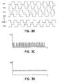
- Each stage of the series of stages in the upper charge pump line is similarly driven as successively delayed and inverted clock signals, as is illustrated in Figure 3B.
- the lower series of charge pump stages shown in Figure 3A are also driven by clock signals each delayed and inverted with respect to the clock signal driving the prior stage of the charge pump line.
- the first stage 320B 1 of the lower charge pump line is driven not by the clock signal CLK1 but rather by the delayed and inverted clock signal CLK2, so that whatever happens in the upper charge pump line will similarly happen in the lower charge pump line, though time delayed with respect thereto.
- each clock signal would drive n capacitors at a time.
- only two capacitors are driven at a time in the circuit of Figure 3A, the driving of all 2n capacitors being spread out over n time increments, wherein each time increment equals the delay of one of the delay circuits 330.
- the circuit of Figure 3A might, for instance, operate at the same clock frequency (preferably higher) as that of the prior art, the instantaneous loading on the power supply is greatly reduced and the frequency of the power supply current ripple is substantially increased, making the filtering of the ripple easier and more effective.
- the staggering and inverting of the drive of this stage also avoids the simultaneous replenishment of the charge of capacitors 322A 1 and 322B 1 in preparation for the next charge pumping operation. This, too, reduces the magnitude of the current spikes on the power supply.
- the inverting of the charge pump line starting signals also interleaves the output of the charge pump lines, reducing the output ripple voltage and increasing its frequency for easier filtering.
- Figure 4 illustrates one embodiment of the delay circuit 400 of the present invention.
- the delay circuit 400 includes P-channel MOS devices 404, 408, 410 and 416 and N-channel MOS devices 406, 412, 414 and 418.
- the delay circuit 400 receives an input clock signal CLKIN on an input signal line 402, delays the input clock signal CLKIN by a predetermined amount of time, and provides an inverted output clock signal CLKOUT on an output signal line 420. More specifically, when the input clock signal CLKIN goes low, N-channel device 406 turns off and P-channel device 404 turns on, causing node A to be pulled high to V dd .
- N-channel devices 408 and 410 Turn off and N-channel devices 412 and 414 turn on.
- N-channel device 412 turned on, node B is pulled down to V ss and causes N-channel device 418 to turn off.
- N-channel device 414 turned on, node C is also pulled down to the voltage at node B which is V ss . This causes P-channel device 416 to turn on. As such, the output clock signal CLKOUT is pulled high to V dd .
- N-channel device 414 assures that transistor 418 turns off before transistor 416 turns on, preventing both transistors from being on momentarily during the switching.
- N-channel device 404 turns off and N-channel device 406 turns on, causing node A to be pulled low to V ss .
- N-channel devices 412 and 414 are turned off and P-channel devices 408 and 410 are turned on.
- node B is first pulled high to V dd , thus causing P-channel device 416 to turn off.
- node B is pulled high to V dd , thereby causing N-channel device 418 to turn on.
- the output clock signal CLKOUT is pulled low to V ss .
- P-channel device 410 assures that transistor 416 turns off before transistor 418 turns on, again preventing both transistors from being on momentarily during the switching.
- the delay circuit 400 inverts and delays an input clock signal as stated.
- the delay circuits 330 1 -330 M are analog delay and inverting circuits, specifically successive inverter type circuits which merely impose a delay based upon the response time of the circuit.
- the clock signal CLK1 might be digitally generated, such as by way of example, dividing down a frequency n times the clock frequency CLK1, with each count of the higher frequency initiating the next successive delayed and inverted clock cycle.
- the M delayed and inverted clock signals may be equally staggered throughout the cycle time of one clock cycle CLK1 to maximize the smoothing effect of the present invention.
- the charge pump stage 320B 1 might be driven from the delayed clock signal CLK M/2 , with each subsequent stage being driven by the next subsequent delayed and inverted clock signal, using wrap-around to provide the full series of M delayed and inverted clock cycles.
- Such an embodiment would both equally stagger the replenishment of the charge on capacitors 322A1 and 322B 1 and equally stagger the pumping of the two charge pump lines to the output filter and load.
- the reduction in the power supply current spikes beyond that of the preferred embodiment disclosed would not be substantial.
- each clock signal generated by a delay circuit is inverted and delayed with respect to the input to the delay circuit.
- the total delay imposed by the combination of all delay circuits is at least one-half the period of clock signal CLK1 for best performance.
- the load on each clock driver i.e., delay circuit
- any switching current required by the delay circuits are spread out over time.
- the amplitude of the power supply current surges is small, and at a higher frequency, as shown in Figures 3C and 3D. This is to be distinguished from the prior art where large, lower frequency power supply current surges occur when the clock drivers are switching, and of course, the prior art clock drivers had to be large to drive the larger capacitive loads.
- the present invention provides a quieter system over the prior art, and alleviates the problem with the prior art of underprogramming or overprogramming a memory cell during the read-while-write programming method.
- the prior art charge pump circuit requires circuitry for ensuring that clocks CLK1 and CLK1B are non-overlapping as well as CLK2 and CLK2B, as opposed to the present invention where no such circuit is needed.
- the capacitors are made smaller and the clock frequency is increased, as the capacitance value of each capacitor is inversely proportional to the clock frequency for the same pumping capacity. This in turn requires still smaller delay clock drivers to drive the smaller capacitors.
- Increasing the clock frequency and decreasing the capacitor size increases the frequency of the output voltage ripple and decreases the amplitude of the output ripple, making the filtering of the charge pump output by resistor 342 and capacitor 344 easier and more effective.
- the current surges on the power supply are reduced and distributed due to smaller clock drivers and smaller loads.
- the overall size of the circuit is further reduced. This also reduces the output ripple, and provides for a quieter system and enhanced system performance.
Landscapes
- Engineering & Computer Science (AREA)
- Power Engineering (AREA)
- Dc-Dc Converters (AREA)
Applications Claiming Priority (2)
| Application Number | Priority Date | Filing Date | Title |
|---|---|---|---|
| US08/928,716 US6100752A (en) | 1997-09-12 | 1997-09-12 | Method and apparatus for reducing power supply current surges in a charge pump using a delayed clock line |
| US928716 | 2001-08-13 |
Publications (2)
| Publication Number | Publication Date |
|---|---|
| EP0902525A2 true EP0902525A2 (de) | 1999-03-17 |
| EP0902525A3 EP0902525A3 (de) | 1999-07-21 |
Family
ID=25456641
Family Applications (1)
| Application Number | Title | Priority Date | Filing Date |
|---|---|---|---|
| EP98307090A Withdrawn EP0902525A3 (de) | 1997-09-12 | 1998-09-03 | Verfahren und Vorrichtung zur Verminderung der Stromversorgungsstromspitzen in einer Ladungspumpe durch die Anwendung eines verzögerten Taktsignals |
Country Status (3)
| Country | Link |
|---|---|
| US (1) | US6100752A (de) |
| EP (1) | EP0902525A3 (de) |
| JP (1) | JPH11164545A (de) |
Cited By (7)
| Publication number | Priority date | Publication date | Assignee | Title |
|---|---|---|---|---|
| FR2800934A1 (fr) * | 1999-11-10 | 2001-05-11 | Mhs | Circuit elevateur de tension de type pompe de charge |
| US6370075B1 (en) | 1998-06-30 | 2002-04-09 | Sandisk Corporation | Charge pump circuit adjustable in response to an external voltage source |
| WO2002043232A3 (en) * | 2000-11-21 | 2003-01-03 | Mosaid Technologies Inc | Charge pump power supply |
| CN100568689C (zh) * | 2000-11-21 | 2009-12-09 | 睦塞德技术公司 | 电荷泵电源 |
| US7969235B2 (en) | 2008-06-09 | 2011-06-28 | Sandisk Corporation | Self-adaptive multi-stage charge pump |
| CN102290983A (zh) * | 2011-06-16 | 2011-12-21 | 北京大学 | 电荷泵 |
| TWI892421B (zh) * | 2023-02-02 | 2025-08-01 | 美商超捷公司 | 用於複數個電荷泵單元的泵送控制器 |
Families Citing this family (19)
| Publication number | Priority date | Publication date | Assignee | Title |
|---|---|---|---|---|
| JP2001078437A (ja) * | 1999-06-30 | 2001-03-23 | Toshiba Corp | ポンプ回路 |
| JP3476384B2 (ja) | 1999-07-08 | 2003-12-10 | Necマイクロシステム株式会社 | 昇圧回路とその制御方法 |
| JP3910765B2 (ja) * | 1999-09-08 | 2007-04-25 | 株式会社東芝 | 電圧発生回路及びこれを用いた電圧転送回路 |
| JP3614747B2 (ja) * | 2000-03-07 | 2005-01-26 | Necエレクトロニクス株式会社 | 昇圧回路、それを搭載したicカード及びそれを搭載した電子機器 |
| US6816000B2 (en) * | 2000-08-18 | 2004-11-09 | Texas Instruments Incorporated | Booster circuit |
| US6779122B2 (en) | 2000-12-26 | 2004-08-17 | Intel Corporation | Method and apparatus for executing a long latency instruction to delay the restarting of an instruction fetch unit |
| JP3871551B2 (ja) * | 2001-11-08 | 2007-01-24 | 日本テキサス・インスツルメンツ株式会社 | 電圧供給回路 |
| JP2003219633A (ja) * | 2002-01-17 | 2003-07-31 | Seiko Epson Corp | 昇圧回路 |
| KR100536603B1 (ko) * | 2003-07-10 | 2005-12-14 | 삼성전자주식회사 | 선택 모드를 갖는 전하 펌프 회로 |
| TWI233617B (en) * | 2004-01-02 | 2005-06-01 | Univ Nat Chiao Tung | Charge pump circuit suitable for low voltage process |
| US7457155B2 (en) * | 2006-08-31 | 2008-11-25 | Micron Technology, Inc. | Non-volatile memory device and method having bit-state assignments selected to minimize signal coupling |
| DE102009010550A1 (de) * | 2009-02-25 | 2010-09-02 | Texas Instruments Deutschland Gmbh | Ladungspumpe mit Selbsttaktung und Verfahren |
| EP2244365A1 (de) * | 2009-04-23 | 2010-10-27 | Mitsubishi Electric R&D Centre Europe B.V. | Verfahren und Vorrichtung zur Kondensatorentladung eines Boostwandlers, der sich aus mehreren Bridge-Geräten zusammensetzt |
| JP2011120407A (ja) * | 2009-12-04 | 2011-06-16 | Renesas Electronics Corp | チャージポンプ回路 |
| US9417685B2 (en) | 2013-01-07 | 2016-08-16 | Micron Technology, Inc. | Power management |
| US9491151B2 (en) | 2015-01-07 | 2016-11-08 | Ememory Technology Inc. | Memory apparatus, charge pump circuit and voltage pumping method thereof |
| US9300283B1 (en) * | 2015-02-18 | 2016-03-29 | Freescale Semiconductor,Inc. | Single capacitor, low leakage charge pump |
| WO2020206633A1 (en) * | 2019-04-10 | 2020-10-15 | Yangtze Memory Technologies Co., Ltd. | Reconfigurable voltage regulator |
| CN115622389A (zh) * | 2021-06-29 | 2023-01-17 | 合肥格易集成电路有限公司 | 电荷泵电路和存储器 |
Family Cites Families (9)
| Publication number | Priority date | Publication date | Assignee | Title |
|---|---|---|---|---|
| US3818309A (en) * | 1971-09-21 | 1974-06-18 | M Ichikawa | Dc transformer |
| NL8702734A (nl) * | 1987-11-17 | 1989-06-16 | Philips Nv | Spanningsvermenigvuldigschakeling en gelijkrichtelement. |
| JPH0817033B2 (ja) * | 1988-12-08 | 1996-02-21 | 三菱電機株式会社 | 基板バイアス電位発生回路 |
| US5036229A (en) * | 1989-07-18 | 1991-07-30 | Gazelle Microcircuits, Inc. | Low ripple bias voltage generator |
| DE4130191C2 (de) * | 1991-09-30 | 1993-10-21 | Samsung Electronics Co Ltd | Konstantspannungsgenerator für eine Halbleitereinrichtung mit kaskadierter Auflade- bzw. Entladeschaltung |
| US5191232A (en) * | 1992-03-17 | 1993-03-02 | Silicon Storage Technology, Inc. | High frequency voltage multiplier for an electrically erasable and programmable memory device |
| US5301097A (en) * | 1992-06-10 | 1994-04-05 | Intel Corporation | Multi-staged charge-pump with staggered clock phases for providing high current capability |
| US5629890A (en) * | 1994-09-14 | 1997-05-13 | Information Storage Devices, Inc. | Integrated circuit system for analog signal storing and recovery incorporating read while writing voltage program method |
| KR0167692B1 (ko) * | 1995-09-14 | 1999-02-01 | 김광호 | 반도체 메모리장치의 차아지 펌프회로 |
-
1997
- 1997-09-12 US US08/928,716 patent/US6100752A/en not_active Expired - Fee Related
-
1998
- 1998-09-03 EP EP98307090A patent/EP0902525A3/de not_active Withdrawn
- 1998-09-11 JP JP10258044A patent/JPH11164545A/ja active Pending
Cited By (11)
| Publication number | Priority date | Publication date | Assignee | Title |
|---|---|---|---|---|
| US6370075B1 (en) | 1998-06-30 | 2002-04-09 | Sandisk Corporation | Charge pump circuit adjustable in response to an external voltage source |
| US6556465B2 (en) | 1998-06-30 | 2003-04-29 | Sandisk Corporation | Adjustable circuits for analog or multi-level memory |
| US6760262B2 (en) | 1998-06-30 | 2004-07-06 | Sandisk Corporation | Charge pump circuit adjustable in response to an external voltage source |
| US7554844B2 (en) | 1998-06-30 | 2009-06-30 | Sandisk Corporation | Integrated circuit with analog or multilevel storage cells and user-selectable sampling frequency |
| FR2800934A1 (fr) * | 1999-11-10 | 2001-05-11 | Mhs | Circuit elevateur de tension de type pompe de charge |
| WO2002043232A3 (en) * | 2000-11-21 | 2003-01-03 | Mosaid Technologies Inc | Charge pump power supply |
| US6967523B2 (en) | 2000-11-21 | 2005-11-22 | Mosaid Technologies Incorporated | Cascaded charge pump power supply with different gate oxide thickness transistors |
| CN100568689C (zh) * | 2000-11-21 | 2009-12-09 | 睦塞德技术公司 | 电荷泵电源 |
| US7969235B2 (en) | 2008-06-09 | 2011-06-28 | Sandisk Corporation | Self-adaptive multi-stage charge pump |
| CN102290983A (zh) * | 2011-06-16 | 2011-12-21 | 北京大学 | 电荷泵 |
| TWI892421B (zh) * | 2023-02-02 | 2025-08-01 | 美商超捷公司 | 用於複數個電荷泵單元的泵送控制器 |
Also Published As
| Publication number | Publication date |
|---|---|
| JPH11164545A (ja) | 1999-06-18 |
| US6100752A (en) | 2000-08-08 |
| EP0902525A3 (de) | 1999-07-21 |
Similar Documents
| Publication | Publication Date | Title |
|---|---|---|
| US6100752A (en) | Method and apparatus for reducing power supply current surges in a charge pump using a delayed clock line | |
| US6359798B1 (en) | Charge pump voltage converter | |
| US6154088A (en) | Clocking scheme and charge transfer switch for increasing the efficiency of a charge pump or other circuit | |
| US5982222A (en) | High voltage generating circuit for a semiconductor memory device | |
| KR100696356B1 (ko) | 승압 회로 | |
| US7274248B2 (en) | Booster circuit and semiconductor device having same | |
| CA2428747C (en) | Charge pump power supply | |
| JP3422838B2 (ja) | 高電圧チャ−ジ・ポンプ | |
| US5790393A (en) | Voltage multiplier with adjustable output level | |
| WO2001024348A1 (en) | Method and apparatus for reducing stress across capacitors used in integrated circuits | |
| JP3323936B2 (ja) | 上昇率を制御するチャージ・ポンプ | |
| JPS63290159A (ja) | 昇圧回路 | |
| US20140111271A1 (en) | Semiconductor device having boosting circuit | |
| EP1559186A2 (de) | Variable ladungspumpenschaltung mit dynamischer last | |
| JPH06165482A (ja) | 電圧変換回路及びそれに用いる多相クロック発生回路 | |
| US6037622A (en) | Charge pump circuits for low supply voltages | |
| EP0404124B1 (de) | Eine Erhöhungsschaltung enthaltende Ladungspumpe, welche mit zwei Taktimpulssequenzen arbeitet | |
| JPH11110989A (ja) | 昇圧回路 | |
| JPS62502223A (ja) | 電圧マルチプライヤ回路 | |
| EP0433724A2 (de) | Spannungsregler mit Leistungszusatzsystem | |
| US6756837B2 (en) | Booster circuit | |
| US6838928B2 (en) | Boosting circuit configured with plurality of boosting circuit units in series | |
| US6831500B2 (en) | Noise-reduced voltage boosting circuit | |
| US5920225A (en) | Negative voltage drive circuit | |
| JP2004005773A (ja) | 昇圧装置 |
Legal Events
| Date | Code | Title | Description |
|---|---|---|---|
| PUAI | Public reference made under article 153(3) epc to a published international application that has entered the european phase |
Free format text: ORIGINAL CODE: 0009012 |
|
| AK | Designated contracting states |
Kind code of ref document: A2 Designated state(s): DE FR GB IT NL |
|
| AX | Request for extension of the european patent |
Free format text: AL;LT;LV;MK;RO;SI |
|
| PUAL | Search report despatched |
Free format text: ORIGINAL CODE: 0009013 |
|
| AK | Designated contracting states |
Kind code of ref document: A3 Designated state(s): AT BE CH CY DE DK ES FI FR GB GR IE IT LI LU MC NL PT SE |
|
| AX | Request for extension of the european patent |
Free format text: AL;LT;LV;MK;RO;SI |
|
| 17P | Request for examination filed |
Effective date: 19991213 |
|
| AKX | Designation fees paid |
Free format text: DE FR GB IT NL |
|
| STAA | Information on the status of an ep patent application or granted ep patent |
Free format text: STATUS: THE APPLICATION IS DEEMED TO BE WITHDRAWN |
|
| 18D | Application deemed to be withdrawn |
Effective date: 20030401 |