EP0896243A2 - Dispositif d'affichage réflectif à cristal liquide - Google Patents
Dispositif d'affichage réflectif à cristal liquide Download PDFInfo
- Publication number
- EP0896243A2 EP0896243A2 EP98114577A EP98114577A EP0896243A2 EP 0896243 A2 EP0896243 A2 EP 0896243A2 EP 98114577 A EP98114577 A EP 98114577A EP 98114577 A EP98114577 A EP 98114577A EP 0896243 A2 EP0896243 A2 EP 0896243A2
- Authority
- EP
- European Patent Office
- Prior art keywords
- liquid crystal
- display apparatus
- reflection type
- crystal display
- type liquid
- Prior art date
- Legal status (The legal status is an assumption and is not a legal conclusion. Google has not performed a legal analysis and makes no representation as to the accuracy of the status listed.)
- Withdrawn
Links
Images



Classifications
-
- G—PHYSICS
- G02—OPTICS
- G02F—OPTICAL DEVICES OR ARRANGEMENTS FOR THE CONTROL OF LIGHT BY MODIFICATION OF THE OPTICAL PROPERTIES OF THE MEDIA OF THE ELEMENTS INVOLVED THEREIN; NON-LINEAR OPTICS; FREQUENCY-CHANGING OF LIGHT; OPTICAL LOGIC ELEMENTS; OPTICAL ANALOGUE/DIGITAL CONVERTERS
- G02F1/00—Devices or arrangements for the control of the intensity, colour, phase, polarisation or direction of light arriving from an independent light source, e.g. switching, gating or modulating; Non-linear optics
- G02F1/01—Devices or arrangements for the control of the intensity, colour, phase, polarisation or direction of light arriving from an independent light source, e.g. switching, gating or modulating; Non-linear optics for the control of the intensity, phase, polarisation or colour
- G02F1/13—Devices or arrangements for the control of the intensity, colour, phase, polarisation or direction of light arriving from an independent light source, e.g. switching, gating or modulating; Non-linear optics for the control of the intensity, phase, polarisation or colour based on liquid crystals, e.g. single liquid crystal display cells
- G02F1/133—Constructional arrangements; Operation of liquid crystal cells; Circuit arrangements
- G02F1/1333—Constructional arrangements; Manufacturing methods
- G02F1/1335—Structural association of cells with optical devices, e.g. polarisers or reflectors
- G02F1/133553—Reflecting elements
-
- G—PHYSICS
- G02—OPTICS
- G02F—OPTICAL DEVICES OR ARRANGEMENTS FOR THE CONTROL OF LIGHT BY MODIFICATION OF THE OPTICAL PROPERTIES OF THE MEDIA OF THE ELEMENTS INVOLVED THEREIN; NON-LINEAR OPTICS; FREQUENCY-CHANGING OF LIGHT; OPTICAL LOGIC ELEMENTS; OPTICAL ANALOGUE/DIGITAL CONVERTERS
- G02F1/00—Devices or arrangements for the control of the intensity, colour, phase, polarisation or direction of light arriving from an independent light source, e.g. switching, gating or modulating; Non-linear optics
- G02F1/01—Devices or arrangements for the control of the intensity, colour, phase, polarisation or direction of light arriving from an independent light source, e.g. switching, gating or modulating; Non-linear optics for the control of the intensity, phase, polarisation or colour
- G02F1/13—Devices or arrangements for the control of the intensity, colour, phase, polarisation or direction of light arriving from an independent light source, e.g. switching, gating or modulating; Non-linear optics for the control of the intensity, phase, polarisation or colour based on liquid crystals, e.g. single liquid crystal display cells
- G02F1/133—Constructional arrangements; Operation of liquid crystal cells; Circuit arrangements
- G02F1/1333—Constructional arrangements; Manufacturing methods
- G02F1/1343—Electrodes
- G02F1/13439—Electrodes characterised by their electrical, optical, physical properties; materials therefor; method of making
-
- G—PHYSICS
- G02—OPTICS
- G02F—OPTICAL DEVICES OR ARRANGEMENTS FOR THE CONTROL OF LIGHT BY MODIFICATION OF THE OPTICAL PROPERTIES OF THE MEDIA OF THE ELEMENTS INVOLVED THEREIN; NON-LINEAR OPTICS; FREQUENCY-CHANGING OF LIGHT; OPTICAL LOGIC ELEMENTS; OPTICAL ANALOGUE/DIGITAL CONVERTERS
- G02F1/00—Devices or arrangements for the control of the intensity, colour, phase, polarisation or direction of light arriving from an independent light source, e.g. switching, gating or modulating; Non-linear optics
- G02F1/01—Devices or arrangements for the control of the intensity, colour, phase, polarisation or direction of light arriving from an independent light source, e.g. switching, gating or modulating; Non-linear optics for the control of the intensity, phase, polarisation or colour
- G02F1/13—Devices or arrangements for the control of the intensity, colour, phase, polarisation or direction of light arriving from an independent light source, e.g. switching, gating or modulating; Non-linear optics for the control of the intensity, phase, polarisation or colour based on liquid crystals, e.g. single liquid crystal display cells
- G02F1/133—Constructional arrangements; Operation of liquid crystal cells; Circuit arrangements
- G02F1/1333—Constructional arrangements; Manufacturing methods
- G02F1/1345—Conductors connecting electrodes to cell terminals
Definitions
- the present invention relates to a reflection type liquid crystal display apparatus provided with reflecting electrodes.
- a related art reflection type liquid crystal display apparatus is used in the TN or STN mode,
- the display apparatus is composed of a liquid crystal cell holding liquid crystal between two substrates on each of which transparent electrodes are formed; a pair of polarizing plates disposed so as to put this liquid crystal cell therebetween; and a reflecting plate disposed outside the polarizing plate of the lower substrate.
- a light passes through this pair of polarizing plates 4 times, so the display is dark.
- the transmittance of a light per polarizing plate is about 45% at highest. At this time, the transmittance of a polarized light in parallel to the absorbing axis of the polarizing plate is almost 0% and the transmittance of a vertically polarized light is almost 90%.
- the maximum reflectance will thus be about 33% even for a monochrome panel.
- the display will be darker than a monochrome panel, since the light is absorbed by the color filters. This is why it will become difficult to obtain a satisfactory brightness for a reflecting display.
- metallic reflecting electrodes are formed on the lower substrate so that each of them is used as both a reflecting plate and an electrode, and a reflecting plate is disposed in the liquid crystal cell. This is to solve a parallax problem caused by the thickness of the substrate provided between the reflecting plate and the liquid crystal.
- An Al or Ag metallic material which is low in wiring resistance and high in reflectance, is used for the metallic reflecting electrodes.
- the Ag material is expensive, but the Al material is used as a material of integrated circuits for general semiconductor devices (used to form elements on an Si wafer, for example). The Al material will thus be practical as a material of such the metallic reflecting electrodes.
- the stress migration problem means blistering (HIROKKU) of a thin film and wire breaking caused by a stress mainly in a heating process.
- the electro-migration means thin-film-like-wire breaking caused by electrical migration mainly at a power on operation (especially, a power-on operation under a high humidity and a high temperature).
- the reflection type liquid crystal display apparatus of the present invention comprises a liquid cell having an upper substrate having an electrode pattern formed with transparent electrodes, a lower substrate opposed to said upper substrate and having an electrode pattern formed with metallic reflecting electrodes, an orientation film formed on each of said two electrode patterns, and containing liquid crystal put between said upper and lower substrates, and an electronic part connected to said liquid crystal cell and used to drive said liquid crystal cell, wherein each of said metallic reflecting electrodes is a two-layer film composed of Ti and Al alloy and formed on said lower substrate.
- the resistance to each of stress migration, electro-migration, and corrosion can be improved significantly.
- low-price glass substrates can be employed for the display apparatus of the present invention.
- At least one of Zr, Ti, and Ta components should preferably be mixed by 0.1 at% to 5 at% in the Al alloy. If such a configuration is taken, the resistance to each of stress migration, electro-migration, and corrosion in the Al alloy material itself of the metallic reflecting electrodes will be improved more and it will be possible to provide excellent properties (low resistance of wiring, high reflectance of display electrodes) to the reflection type liquid crystal display apparatus.
- an exposed portion of electrode between an electrode to which the electronic part is connected and each display electrode is covered with resin.
- the resin covering the exposed portion should preferably be acrylic resign. Consequently, the resistance to each of electro-migration and corrosion will be improved more on the surface of each electrode at the exposed portion of metallic reflecting electrode and between electrode patterns in the reflection type liquid crystal display apparatus of the present invention.
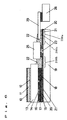
- Fig.1 is a cross sectional view of a reflection type liquid crystal display apparatus in the first embodiment of the present invention.
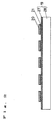
- Fig.2 illustrates how metallic reflecting electrodes are formed on the lower substrate in the first embodiment of the present invention.
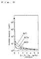
- Fig.3 illustrates the relationship among the Zr, Ti, and Ta contents and the HIROKKU density in the Al alloy film in the first embodiment of the present invention.
- Fig.4 illustrates the relationship among the Zr, Ti, and Ta contents and the reflectance in the Al alloy film in the first embodiment of the present invention.
- Fig.5 illustrates the relationship among the Zr, Ti, and Ta contents and the resistance in the Al alloy film in the first embodiment of the present invention.
- Fig.6 is a cross sectional view of the reflection type liquid crystal display apparatus in the second embodiment of the present invention.
- Fig.1 is a cross sectional view of the reflection type liquid crystal display apparatus in the first embodiment of the present invention.
- a reference numeral 10 indicates a polarizing plate, 11 indicates a polymer molecular film, 12 indicates a scattering film, and 13 indicates an upper substrate. 14 and 15 indicate orientation films. 16 indicates a transparent electrode, 17 indicates liquid crystal, 18 indicates a sealing member, and 19 indicates a lower substrate. 20 indicates an Al alloy electrode and 21 indicates a Ti electrode. 22 indicates acrylic resin and 23 indicates anisotropic binding material. 24 indicates a TAB tape carrier and 25 indicates an LSI chip. 26 indicates a printed board.
- Fig.2 is a cross sectional view indicating how Al alloy electrodes 20 and Ti electrodes 21 are formed on the lower substrate 19 shown in Fig.1.
- the electrodes 20 are metallic reflecting electrodes.
- 28 indicates a soda-lime glass substrate and 27 indicates an SiO 2 film. The reason why such an SiO 2 film is formed on the soda-lime glass substrate 28 is to prevent alkali from eluting into the liquid crystal.
- On this lower substrate 19 were laminated a Ti film 21 of 500 ⁇ and an Al alloy film 20 of 2000 ⁇ in order. Then, the same electrode patterns were formed by this two-layer film thereby to form two-layer film mirror reflection type metallic reflecting electrodes. On this lower substrate 19 was not formed any thin film active component such as a transistor.
- the upper substrate 13 was composed of a soda-lime glass substrate on which an SiO 2 film was formed. On the upper substrate 13 were formed transparent electrodes 16 with indium stannum oxide. No thin film active component such as a transistor was formed on this upper substrate 13.
- a 5wt% solution of polyimide N-methyl-2-pyrrolidinone was printed on both upper substrate 13 and lower substrate 19 on each of which electrodes were formed. Then, the surfaces of the substrates 13 and 19 were cured at 200°C and an orientating treatment was carried out to form orientation films 14 and 15 using rayon cloth under the control of the rotation rubbing method so as to materialize 250° twisted STN mode liquid crystal.
- thermal hardening sealing resin 18 mixed with 1.0wt% glass fiber of 5.5 ⁇ m in diameter was printed at the periphery on the upper substrate 13.
- On the lower substrate 19 was dispersed resin beads of 5.0 ⁇ m in diameter at a rate of 200 pieces/mm 2 .
- the upper and lower substrates 13 and 19 were put together and the sealing resin was cured at 150°C.
- liquid crystal obtained by mixing a predetermined amount of chiral liquid crystal with ester nematic liquid crystal of ⁇ n LC 0.16 was charged in vacuum between the substrates 13 and 19, then sealed with ultraviolet curing resin and cured with ultraviolet rays.
- a scattering film 12 was formed on the upper substrate 13 of the liquid crystal cell formed such way.
- the scattering film 12 was a forward scattering film (product name: Lumisty) manufactured by Sumitomo Kagaku Kogyo (Co., Ltd.) and the scattering angle of the scattering film was 0° to 50° when measured from the film normal.
- a polymer molecular film 11 composed of polycarbonate.
- the polymer molecular film 11 was composed of two polymer molecular films, each having a lag phase axis different from the other.
- the lag phase axis of the polymer molecular film at the liquid crystal cell side was 90° against the orientating direction of the upper substrate when the retardation was 0.3 ⁇ m and the lag axis of the upper polymer molecular film was 45° against the orientating direction of the upper substrate 13 when the retardation was 0.5 ⁇ m.
- an anti-glare (AG) neutral gray polarizing plate SQ-1852AP (Sumitomo Kagaku Kogyo Co., Ltd.) was stuck on the film as a polarizing plate 10 so that the absorbing axis was aligned to the lower lag axis.
- a parts-mounted printed board 26 and a TAB tape carrier 24 on which an LSI chip 25 is mounted were used as electronic parts for driving the liquid crystal cell and they were connected to each other.
- the electrodes 20 and 21 of the liquid crystal cell were extended thereby to compose an extended portion 100.
- the tip 100a of the extended portion 100 was then connected to one end of the TAB tape carrier using an anisotropic conductive binding material 23.
- part 100b of the extended portion 100 was covered with acrylic resin 22 so that the extended portion 100 of the electrodes 20 and 21 was not exposed.
- the portion 100b between the tip 100a of the extended portion 100 and a sealing member 18 was covered with acrylic resin 22 (TUFFY (TF1141) Hitachi Kasei Kogyo Co., Ltd.).
- This configuration has obtained a reflection type liquid crystal display apparatus in the normal back mode, which can display black as an achromatic color at a low reflectance, white as an achromatic color at a high reflectance, and vary the display from black to white as an achromatic color in the normally black mode respectively while the display is driven at a simple matrix of a 1/240 duty ratio.
- Tests were then performed as follows for such a reflection type liquid crystal display apparatus to check the resistance to stress migration, the resistance to electro-migration, the resistance to corrosion, the reflectance, and the specific resistance of the metallic reflecting electrodes when the content of each of Zr, Ti, and Ta (components of the Al alloy electrode 20) of the metallic reflecting electrodes was varied from 0at% to over 5at%.
- a sample of this test was formed by laminating a Ti film of 500 ⁇ and an Al alloy film of 2000 ⁇ on an SiO 2 -film-formed soda-lime glass substrate in order using the DC magnetron spattering method and using an Al alloy target in which the content of each of Zr, Ti, and Ta components was varied from 0at% to over 5at%, and a Ti target. Then, same pattern electrodes were formed in this two-layer film as two-layer mirror reflection metallic reflecting electrodes.
- a conducting test was carried out for the reflection type liquid crystal display apparatus composed shown in Fig.1 using the above metallic reflecting electrodes.
- the conducting test was continued for 500 hours at a temperature of 60°C and a humidity of 90%RH to evaluate the resistance to electro-migration of the electrodes.
- the content of each of Zr, Ti, and Ta in the alloy was 0at%, that is, when each electrode was a pure Al metallic reflecting electrode, wire breaking occurred.
- the content was between 0.1at% and over 5at%, no abnormality including wire breaking was recognized, even on the surface of the sample. This result thus proved that the resistance to electro-migration was improved when each of Zr, Ti, and Ta was added by 0.1at% or over.
- the test result has therefore proved that when the content of each of Zr, Ti, and Ta was between 0.1at% and over 5at% in the Al alloy of the metallic electrodes composed as described above, the resistance to stress migration, the resistance to electro-migration, and the resistance to corrosion were improved respectively.
- the present invention can thus provide a highly reliable reflection type liquid crystal display apparatus.
- the effect as described above can also be obtained even when the alloy contains two or more of Zr, Ti, and Ta components concurrently and the total amount of the contents is between 0.1at% and over 5at%.
- the Al alloy should preferably contain at least one of Zr. Ti, and Ta components by 0.1at% to 5at%.
- the alloy is composed so, it is possible to improve the resistance to stress migration, the resistance to electro-migration, and the resistance to corrosion of the Al alloy material itself, and accordingly, it is possible to obtain a reflection type liquid crystal display apparatus with low wiring resistance and high reflectance display electrodes.
- thin film active elements may be formed on the substrate by making (1) the display electrodes 20 and 21 on the lower substrate, (2) an electrode 100a for connecting an electronic part 25 used to drive the liquid crystal cell, and (3) an electrode 100b therebetween, of a two-layer film (Ti and Al alloy).
- a non-alkali glass substrate and a liquid crystal film substrate may be used instead of the glass substrate.
- the exposed portion of the electrode 100b between (1) the electrode 100a for connecting the electronic part used to drive the liquid crystal cell and (2) the display electrodes 20 and 21 is covered with acrylic resin 22 in the first embodiment, another resin such as silicon resin may be used to cover the portion.
- the resin should preferably be acrylic one that can prevent penetration of water so as to improve the resistance to electro-migration.
- scattering type electrodes may be employed as the metallic reflecting electrodes.
- the apparatus may be replaced with a color reflection type liquid crystal display apparatus.
- the liquid crystal may be replaced with another liquid crystal mode such as the TN mode, the PCGH mode, etc. thereby to compose the object reflection type liquid crystal display apparatus whose polarizing plate and polymer molecular film are adjusted to the liquid crystal mode.
- Fig.6 is a cross sectional view of the reflection type liquid crystal display apparatus in the second embodiment.
- the reflection type liquid crystal display apparatus in this second embodiment is composed almost in the same way as that in the first embodiment except that the COG method is used to mount the electronic part 25 used to drive the liquid crystal cell instead of the TAB method in the first embodiment.
- the electrodes 20 and 21 of the liquid crystal cell are connected to the LSI chip 25 using the anisotropic binding material 23.
- the electronic part (not illustrated) and the LSI chip 25 are used to drive the liquid crystal cell.
- the electrodes 200b and 200c formed between (1) the electrode 200a to which the flexible board 29 is connected and (2) the display electrodes are covered with acrylic resin 22 so as not to be exposed.
- the same effects can also be obtained in the metallic reflecting electrodes of the reflection type liquid crystal display apparatus composed in this second embodiment.
- the Al alloy should preferably contain at least one of Zr. Ti, and Ta components by 0.1at% to 5at%. When the alloy is composed so, it is possible to improve the resistance to stress migration, the resistance to electro-migration, and the resistance to corrosion of the Al alloy material itself, and accordingly, it is possible to obtain a reflection type liquid crystal display apparatus with low resistance wiring and high reflectance display electrodes.
- thin film active elements may be formed on the substrate if a two-layer film composed of Ti and Al alloy is used for (1) the display electrodes 20 and 21 on the lower substrate, (2) an electrode 200a for connecting an electronic part 29 used to drive the liquid crystal cell, and (3) electrodes 200b and 200c therebetween.
- a non-alkali glass substrate and a liquid crystal film substrate may be used instead of the glass substrate.
- the exposed portions of the electrodes 200b and 200c between (1) the electrode 200a for connecting the electronic part used to drive the liquid crystal cell and (2) the display electrodes 20 and 21 are covered with acrylic resin 22 in the the second embodiment, another resin such as silicon resin may be, used to cover the portions.
- the resin should preferably be acrylic one that can prevent penetration of water so as to improve the resistance to electro-migration.
- scattering type electrodes may be employed as the metallic reflecting electrodes.
- the apparatus may be replaced with a color reflection type liquid crystal display apparatus.
- the liquid crystal may be replaced with another liquid crystal mode such as the TN mode, the PCGH mode, etc. thereby to compose the object reflection type liquid crystal display apparatus whose polarizing plate and polymer molecular film are adjusted to the liquid crystal mode.
- the resistance to stress migration, the resistance to electro-migration, and the resistance to corrosion of the display apparatus can be improved significantly.
- the reflection type liquid crystal display apparatus can reduce the wiring resistance and increase the reflectance of the display electrodes.
- the reflection type liquid crystal display apparatus can improve the resistance to stress migration, the resistance to electro-migration, and the resistance to corrosion on the surface of the exposed portion of the metallic reflecting electrode, as well as between electrode patterns.
Landscapes
- Physics & Mathematics (AREA)
- Nonlinear Science (AREA)
- Mathematical Physics (AREA)
- Chemical & Material Sciences (AREA)
- Crystallography & Structural Chemistry (AREA)
- General Physics & Mathematics (AREA)
- Optics & Photonics (AREA)
- Liquid Crystal (AREA)
- Devices For Indicating Variable Information By Combining Individual Elements (AREA)
Applications Claiming Priority (3)
| Application Number | Priority Date | Filing Date | Title |
|---|---|---|---|
| JP20890297 | 1997-08-04 | ||
| JP20890297 | 1997-08-04 | ||
| JP208902/97 | 1997-08-04 |
Publications (2)
| Publication Number | Publication Date |
|---|---|
| EP0896243A2 true EP0896243A2 (fr) | 1999-02-10 |
| EP0896243A3 EP0896243A3 (fr) | 1999-09-08 |
Family
ID=16564026
Family Applications (1)
| Application Number | Title | Priority Date | Filing Date |
|---|---|---|---|
| EP98114577A Withdrawn EP0896243A3 (fr) | 1997-08-04 | 1998-08-03 | Dispositif d'affichage réflectif à cristal liquide |
Country Status (4)
| Country | Link |
|---|---|
| US (1) | US6011605A (fr) |
| EP (1) | EP0896243A3 (fr) |
| KR (1) | KR19990023344A (fr) |
| CN (1) | CN1209619A (fr) |
Cited By (2)
| Publication number | Priority date | Publication date | Assignee | Title |
|---|---|---|---|---|
| EP1116986A4 (fr) * | 1998-09-21 | 2001-11-07 | Matsushita Electric Industrial Co Ltd | Affichage reflectif a cristaux liquides |
| EP1111436A3 (fr) * | 1999-12-22 | 2002-10-23 | Matsushita Electric Industrial Co., Ltd. | Dispositif d'affichage à cristaux liquides du type réflectif |
Families Citing this family (13)
| Publication number | Priority date | Publication date | Assignee | Title |
|---|---|---|---|---|
| JP3339334B2 (ja) | 1996-12-05 | 2002-10-28 | 松下電器産業株式会社 | 反射型液晶表示素子 |
| TW482921B (en) * | 1997-06-16 | 2002-04-11 | Matsushita Electric Industrial Co Ltd | Reflective liquid crystal display device |
| JP3210274B2 (ja) | 1997-08-25 | 2001-09-17 | 松下電器産業株式会社 | 反射型液晶表示素子 |
| JP3670577B2 (ja) * | 2000-01-26 | 2005-07-13 | シャープ株式会社 | 液晶表示装置およびその製造方法 |
| KR100683648B1 (ko) * | 2000-04-26 | 2007-02-20 | 삼성에스디아이 주식회사 | 액정 디스플레이 모듈의 배선 실장방법 |
| JP4560924B2 (ja) * | 2000-09-19 | 2010-10-13 | ソニー株式会社 | 液晶表示装置 |
| US7019808B2 (en) * | 2000-09-21 | 2006-03-28 | Citizen Watch Co., Ltd. | Image device |
| JP2002328396A (ja) * | 2001-04-26 | 2002-11-15 | Nec Corp | 液晶表示装置及びその製造方法 |
| TWI312885B (en) * | 2001-12-06 | 2009-08-01 | Nec Lcd Technologies Ltd | Semi-transmissive liquid crystal display device |
| KR100916602B1 (ko) * | 2002-11-11 | 2009-09-11 | 엘지디스플레이 주식회사 | 소다라임 글라스를 이용한 액정표시장치와 그 제조방법 |
| JP4761425B2 (ja) * | 2004-05-12 | 2011-08-31 | 株式会社 日立ディスプレイズ | 表示装置および表示装置の製造方法 |
| US10356963B2 (en) | 2016-04-08 | 2019-07-16 | Shenzhen China Star Optoelectronics Technology Co., Ltd. | Ultrathin LCD module and liquid crystal display |
| CN105652520B (zh) * | 2016-04-08 | 2019-03-08 | 深圳市华星光电技术有限公司 | 一种超薄lcd模组及液晶显示器 |
Family Cites Families (16)
| Publication number | Priority date | Publication date | Assignee | Title |
|---|---|---|---|---|
| JPS5742022A (en) * | 1980-08-28 | 1982-03-09 | Toshiba Corp | Liquid crystal display device |
| JPS57113265A (en) * | 1980-12-29 | 1982-07-14 | Seiko Epson Corp | Semiconductor device and its manufacture |
| JP2610698B2 (ja) * | 1990-07-17 | 1997-05-14 | シャープ株式会社 | 反射型液晶表示装置の製造方法 |
| JP2722832B2 (ja) * | 1991-02-22 | 1998-03-09 | 日本電気株式会社 | 液晶表示素子 |
| JP2801487B2 (ja) * | 1992-04-30 | 1998-09-21 | シャープ株式会社 | パネルの実装構造および実装方法並びに樹脂供給硬化方法 |
| DE69321523T2 (de) * | 1992-06-26 | 1999-05-06 | Sharp K.K., Osaka | Reflektive Flüssigkristall-Anzeigevorrichtung |
| JP3080492B2 (ja) * | 1992-11-30 | 2000-08-28 | シャープ株式会社 | カラー液晶表示装置 |
| JP2812851B2 (ja) * | 1993-03-24 | 1998-10-22 | シャープ株式会社 | 反射型液晶表示装置 |
| EP0642050B1 (fr) * | 1993-09-02 | 2002-01-30 | Matsushita Electric Industrial Co., Ltd. | Modulateur spatial de lumière, procédé de fabrication et dispositif d'affichage par projection |
| JP3947575B2 (ja) * | 1994-06-10 | 2007-07-25 | Hoya株式会社 | 導電性酸化物およびそれを用いた電極 |
| US5822030A (en) * | 1994-09-16 | 1998-10-13 | Seiko Epson Corporation | Liquid crystal display device, its mounting structure and electronic device |
| EP0731507A1 (fr) * | 1995-03-08 | 1996-09-11 | International Business Machines Corporation | Matériaux d'électrodes |
| JP3349332B2 (ja) * | 1995-04-28 | 2002-11-25 | インターナショナル・ビジネス・マシーンズ・コーポレーション | 反射式空間光変調素子配列及びその形成方法 |
| JP3307181B2 (ja) * | 1995-07-31 | 2002-07-24 | ソニー株式会社 | 透過型表示装置 |
| KR0186206B1 (ko) * | 1995-11-21 | 1999-05-01 | 구자홍 | 액정표시소자 및 그의 제조방법 |
| KR100190041B1 (ko) * | 1995-12-28 | 1999-06-01 | 윤종용 | 액정표시장치의 제조방법 |
-
1998
- 1998-08-03 EP EP98114577A patent/EP0896243A3/fr not_active Withdrawn
- 1998-08-03 US US09/127,892 patent/US6011605A/en not_active Expired - Fee Related
- 1998-08-04 CN CN98116234A patent/CN1209619A/zh active Pending
- 1998-08-04 KR KR1019980031707A patent/KR19990023344A/ko not_active Withdrawn
Cited By (4)
| Publication number | Priority date | Publication date | Assignee | Title |
|---|---|---|---|---|
| EP1116986A4 (fr) * | 1998-09-21 | 2001-11-07 | Matsushita Electric Industrial Co Ltd | Affichage reflectif a cristaux liquides |
| US6608659B1 (en) | 1998-09-21 | 2003-08-19 | Matsushita Electric Industrial Co., Ltd. | Reflective liquid crystal display apparatus |
| EP1111436A3 (fr) * | 1999-12-22 | 2002-10-23 | Matsushita Electric Industrial Co., Ltd. | Dispositif d'affichage à cristaux liquides du type réflectif |
| US6597421B1 (en) | 1999-12-22 | 2003-07-22 | Matsushita Electric Industrial Co., Ltd. | Reflective liquid crystal display element and image display device using the same |
Also Published As
| Publication number | Publication date |
|---|---|
| CN1209619A (zh) | 1999-03-03 |
| KR19990023344A (ko) | 1999-03-25 |
| EP0896243A3 (fr) | 1999-09-08 |
| US6011605A (en) | 2000-01-04 |
Similar Documents
| Publication | Publication Date | Title |
|---|---|---|
| US6011605A (en) | Liquid crystal display with a metallic reflecting electrode having a two layer film of Ti and Al alloy | |
| US4466701A (en) | Highly reliable electrooptical device and process for manufacturing the same | |
| US6211931B1 (en) | Polymer-dispersed liquid crystal composition and liquid crystal display elements using the composition | |
| EP0327071B1 (fr) | Dispositif électro-optique | |
| EP1065554B1 (fr) | Affichage a cristaux liquides et sa fabrication | |
| KR19980063717A (ko) | 반사형 액정표시소자 | |
| WO2000051100A1 (fr) | Procede de montage d'un film sur un afficheur | |
| JP3304080B2 (ja) | 反射型液晶表示装置 | |
| JP3218222B2 (ja) | 反射型液晶表示装置 | |
| KR20010043956A (ko) | 반사형 액정 표시 장치 | |
| JP2001228464A (ja) | 液晶表示装置及び着色樹脂基板 | |
| JPH0736022A (ja) | 表示素子 | |
| JP3254421B2 (ja) | 液晶表示装置 | |
| JP3920417B2 (ja) | 液晶表示装置の製造方法 | |
| JP2876045B2 (ja) | カラー液晶表示素子とその製造方法及びカラー液晶表示装置 | |
| JP2000047165A (ja) | 反射型液晶表示装置の製造方法 | |
| JPH03167527A (ja) | カラー液晶表示素子及びカラー液晶表示装置 | |
| JPH06347812A (ja) | 液晶表示素子の電極間の短絡検査方法 | |
| JPH10170941A (ja) | 液晶表示装置 | |
| JP3709567B2 (ja) | 液晶表示モジュール | |
| JP2581074Y2 (ja) | 液晶表示装置 | |
| JP2023157680A (ja) | 液晶表示装置 | |
| JPH11281991A (ja) | 液晶表示装置 | |
| JPH11218776A (ja) | 液晶表示素子 | |
| EP1220013B1 (fr) | Elément optique à cristaux liquide et procédé de test de sa dureté de surface |
Legal Events
| Date | Code | Title | Description |
|---|---|---|---|
| PUAI | Public reference made under article 153(3) epc to a published international application that has entered the european phase |
Free format text: ORIGINAL CODE: 0009012 |
|
| AK | Designated contracting states |
Kind code of ref document: A2 Designated state(s): DE FR GB |
|
| AX | Request for extension of the european patent |
Free format text: AL;LT;LV;MK;RO;SI |
|
| PUAL | Search report despatched |
Free format text: ORIGINAL CODE: 0009013 |
|
| AK | Designated contracting states |
Kind code of ref document: A3 Designated state(s): AT BE CH CY DE DK ES FI FR GB GR IE IT LI LU MC NL PT SE |
|
| AX | Request for extension of the european patent |
Free format text: AL;LT;LV;MK;RO;SI |
|
| 17P | Request for examination filed |
Effective date: 19990928 |
|
| AKX | Designation fees paid |
Free format text: DE FR GB |
|
| STAA | Information on the status of an ep patent application or granted ep patent |
Free format text: STATUS: THE APPLICATION IS DEEMED TO BE WITHDRAWN |
|
| 18D | Application deemed to be withdrawn |
Effective date: 20040302 |