EP0890954B1 - Single-ended read, dual-ended write SRAM cell - Google Patents
Single-ended read, dual-ended write SRAM cell Download PDFInfo
- Publication number
- EP0890954B1 EP0890954B1 EP98104184A EP98104184A EP0890954B1 EP 0890954 B1 EP0890954 B1 EP 0890954B1 EP 98104184 A EP98104184 A EP 98104184A EP 98104184 A EP98104184 A EP 98104184A EP 0890954 B1 EP0890954 B1 EP 0890954B1
- Authority
- EP
- European Patent Office
- Prior art keywords
- bitline
- bitlines
- inverter
- write
- storage element
- Prior art date
- Legal status (The legal status is an assumption and is not a legal conclusion. Google has not performed a legal analysis and makes no representation as to the accuracy of the status listed.)
- Expired - Lifetime
Links
- 230000015654 memory Effects 0.000 claims description 35
- 230000008878 coupling Effects 0.000 claims 2
- 238000010168 coupling process Methods 0.000 claims 2
- 238000005859 coupling reaction Methods 0.000 claims 2
- 230000000295 complement effect Effects 0.000 claims 1
- 238000010586 diagram Methods 0.000 description 7
- 101100191136 Arabidopsis thaliana PCMP-A2 gene Proteins 0.000 description 3
- 101100048260 Saccharomyces cerevisiae (strain ATCC 204508 / S288c) UBX2 gene Proteins 0.000 description 3
- 230000003213 activating effect Effects 0.000 description 3
- 230000008901 benefit Effects 0.000 description 3
- 230000003068 static effect Effects 0.000 description 2
- 101100422768 Saccharomyces cerevisiae (strain ATCC 204508 / S288c) SUL2 gene Proteins 0.000 description 1
- 230000000903 blocking effect Effects 0.000 description 1
- 238000013500 data storage Methods 0.000 description 1
- 230000001934 delay Effects 0.000 description 1
- 230000003111 delayed effect Effects 0.000 description 1
- 238000001514 detection method Methods 0.000 description 1
- 230000009977 dual effect Effects 0.000 description 1
- 230000000694 effects Effects 0.000 description 1
- 238000011156 evaluation Methods 0.000 description 1
- 230000005669 field effect Effects 0.000 description 1
- 238000000034 method Methods 0.000 description 1
- 230000003014 reinforcing effect Effects 0.000 description 1
- 230000001960 triggered effect Effects 0.000 description 1
Images

Classifications
-
- G—PHYSICS
- G11—INFORMATION STORAGE
- G11C—STATIC STORES
- G11C8/00—Arrangements for selecting an address in a digital store
- G11C8/16—Multiple access memory array, e.g. addressing one storage element via at least two independent addressing line groups
-
- G—PHYSICS
- G11—INFORMATION STORAGE
- G11C—STATIC STORES
- G11C11/00—Digital stores characterised by the use of particular electric or magnetic storage elements; Storage elements therefor
- G11C11/21—Digital stores characterised by the use of particular electric or magnetic storage elements; Storage elements therefor using electric elements
- G11C11/34—Digital stores characterised by the use of particular electric or magnetic storage elements; Storage elements therefor using electric elements using semiconductor devices
- G11C11/40—Digital stores characterised by the use of particular electric or magnetic storage elements; Storage elements therefor using electric elements using semiconductor devices using transistors
- G11C11/41—Digital stores characterised by the use of particular electric or magnetic storage elements; Storage elements therefor using electric elements using semiconductor devices using transistors forming static cells with positive feedback, i.e. cells not needing refreshing or charge regeneration, e.g. bistable multivibrator or Schmitt trigger
- G11C11/412—Digital stores characterised by the use of particular electric or magnetic storage elements; Storage elements therefor using electric elements using semiconductor devices using transistors forming static cells with positive feedback, i.e. cells not needing refreshing or charge regeneration, e.g. bistable multivibrator or Schmitt trigger using field-effect transistors only
Definitions
- the present invention relates generally to the field of static random-access memory (SRAM), and more particularly to a system and method for constructing an SRAM cell with a fast, monotonic single-wire read path.
- SRAM static random-access memory
- SRAM cells are known in the art for storing a digital bit value and allowing that value to be written and read back. SRAM cells are used in many electronic applications requiring data storage, such as in the internal cache memory of a microprocessor.
- SRAM cells generally comprise one or more storage elements and circuitry to read and write digital bit values to the storage elements.
- the storage elements are connected to read and write circuitry by wires called bitlines.
- Storage elements indicate the stored bit value to the read circuitry by causing the voltage on the bitlines to change, or slew, from ground up to the supply voltage or from the supply voltage down to ground. A full voltage change is referred to as a rail-to-rail slew.
- the sense amp compares the two bitlines when it is triggered by a delayed clock line. This delay is calculated as the worst-case amount of time it takes for a storage element to cause the bitlines to slew apart enough for the sense amp to detect the difference. Unlike the storage element, the sense amp is large enough to quickly drive voltage changes, or state changes, to subsequent circuits.
- EP-A-0 473819 entitled “Multiport Memory Cell” and published 11.03.92, describes a memory cell connectable to two different bit lines under the selection of two independent word lines.
- the bit lines are connected to respective sense amplifiers.
- Each sense amplifier outputs the state of its respective bit line on the basis of comparing the change in potential on the respective bit line with a reference potential that is derived from the state of both bit lines.
- U.S. Patent 5,317,537, issued 31.05.94, entitled “Multi-Port Memory Device Having Precharged Bit Lines”, describes a multi-port memory cell array comprising a plurality of memory cells arranged in rows and columns. Each row of memory cells includes a corresponding dummy memory cell. The dummy cells are connected with associated ones of the word lines extending in the row direction. The dummy cells are further connected with dummy cell bit lines extending in the column direction.
- Sense amplifiers are connected to receive output bitlines of the memory cells and output bitlines of those dummy cells which are selected in a memory cell selection operation for amplifying differences between the selected memory cell outputs and the selected dummy cell outputs.
- sense amps imposes large size and component count burdens, both in the circuitry of the sense amp and in the delay circuitry.
- the minimum possible number of sense amps is used. This is done by placing as many storage elements as possible an one pair of bitlines with one sense amp. This has the undesirable side effect of loading down the bitlines, slowing voltage changes, forcing the worst-case delay of the sense amps to be drawn out even further. It also inhibits simultaneous reads of the storage elements which share one pair of bitlines.
- U.S. Patent 3,992,703, issued 16.11.76, entitled “Memory Output Circuit” describes a memory cell array comprising a plurality of memory cells arranged in rows and columns, with two bitlines per column. The configuration provides only a single read port per memory cell.
- EP-A-0473819 discloses a multi-port memory device having bitlines BLA and BLB, which are connected directly to sense amplifiers 10 and 12.
- the sense amplifiers 10 and 12 receive as input a respective bitline BLA and BLB and a reference voltage V REF determined from the values of bitlines BLA and BLB through transistors T7 and T8.
- U.S. 4,063,225 describes a memory cell array having first and second inverters coupled to form a flip-flop. Input signals are applied and information is read out from a single input/output point common to the output. Data is sensed by a sensing circuit that includes an inverter and a feedback transistor.
- U.S. 5,642,325 discloses a multi-port memory with a plurality of bit lines which are coupled to a static memory cell and independently controlled by select switches. Additional write transistors between the internal cell node and the common bit line node are foreseen for writing into the memory cell.
- a storage element may be physically connected to a sensor by wires and transistors, but no signal will pass from the storage element to the sensor because the transistor is turned off, blocking the electrical signal.
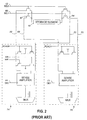
- the present invention may best be understood with reference to the prior art, as illustrated in FIG's 1-3.
- FIG. 1 illustrates a prior art SRAM cell.
- the supply voltage of the prior art SRAM cell is typically substantially greater than 2 volts, such as a 5 volt supply or a 3 volt supply.
- Storage element 10 has two input/output (I/O) port's 4, 6 which at any given time have values which are inverse to one another.
- Storage element 10 is generally as small and simple as possible to reduce the overall size of the memory circuitry.
- storage element 10 may comprise as few as four Field-Effect Transistors (FET's).
- FET's Field-Effect Transistors
- a select line 12 SELECT is connected to the gates of switch FET's 14 and 16. During a read or a write operation the select line 12 is activated, causing switch FET 16 to connect I/O port 6 of storage element 10 to bitline 26 and switch FET 14 to connect the inverse I/O port 4 of storage element 10 to bitline 20.
- Values are written to the storage element 10 by write lines 32 WR' and 34 WR which activate pulldown FET's 36 and 40, respectively. Either write line 32 or write line 34 is activated depending on what value is to be written.
- ground is shown as a triangle, as at 38.
- the supply voltage, Vdd is shown as a horizontal line making a 'T', as at 28.
- Prior art SRAM cells are often monotonic, in that the operation of the cells is divided into two clock states - a precharge state and an evaluate state.
- read and write operations occur only during the evaluation state.
- the bitlines are precharged to a logic high state to increase speed, since it can be faster to pull a line down to ground than to pull it up to Vdd.
- the precharge line 24 PCHG in FIG. 1 is activated and pullup FET's 26 and 30 connect bitlines 20 and 22 to Vdd to precharge them high.
- the evaluate state the precharge line 24 is deactivated, turning off pullup FET's 26 and 30.
- storage element 10 will only have to pull either bitline 20 or 22 to a logic low, leaving the other in its precharged logic high state.
- Values are read from the storage element 10 by disabling the precharge line 24 and activating select line 12 to connect the storage element 10 to bitlines 20 and 22.
- the prior art SRAM cell is a dual-ended read system, requiring examination of two bitlines to determine the value transmitted from the two inverse I/O port's 4 & 6 of storage element 10. As the storage element 10 is connected to the bitlines 20 and 22, one of the bitlines 20 or 22 will be pulled down toward ground while the other is left in its precharged high state, depending on the value of the stored bit.
- a sense amplifier 42 is used to detect differences of only several hundred millivolts between the two bitlines 20 and 22, resulting in a digital output on line 46.
- the bit value on the bitlines 20 and 22 can be read without waiting for one of the bitlines 20 or 22 to slew all the way from Vdd to ground.
- the sense amplifier 42 is activated by a clock line 44 CK which is hard-wired to delay a certain amount of time from the beginning of the read operation. This length of time is precalculated as the worst-case time it takes for bitlines 20 and 22 to slew down several hundred millivolts from the supply voltage, enabling the sense amplifier 42 to reliably detect the difference.
- the slew of several hundred millivolts that sense amplifier 42 requires to detect the difference is not reduced by a reduction of the supply voltage level. This minimum slew level is fixed by noise and transistor matching factors.
- the output line 46 of sense amplifier 42 is generally connected to a multiplexer 50 together with the output of other SRAM cells, allowing different memory locations to be read using address circuitry not shown, in configurations well-known to persons having ordinary skill in the art.
- the prior art SRAM cell is a single-port SRAM, allowing only one read operation at a time. SRAM cells are often extended to allow multiple read operations simultaneously.
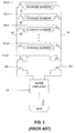
- FIG. 2 illustrates a prior art dual-port SRAM cell, which allows two simultaneous read operations.
- the addition of a second port requires the addition of second select line 60 SEL1 with switch FET's 62 and 64, two new bitlines 66 and 70, and a second group of read and precharge circuitry 76.
- the storage element 10 can thus be read by two different ports independently by activating select line 12 to read the stored bit value via circuitry group 74 or by activating select line 60 to read via circuitry group 76.
- storage element 10 may be required to pull bitlines 20 and 66 or 22 and 70 to ground at any given time. With two bitlines attached to each I/O port 4 or 6 of storage element 10 rather than one, the size of the wiring is increased, increasing the capacitance and requiring more power to drive a state change. Since the burden on storage element 10 is increased, voltage slews more slowly. Therefore, the hardwired worst-case delay of clock lines 44 and 72 must be made even longer.
- the number of sense amps is minimized as shown in FIG. 3 by connecting multiple storage elements 10, 80, 82 etc. to a single pair of bitlines 20 and 22 with their associated write, precharge, and sense amp circuitry.
- the use of double-ended bitlines with their associated sense amps is not ideal due to the size penalty. Minimizing this penalty by attaching many storage elements to each sense amp imposes speed penalties which somewhat offset the benefit of using sense amps. As each new storage element is added to a pair of bitlines, the capacitance of the system increases and voltage changes slow.
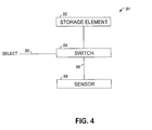
- FIG. 4 shows a SRAM cell 91.
- SRAM cell 91 has one storage element and a single port, comprising a storage element 92 switchably connected to a bitline 96 through a switch 94.
- the switch 94 is activated by a select line 90 SELECT.
- the stored value in the storage element 92 is determined by a sensor 98 based solely on the state of bitline 96.
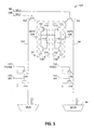
- FIG. 5 shows a monotonic, single-ended read, dual-ended write dual port SRAM cell 101 with one storage element.
- the supply voltage of this SRAM cell 101 is preferably less than approximately 2 volts.
- the phrase "logic high” indicates a voltage level substantially equal to the supply voltage Vdd and is interpreted as a value of 1.
- the phrase "logic low” indicates a voltage level substantially equal to ground, or 0 volts, and is interpreted as a value of 0.
- the storage element 92 is made up of four FET's 110, 112, 120, and 122 which form a pair of inverters 126 and 128.
- Inverters 126 and 128 operate to provide the logical inverse of their inputs 114 and 116 as follows. As the input 114 of the first inverter 126 becomes a logic high, pullup FET 110 turns off and pulldown FET 120 turns on, connecting the output 104 to ground and resulting in a logic low. As the input 114 becomes a logic low, pulldown FET 120 turns off and pullup FET 110 turns on, connecting the output 104 to the supply voltage (Vdd) resulting in a logic high.
- Output 106 is referred to as DATA and output 104 is referred to as DATA', where DATA' is the logical inverse of DATA.
- the pair of inverters 126 and 128 operate together in a loop to store the bit value.
- Output 104 of the first inverter 126 is connected to input 116 of the second inverter 128.
- Output 106 of the second inverter 128 is connected to input 114 of the first inverter 126.
- inverter 126 has a logic high on input 114
- a logic low results on output 104 of inverter 126 and input 116 of inverter 128.
- the logic low appears on input 116 of inverter 128, a logic high results on output 106, reinforcing the logic high which started the loop on input 114 of the first inverter 126.
- the bit value will be held in the loop.
- a select line 90 SEL0 operates switch FET 94 to electrically connect storage element 92 output 106 DATA to bitline 96 for read and write operations, and to disconnect storage element 92 from bitline 96 for precharge operations.
- a select line 100 SEL1 operates switch FET 102 to similarly electrically connect storage element 92 output 104 DATA' to bitline 124.
- the presently preferred SRAM cell shown in FIG. 5 is a monotonic system, divided into two clock states - a precharge state and an evaluate state.
- Precharge lines 130 PCHG0 and 132 PCHG1 are activated to connect bitlines 124 and 96 to Vdd through pullup FET's 134 and 136, respectively, during the precharge state. Read and write operations take place during the evaluate state.
- the SRAM cell of FIG. 5 is a dual-ended write system, using two bitlines. With the storage element 10 containing two inverters 126, 128 as described above, writing a new bit value can be accomplished by pulling down on the input of either inverter, depending on the value to be stored.
- precharge line 132 PCHG1 is disabled, then write line 142 WR is activated, connecting bitline 96 to ground through pulldown FET 146.
- Select line 90 SEL0 is also activated, connecting bitline 96 to input 114 of the first inverter 126 to change the value in the storage loop.
- pullup FET 112 of the second inverter 128 will still be on, attempting to hold input 114 of the first inverter 126 at a logic high state.
- pulldown FET's 144 and 146 are sized larger than pullup FET's 110 and 112 so that the pulldown FET's will overpower the pullup FET's during write operations.
- precharge line 130 PCHG0 is disabled, then write line 140 WR' is activated, connecting bitline 124 to ground through pulldown FET 144.
- Select line 100 SEL1 is also activated, connecting bitline 124 to input 116 of the second inverter 128 to change the value in the storage loop to a logic high.
- the SRAM cell of FIG. 5 is a single-ended read system, requiring only one bitline. Although two bitlines 124 and 96 are shown to enable writing a new value to storage element 10, writing could be accomplished in various other manners without the need for two bitlines, such as using the precharge pullup FET 136 to write a logic high value along with using pulldown FET 146 to write a logic low value.
- the circuit requires only a single bitline for a read operation. For example, to read the DATA value from storage element 10, select line 90 is activated, connecting output 106 to bitline 96 through switch FET 94.
- the supply voltage of storage element 10 is preferably substantially less than 2 volts, and bitline 96 is allowed to slew down from the supply voltage to a trip point of a standard component, such that a standard component such as an inverter or a multiplexer such as mux 98, shown in FIG. 5, may detect the bit value.
- the trip point of a typical component is about 60-70% of the supply voltage.
- the SRAM cell shown in FIG. 5 may be constructed with the following relative FET sizes: FET Size 94 3 102 3 110 1 112 1 120 5 122 5 134 3 136 3 144 3 146 3
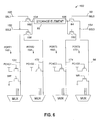
- Additional ports may be added as exemplified by the quad-port SRAM cell 150 of FIG. 6. Each new port requires the addition of a select line, switch FET, bitline and precharge circuit. Note that only two of the bitlines in this inventive example need write circuitry, one for each I/O port 104 & 106 of storage element 92.
- PORTO 170 and PORT1 162 may be identical to circuitry in SRAM cell 101 described in FIG. 5 above.
- An extra port PORT2 164 is shown, requiring select line SEL2 152, switch FET 156, bitline 172 and associated precharge circuitry. Bitline 172 does not require write circuitry, since write circuitry for I/O port 104 is included on bitline 124.
- An extra port PORT3 166 is also shown, requiring select line SEL3 154, switch FET 160, bitline 174 and associated precharge circuitry. Bitline 174 does not require write circuitry, since write circuitry for I/O port 106 is included on bitline 96.
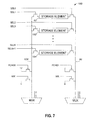
- FIG. 7 shows an SRAM cell 180 which may be identical to SRAM cell 101 described in FIG. 5 above except that it contains multiple storage elements 92, 182 and 184 connected to the pair of bitlines 124 and 96.
- the number of storage elements per pair of bitlines can be optimized for a desired balance of size versus speed for the overall memory circuitry. With sufficiently few storage elements per pair of bitlines, the present SRAM cell is faster and smaller than SRAM cells in the prior art.
Landscapes
- Engineering & Computer Science (AREA)
- Microelectronics & Electronic Packaging (AREA)
- Computer Hardware Design (AREA)
- Static Random-Access Memory (AREA)
Applications Claiming Priority (2)
| Application Number | Priority Date | Filing Date | Title |
|---|---|---|---|
| US891173 | 1997-07-10 | ||
| US08/891,173 US5815432A (en) | 1997-07-10 | 1997-07-10 | Single-ended read, dual-ended write SCRAM cell |
Publications (3)
| Publication Number | Publication Date |
|---|---|
| EP0890954A2 EP0890954A2 (en) | 1999-01-13 |
| EP0890954A3 EP0890954A3 (en) | 1999-06-16 |
| EP0890954B1 true EP0890954B1 (en) | 2006-08-02 |
Family
ID=25397742
Family Applications (1)
| Application Number | Title | Priority Date | Filing Date |
|---|---|---|---|
| EP98104184A Expired - Lifetime EP0890954B1 (en) | 1997-07-10 | 1998-03-09 | Single-ended read, dual-ended write SRAM cell |
Country Status (4)
| Country | Link |
|---|---|
| US (1) | US5815432A (enExample) |
| EP (1) | EP0890954B1 (enExample) |
| JP (1) | JPH1186561A (enExample) |
| DE (1) | DE69835399T2 (enExample) |
Families Citing this family (26)
| Publication number | Priority date | Publication date | Assignee | Title |
|---|---|---|---|---|
| US6046930A (en) * | 1998-09-01 | 2000-04-04 | International Business Machines Corporation | Memory array and method for writing data to memory |
| US6166946A (en) * | 2000-01-21 | 2000-12-26 | Hewlett-Packard Company | System and method for writing to and reading from a memory cell |
| JP2002056681A (ja) * | 2000-08-09 | 2002-02-22 | Toshiba Corp | メモリ装置 |
| US6560160B1 (en) | 2000-11-13 | 2003-05-06 | Agilent Technologies, Inc. | Multi-port memory that sequences port accesses |
| US6501688B2 (en) | 2001-05-30 | 2002-12-31 | Micron Technology, Inc. | tRCD margin |
| US6737685B2 (en) | 2002-01-11 | 2004-05-18 | International Business Machines Corporation | Compact SRAM cell layout for implementing one-port or two-port operation |
| JP3520283B2 (ja) | 2002-04-16 | 2004-04-19 | 沖電気工業株式会社 | 半導体記憶装置 |
| US20040013946A1 (en) | 2002-07-15 | 2004-01-22 | Ube Industries, Ltd. | Non-aqueous electrolytic solution and lithium battery |
| US7224024B2 (en) * | 2002-08-29 | 2007-05-29 | Micron Technology, Inc. | Single transistor vertical memory gain cell |
| US6838723B2 (en) * | 2002-08-29 | 2005-01-04 | Micron Technology, Inc. | Merged MOS-bipolar capacitor memory cell |
| US20040090820A1 (en) * | 2002-11-08 | 2004-05-13 | Saroj Pathak | Low standby power SRAM |
| US6804142B2 (en) * | 2002-11-12 | 2004-10-12 | Micron Technology, Inc. | 6F2 3-transistor DRAM gain cell |
| US7030436B2 (en) * | 2002-12-04 | 2006-04-18 | Micron Technology, Inc. | Embedded DRAM gain memory cell having MOS transistor body provided with a bi-polar transistor charge injecting means |
| JP4167127B2 (ja) | 2003-05-29 | 2008-10-15 | 沖電気工業株式会社 | 半導体集積装置 |
| JP4186768B2 (ja) * | 2003-09-16 | 2008-11-26 | 沖電気工業株式会社 | マルチポート半導体メモリ |
| US7403640B2 (en) * | 2003-10-27 | 2008-07-22 | Hewlett-Packard Development Company, L.P. | System and method for employing an object-oriented motion detector to capture images |
| US7242609B2 (en) * | 2005-09-01 | 2007-07-10 | Sony Computer Entertainment Inc. | Methods and apparatus for low power SRAM |
| US7545670B2 (en) * | 2007-07-10 | 2009-06-09 | Sony Computer Entertainment Inc. | Dual word line or floating bit line low power SRAM |
| US20130141997A1 (en) * | 2011-12-06 | 2013-06-06 | International Business Machines Corporation | Single-ended volatile memory access |
| US20130141992A1 (en) | 2011-12-06 | 2013-06-06 | International Business Machines Corporation | Volatile memory access via shared bitlines |
| US8817562B2 (en) * | 2012-07-31 | 2014-08-26 | Freescale Semiconductor, Inc. | Devices and methods for controlling memory cell pre-charge operations |
| US20140104960A1 (en) * | 2012-10-15 | 2014-04-17 | Sundar Iyer | Methods and Apparatus for Designing and Constructing High-Speed Memory Circuits |
| US9542995B2 (en) * | 2013-08-30 | 2017-01-10 | Manoj Sachdev | Threshold voltage mismatch compensation sense-amplifiers for static random access memories with multiple differential inputs |
| US11011222B2 (en) * | 2019-03-06 | 2021-05-18 | Arm Limited | Memory structure with bitline strapping |
| US11955169B2 (en) * | 2021-03-23 | 2024-04-09 | Qualcomm Incorporated | High-speed multi-port memory supporting collision |
| US11764764B1 (en) * | 2022-09-13 | 2023-09-19 | Nanya Technology Corporation | Latch device and operation method thereof |
Family Cites Families (6)
| Publication number | Priority date | Publication date | Assignee | Title |
|---|---|---|---|---|
| US3992703A (en) * | 1974-10-09 | 1976-11-16 | Rockwell International Corporation | Memory output circuit |
| US5034923A (en) * | 1987-09-10 | 1991-07-23 | Motorola, Inc. | Static RAM with soft defect detection |
| EP0473819A1 (en) * | 1990-09-05 | 1992-03-11 | International Business Machines Corporation | Multiport memory cell |
| JP3357382B2 (ja) * | 1991-05-28 | 2002-12-16 | 株式会社日立製作所 | 多ポートメモリ |
| US5642325A (en) * | 1995-09-27 | 1997-06-24 | Philips Electronics North America Corporation | Register file read/write cell |
| US5699292A (en) * | 1996-01-04 | 1997-12-16 | Micron Technology, Inc. | SRAM cell employing substantially vertically elongated pull-up resistors |
-
1997
- 1997-07-10 US US08/891,173 patent/US5815432A/en not_active Expired - Lifetime
-
1998
- 1998-03-09 DE DE69835399T patent/DE69835399T2/de not_active Expired - Lifetime
- 1998-03-09 EP EP98104184A patent/EP0890954B1/en not_active Expired - Lifetime
- 1998-07-10 JP JP10195181A patent/JPH1186561A/ja not_active Withdrawn
Also Published As
| Publication number | Publication date |
|---|---|
| DE69835399T2 (de) | 2007-01-04 |
| US5815432A (en) | 1998-09-29 |
| JPH1186561A (ja) | 1999-03-30 |
| EP0890954A2 (en) | 1999-01-13 |
| DE69835399D1 (de) | 2006-09-14 |
| EP0890954A3 (en) | 1999-06-16 |
Similar Documents
| Publication | Publication Date | Title |
|---|---|---|
| EP0890954B1 (en) | Single-ended read, dual-ended write SRAM cell | |
| US5325330A (en) | Memory circuit with foreshortened data output signal | |
| US5828610A (en) | Low power memory including selective precharge circuit | |
| US7643360B2 (en) | Method and apparatus for synchronization of row and column access operations | |
| US8208314B2 (en) | Sequential access memory elements | |
| US20040264279A1 (en) | High performance gain cell architecture | |
| US20010037429A1 (en) | Balanced switching method and circuit | |
| EP0591850B1 (en) | Semiconductor memory device | |
| US5563835A (en) | Sense amplification in data memories | |
| US6324110B1 (en) | High-speed read-write circuitry for semi-conductor memory | |
| US5400274A (en) | Memory having looped global data lines for propagation delay matching | |
| JPH03283184A (ja) | 半導体メモリ装置 | |
| US5835440A (en) | Memory device equilibration circuit and method | |
| EP1433179A1 (en) | System and method for early write to memory by holding bitline at fixed potential | |
| EP0547889B1 (en) | A tristatable driver for internal data bus lines | |
| US5801996A (en) | Data path for high speed high bandwidth DRAM | |
| KR100322541B1 (ko) | 입출력 라인쌍 등화회로 및 이를 구비한 메모리 장치 | |
| JPH04184785A (ja) | 半導体記憶装置 | |
| EP0547890A2 (en) | A read/write memory with interlocked write control | |
| US6909644B2 (en) | Semiconductor memory device | |
| JP2006527902A (ja) | メモリデータ線のための双方向バッファリング | |
| JP2003051189A (ja) | 小電圧信号の注入により、メモリへの早期書込みを行うシステム及び方法 | |
| EP0788107B1 (en) | Semiconductor memory device | |
| US5953739A (en) | Synchronous DRAM cache using write signal to determine single or burst write | |
| US5926426A (en) | Semiconductor memory device with single-cycle internal read/write function |
Legal Events
| Date | Code | Title | Description |
|---|---|---|---|
| PUAI | Public reference made under article 153(3) epc to a published international application that has entered the european phase |
Free format text: ORIGINAL CODE: 0009012 |
|
| AK | Designated contracting states |
Kind code of ref document: A2 Designated state(s): DE FR GB |
|
| AX | Request for extension of the european patent |
Free format text: AL;LT;LV;MK;RO;SI |
|
| PUAL | Search report despatched |
Free format text: ORIGINAL CODE: 0009013 |
|
| AK | Designated contracting states |
Kind code of ref document: A3 Designated state(s): AT BE CH DE DK ES FI FR GB GR IE IT LI LU MC NL PT SE |
|
| AX | Request for extension of the european patent |
Free format text: AL;LT;LV;MK;RO;SI |
|
| 17P | Request for examination filed |
Effective date: 19991126 |
|
| AKX | Designation fees paid |
Free format text: DE FR GB |
|
| RAP1 | Party data changed (applicant data changed or rights of an application transferred) |
Owner name: HEWLETT-PACKARD COMPANY, A DELAWARE CORPORATION |
|
| 17Q | First examination report despatched |
Effective date: 20020603 |
|
| GRAP | Despatch of communication of intention to grant a patent |
Free format text: ORIGINAL CODE: EPIDOSNIGR1 |
|
| GRAS | Grant fee paid |
Free format text: ORIGINAL CODE: EPIDOSNIGR3 |
|
| GRAA | (expected) grant |
Free format text: ORIGINAL CODE: 0009210 |
|
| AK | Designated contracting states |
Kind code of ref document: B1 Designated state(s): DE FR GB |
|
| REG | Reference to a national code |
Ref country code: GB Ref legal event code: FG4D |
|
| REF | Corresponds to: |
Ref document number: 69835399 Country of ref document: DE Date of ref document: 20060914 Kind code of ref document: P |
|
| ET | Fr: translation filed | ||
| PLBE | No opposition filed within time limit |
Free format text: ORIGINAL CODE: 0009261 |
|
| STAA | Information on the status of an ep patent application or granted ep patent |
Free format text: STATUS: NO OPPOSITION FILED WITHIN TIME LIMIT |
|
| 26N | No opposition filed |
Effective date: 20070503 |
|
| PGFP | Annual fee paid to national office [announced via postgrant information from national office to epo] |
Ref country code: GB Payment date: 20080327 Year of fee payment: 11 |
|
| PGFP | Annual fee paid to national office [announced via postgrant information from national office to epo] |
Ref country code: FR Payment date: 20080317 Year of fee payment: 11 |
|
| GBPC | Gb: european patent ceased through non-payment of renewal fee |
Effective date: 20090309 |
|
| REG | Reference to a national code |
Ref country code: FR Ref legal event code: ST Effective date: 20091130 |
|
| PG25 | Lapsed in a contracting state [announced via postgrant information from national office to epo] |
Ref country code: GB Free format text: LAPSE BECAUSE OF NON-PAYMENT OF DUE FEES Effective date: 20090309 Ref country code: FR Free format text: LAPSE BECAUSE OF NON-PAYMENT OF DUE FEES Effective date: 20091123 |
|
| PGFP | Annual fee paid to national office [announced via postgrant information from national office to epo] |
Ref country code: DE Payment date: 20100329 Year of fee payment: 13 |
|
| PG25 | Lapsed in a contracting state [announced via postgrant information from national office to epo] |
Ref country code: DE Free format text: LAPSE BECAUSE OF NON-PAYMENT OF DUE FEES Effective date: 20111001 |
|
| REG | Reference to a national code |
Ref country code: DE Ref legal event code: R119 Ref document number: 69835399 Country of ref document: DE Effective date: 20111001 |