EP0887763B1 - Verfahren und Vorrichtung zum Aufbau von Bitmap-Daten in einem Drucker - Google Patents
Verfahren und Vorrichtung zum Aufbau von Bitmap-Daten in einem Drucker Download PDFInfo
- Publication number
- EP0887763B1 EP0887763B1 EP98303714A EP98303714A EP0887763B1 EP 0887763 B1 EP0887763 B1 EP 0887763B1 EP 98303714 A EP98303714 A EP 98303714A EP 98303714 A EP98303714 A EP 98303714A EP 0887763 B1 EP0887763 B1 EP 0887763B1
- Authority
- EP
- European Patent Office
- Prior art keywords
- data
- blocks
- memory
- block
- block list
- Prior art date
- Legal status (The legal status is an assumption and is not a legal conclusion. Google has not performed a legal analysis and makes no representation as to the accuracy of the status listed.)
- Expired - Lifetime
Links
Images


Classifications
-
- G—PHYSICS
- G06—COMPUTING; CALCULATING OR COUNTING
- G06K—GRAPHICAL DATA READING; PRESENTATION OF DATA; RECORD CARRIERS; HANDLING RECORD CARRIERS
- G06K15/00—Arrangements for producing a permanent visual presentation of the output data, e.g. computer output printers
- G06K15/02—Arrangements for producing a permanent visual presentation of the output data, e.g. computer output printers using printers
-
- G—PHYSICS
- G06—COMPUTING; CALCULATING OR COUNTING
- G06K—GRAPHICAL DATA READING; PRESENTATION OF DATA; RECORD CARRIERS; HANDLING RECORD CARRIERS
- G06K2215/00—Arrangements for producing a permanent visual presentation of the output data
- G06K2215/0002—Handling the output data
- G06K2215/0062—Handling the output data combining generic and host data, e.g. filling a raster
- G06K2215/0065—Page or partial page composition
-
- G—PHYSICS
- G06—COMPUTING; CALCULATING OR COUNTING
- G06K—GRAPHICAL DATA READING; PRESENTATION OF DATA; RECORD CARRIERS; HANDLING RECORD CARRIERS
- G06K2215/00—Arrangements for producing a permanent visual presentation of the output data
- G06K2215/0002—Handling the output data
- G06K2215/0077—Raster outputting to the print element(s)
- G06K2215/008—Raster outputting to the print element(s) from more than one raster memory
Definitions
- the present invention relates generally to printing equipment and is particularly directed to a laser printer of the type which prints rasterized image data a single raster line at a time.
- the invention is specifically disclosed as a laser printer that forms blocks or tiles of bitmap image data and temporarily stores them in non-contiguous areas of dynamic random access memory, then retrieves a single raster line from each area as needed in real time to send the data in a serialized manner to the laser print engine.
- bitmap page image is divided up into a checkerboard pattern of units called "blocks."
- the number of blocks per page is dependent upon the paper size, block size, printhead resolution in dpi (dots per inch), and bitmap resolution in bits/pel.
- dpi dots per inch
- bitmap resolution bitmap resolution in bits/pel.
- an 8-1/2" x 11" page can be divided into rectangular blocks in which there are twenty (20) horizontal blocks x one hundred (100) vertical blocks on the page.
- each block would be 512 pels wide x 128 pels high.
- RAM random access memory
- memory is allocated on a block basis when information is "painted" into each block by the rasterization process. Therefore, each block of bitmap image data is stored in a separate area from the other similar blocks, and these smaller areas will quite likely to be spread all over different memory address locations of the printer's RAM.
- a transformation of the data stored in RAM must occur in conventional printers from a "scattered” block page representation to a "gathered” banded page representation, in which a "band” comprises a group of horizontal blocks that extend across the entire width of the printed page. This band building process copies the non-contiguous blocks into "band buffers" which each hold a page width strip in contiguous memory.
- multiple bands must be buffered before the image can be printed.
- a specific set of memory locations is reserved in the printer's main RAM system to hold these multiple bands.
- a minimum of two bands is typically stored in the system's RAM: (1) the band that is presently being sent to the laser printhead as a serial data stream, and (2) another band that is currently being built so that it will be completed (and ready to print) before the previous band has finished being printed.
- the band building process involves a copying operation of bitmap image data from the scattered blocks in non-contiguous RAM locations into the pre-allocated contiguous memory locations in RAM used to store the band buffer in real time (while the paper is moving through the printer), and thereby requiring a portion of the main processor's performance.
- null or "blank" blocks must be copied into the band buffer just like "real data” blocks, thereby requiring memory retrieval and storage operations that take up memory bandwidth (i.e., requiring access time to use the memory system's address and data busses).
- additional RAM locations must be allocated to hold the null block image data in the non-contiguous blocks, and additional memory must be allocated to hold the multiple band buffers.
- the blank physical patch is mapped back into the correct blank areas of the logical page image. This occurs during a serialization process, and if a particular mapped physical patch was found to be a zero patch, then the single blank physical patch in memory is accessed to ship the correct blank data (for the blank logical patch) to the printer.
- the non-blank data is mapped to physical memory addresses using logical patchified addresses, in which the physical addresses can be non-contiguous.
- the logical addresses which are contiguous use an offset (or pointer) to find the correct physical addresses to provide the proper data, as needed for the printer. This includes both blank and non-blank data as the individual patches of data are needed for the printer.
- United States Patent No. 5,502,804 discloses a laser printer that generates output page images in real time. Rather than requiring an entire page to be built in a bitmap form before sending it to the print engine, Butterfield discloses the use of building a single band to begin the process of printing, and after building the first band, a second band is created while the first band is being printed. By use of this method, a good deal of memory can be saved since an entire bitmap page need not be constructed before sending the data to a print engine. Even if sufficient memory is available to build a complete page, by using the banding technique of Butterfield a second page can be constructed in one band while a first page in another band is being printed.
- Butterfield receives high language level print job data and converts this data to "graphics orders" rather than converting directly to bitmaps. Since a single graphics command may affect more than one band, an order may be processed multiple times, using "command blocks” that are tabular structures in memory.
- An “order construction step” is first performed, and attempts to eliminate redundant orders by combining multiple inputs into single command blocks (thereby minimizing memory).
- a first (intermediate) image drawing step proceeds in parallel with the order construction step, and draws objects in the page image. The objects are stored in the user memory for use as source data for the next (or second) drawing step.
- the second (deferred) image drawing step begins when all of the orders for the page image have been generated. This step may process order commands multiple times, one for each image band affected.
- United States Patent No. 5,574,953 discloses a data compression and decompression system that stores compressed data in non-contiguous memory. As the data is compressed and stored in memory, the non-contiguous segments are marked, by placing a pointer at the last location that points to the next memory used. Just prior to the pointer, a special "link" code is stored, which logically links together the non-contiguous memory. When the data is decompressed, if the code is a link code, then the address pointer directs the system to the next location in memory where the next compressed data is stored to retrieve that segment. If the code is not a link code, then the code (or data) is decompressed.
- United States Patent No. 5,129,088 discloses a data processing system that creates virtual disks from non-contiguous groups of blocks on hard disk drives.
- Each drive (or drives) of physical memory locations is divided into physical partitions, each partition comprising a predetermined number of contiguous addressable blocks.
- the partitions in each group of blocks are not necessarily physically contiguous, although the "logical" blocks are contiguous.
- the system memory can automatically allocate one or more additional partitions, and this occurs dynamically to store further information.
- United States Patent No. 4,555,802 discloses a system that divides image data into a plurality of segments in which each segment is either square or rectangular. The segments are analyzed to determine which contain blank or zero data or which contain at least one bit of non-zero data. The blank segments are ignored and the non-blank segments are stored and indexed. A directory is created to indicate the storage location of each group of non-blank segments as well as their spatial location with respect to the rectangular raster array of signals. All compaction and decompaction machine operations are independent of bit-significant informational content of the segments.
- United States Patent No. 5,416,615 discloses a digital data transmitting device that extracts image data in both horizontal and vertical directions and forms an "original block" of n x n pixel data. From this information, a transformation operation is performed, such as a two-dimensional cosine transform, thereby creating a "differential block” that consists of m x m pixel data.
- the differential block data is "transform coded” to generate “coefficient data”, and a "flag generation circuit” is used to transmit the coefficient data.
- this flag generation circuit generates a flag if there is an omission of the transmission of coefficient data when there is no meaningful data (generally meaning blank data), and a separate transmission circuit will transmit the flag or flags and the pixel data of blocks.
- US 5,237,645 discloses a printing apparatus wherein empty blocks are not stored in an image memory, and effective blocks are stored in succession without leaving empty blocks therebetween.
- a "band" of rasterized bitmap image data must be constructed in contiguous memory before sending the band as serial data to the laser print engine.
- two separate bands have specific locations reserved in random access memory, one set of contiguous memory locations for the band that is now being output to the laser printhead, and a second set of contiguous memory locations for the band that is now being built.
- RAM random access memory
- a printing apparatus comprising:
- the invention also provides a method of efficiently storing bitmap print data and combining null and non-null bitmap print data for printing in real time in a printing system having a memory storage device, a print engine, said print engine containing a laser printhead, and a processing circuit, said method comprising the steps of:
- non-null data i.e., "real” data
- an improved printing apparatus receives a print job from a data source (such as a host computer), interprets that data, if necessary by rasterizing it into a bitmap, and then divides the bitmap image of a page to be printed, using a software page-map (PMAP) code, into a series of image blocks or tiles.
- the software uses a structure called the compressed page map (CPM) for all references to bitmap block, and the CPM contains a control header which describes characteristics of the page such as resolution, paper size, etc. After the control header, the CPM contains an entry for each block on the page.
- a data source such as a host computer
- Each entry of the CPM is a pointer to the block structure, which contains a control header that describes the characteristics of the block, such as block type, size, etc.
- the block structure contains the real block data, which is typically 8 KB in size.
- the printer software When starting a new page, the printer software references all blocks as null with no allocated memory in RAM. As the software paints black pels into the bitmap, blocks are first checked to see if they are null (all-white) or real (non-all-white). If the block to be painted into is null, the memory for the block must first be allocated (during this rendering or rasterizing procedure) before painting can proceed. If the block is real, it will have previously been allocated, and painting can proceed immediately.
- the printer software must serialize the data so as to convert it into a format understood by the laser printhead.
- the software builds a "block list table” (BLT) by processing entries from the CPM.
- the entries in the BLT are ordered from "entry 0" to "entry N” to correspond with the block order across the page. The ordering is from left to right on a simplex page and on the front side of a duplex page, and then from right to left on the back side of a duplex page.
- Each image block containing non-null data will be stored in the printer's memory system, although each block will likely be placed in a non-contiguous memory location with respect to other blocks on that particular page.
- the null image data blocks e.g., those image blocks containing only Logic 0 data in a printer which uses a print mechanism that develops a black pel with a Logic 1 bit from the bitmap
- Each entry in the block list table contains only the beginning address of the physical random access memory area that contains one of the image data blocks, but also contains other variables or attributes concerning the particular image data block, such as an expansion factor, whether this is the last block in the list for a "band" across the printed page, and whether or not this block is a regular non-null data block (i.e., a "real" data block), or a "no-op" (or "NOP") block containing null data.
- null data blocks require no physical memory address to be listed in their entry on the block list table, since no physical RAM areas are needed for storing null bitmap image data.
- the present invention Rather than building a band in contiguous memory before shipping rasterized data to the laser printhead, the present invention builds a series of rasterized line segments of bitmap data in real time and sends them to the laser printhead "on the fly,” by retrieving a single rasterized line segment of data, block-by-block, as needed to complete a single entire line required to define a "scan line" to be created on a photoconductive drum by a rotating polygonal mirror being struck by the laser's output beam.
- the preferred procedure for reading a single line from each block when needed is to access the block list table for a single band to be printed, place four (4) of the block list entries into a cache formed in the printer's ASIC, within which the individual block list entries are easily accessible by the Piecewise-Linear Direct Memory Access (PWLDMA) circuit from one block to the next within this cache.
- PWLDMA Piecewise-Linear Direct Memory Access
- a single band contains twenty (20) separate blocks across the horizontal width of the band, then to read a single raster line of the band would require five (5) separate transfers of groups of four (4) block list entries in and out of the cache. While a particular block list entry resides in the cache, at the appropriate time the block address is inspected to direct a read operation from the corresponding area of RAM that is holding the bitmap "real data" for this particular block. By use of pointers, the appropriate rasterized line segment of bitmap data will be read from the corresponding memory locations in RAM, and transferred into a first in first out (FIFO) memory in the ASIC (which essentially comprises a multi-entry register). As the laser printhead requires data for this particular line segment, the FIFO memory will provide serialized data at the appropriate data transmission rate.
- FIFO first in first out
- the printer's image system when its corresponding block list entry is inspected while residing in the cache, its "NOP" attribute will indicate that the printer's image system should not look to the RAM to find the "real data" for this particular block's rasterized line segment, but instead should pull a line segment of null data from a special NOP register residing within the ASIC.
- This NOP register will feed a line segment of either all zeros or ones (depending upon whether regular image data or reverse image data is desired for the printed page) to the FIFO memory in the ASIC.
- NOP register is a 32-bit general purpose register that will typically be filled with either all 1's or all 0's, however, it is not limited to this subset and its data set could contain other numeric values, including alternating 1's and 0's. Again at the appropriate time, this null data will be sent to the laser printhead at the appropriate data transmission rate from the bottom of the FIFO memory.
- One attribute stored in the ASIC for a particular print job is the width of the block to be printed, which depends upon the resolution (in bits/pel) and the width (in bits) of the physical block to be printed.
- This block width attribute will determine when the Piecewise-Linear DMA circuit should move to the next entry in the block list cache in order to build a particular band on the printed page.
- the "last block" of a band will not be required to be a “full” block, and only a "partial" block of data may be required to finish printing a particular line or band of the printed page.
- the present invention provides for both “full blocks” and “partial blocks”, and also allows the size of the band to be unbounded by allowing as many blocks as is necessary to build the band, with no artificial constraints being placed on the number of blocks for that band. Instead, the "last block” attribute in the block list entry tells the system when the last block has been arrived at while outputting data for a particular band.
- the data transfers out of RAM to load line segments of single raster lines from individual blocks into the FIFO memory are implemented using a piecewise-linear addressing mode direct memory access (DMA) procedure.
- DMA direct memory access
- the present invention merely reads the appropriate amount of data from a memory location holding the corresponding line segment data of a particular block from the RAM, and then directs that data into the FIFO memory. This saves memory bandwidth, thereby saving processing time for the processing system of the printer to perform other important tasks.
- Block List Table BLT
- BTC1 and BTC2 Block Transfer Count registers
- Block Width registers BW0 and BW1 Block Width registers
- the contiguous raster line is built from the non-contiguous blocks by manipulating the hardware registers in the ASIC, as follows:
- FIG. 1 shows a hardware block diagram of a laser printer generally designated by the reference numeral 10.
- Laser printer 10 will preferably contain certain relatively standard components, such as a DC power supply 12 which may have multiple outputs of different voltage levels, a microprocessor 14 having address lines, data lines, and control and/or interrupt lines, Read Only Memory (ROM) 16, and Random Access Memory (RAM), which is divided by software operations into several portions for performing several different functions.
- DC power supply 12 which may have multiple outputs of different voltage levels
- microprocessor 14 having address lines, data lines, and control and/or interrupt lines, Read Only Memory (ROM) 16, and Random Access Memory (RAM), which is divided by software operations into several portions for performing several different functions.
- ROM Read Only Memory
- RAM Random Access Memory
- Laser printer 10 also contains at least one serial input or parallel input port, or in many cases both types of input ports, as designated by the reference numeral 18 for the serial port and the reference numeral 20 for the parallel port. Each of these ports 18 and 20 would be connected to a corresponding input buffer, generally designated by the reference numeral 22 on Figure 1.
- Serial port 18 would typically be connected to a serial output port of a personal computer or a workstation that would contain a software program such as a word processor or a graphics package or computer aided drawing package.
- parallel port 20 could be connected to a parallel output port of the same type of personal computer or workstation containing the same types of programs.
- Such input devices are designated, respectively, by the reference numerals 24 and 26 on Figure 1.
- a common interpreter is PostScript , which is an industry standard used by most laser printers.
- PostScript is an industry standard used by most laser printers.
- the input data is typically sent to a common graphics engine to be rasterized, which typically occurs in a portion of RAM designated by the reference numeral 30 on Figure 1.
- a font pool and possibly also a font cache is stored, respectively, in ROM or RAM within most laser printers, and these font memories are designated by the reference numeral 32 on Figure 1.
- Such font pools and caches supply bitmap patterns for common alphanumeric characters so that the common graphics engine 30 can easily translate each such character into a bitmap using a minimal elapsed time.
- a queue manager or page buffer which is a portion of RAM designated by the reference numeral 34.
- an entire page of rasterized data is stored in the queue manager during the time interval that it takes to physically print the hard copy for that page, although the present invention treats this rasterized data in an entirely different manner than in previous printers.
- the data within the queue manager 34 is communicated in real time to a print engine designated by the reference numeral 36.
- Print engine 36 includes a laser light source within the printhead, and its output 46 is the physical inking onto a piece of paper, which is the final print output from laser printer 10.
- Print engine 36 contains an ASIC (Application Specific Integrated Circuit) 40, which acts as a controller and data manipulating device for the various hardware components within the print engine.
- ASIC Application Specific Integrated Circuit
- the bitmap print data arriving from Queue Manager 34 is received by ASIC 40, and at the proper moments is sent to the laser printhead.
- the address, data, and control lines are typically grouped in buses, which are electrically conductive pathways that are physically communicated in parallel (sometimes also multiplexed) around the various electronic components within laser printer 10.
- the address and data buses are typically sent to all ROM and RAM integrated circuits, and the control lines or interrupt lines are typically directed to all input or output integrated circuits that act as buffers.
- a set of buses at reference numeral 38 not only sends bitmap image data from queue manager 34 to print engine 36, but also sends addressing commands from ASIC 40 to queue manager 34, as will be described in greater detail hereinbelow.
- queue manager 34 of the present invention is not required to hold an entire page of image data before printing can be started by print engine 36.
- a bitmap image of a page to be printed is divided into rectangular "blocks" or "tiles”
- the actual bitmap data for each of these blocks or tiles is temporarily stored in a particular area of RAM, and these "areas” will also loosely be referred to herein as "blocks.”
- the separate areas or blocks of RAM will likely be non-contiguous, even when storing bitmap data for a single band to be printed, and a representation of these non-contiguous memory blocks is generally depicted by the reference numeral 50.
- a "block” list table 52 is also stored in dynamic RAM, and this block list table represents a descriptor table in which the various fields in the table describe attributes of the various blocks.
- One of these fields is an "address field" which points to the area of physical dynamic RAM that stores one of the bitmap image blocks. This will be described in greater detail hereinbelow.
- the ASIC 40 of print engine 36 contains several new components specifically used in connection with the present invention.
- a cache 60 is provided to hold several of the entries from the block list table 52.
- a pair of "Block List Address” registers 62 includes addressing information (i.e., pointers) for the physical memory address locations in dynamic RAM for two block list table 52.
- ASIC 40 also contains a special "no-op" register 64 that contains "null” data used when printing "empty" bitmap image blocks, or perhaps better described as when not “printing” such empty blocks, since typically no printed pels would be placed on paper for such empty areas on a physical sheet of paper. This no-op register 64 is also referred to herein as the "NOP" register.
- ASIC 40 also contains a first in, first out (FIFO) memory 66 which stores rasterized bitmap data for final output along a data path 42 to the laser printhead 44.
- FIFO first in, first out
- Figure 1 also diagrammatically depicts the fact that the main system address and data busses not only are used by microprocessor 14 and the various RAM components of the printer 10, but are also directed into ASIC 40 of the print engine 36.
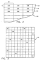
- Figure 2 depicts a portion of a page to be printed by printer 10, in which its upper left-hand corner portion is generally depicted by the reference numeral 100.
- Various rectangular blocks such as those indicated by reference numerals 102, 104, 106, 112, and 122 represent the so-called checkerboard pattern into which the bitmap image of the entire page is divided.
- the top row of blocks i.e., blocks 102, 104, 106, and 108) are the left-most blocks that comprise the top band that will later be printed line-by-line by the laser printhead of print engine 36.
- blocks 112, 114, 116, and 118 make up the left-most blocks of the second band from the top of the page
- blocks 122, 124, 126, and 128 make up the left-most blocks of the third band from the top of the page.
- each of these blocks contains 128 lines x 512 columns of pel or pixel data, at a bitmap resolution of one bit/pel, as represented by the dimensions "H" and "W” on Figure 2, respectively.
- the bitmap image data can be represented by an area in dynamic RAM of 8192 bytes (i.e., 8K, with each byte containing 8 bits), and each 8K area can be stored as a separate entity somewhere in the memory map of the printer's RAM.
- these memory areas will also be referred to herein as "blocks” and Figure 3 depicts such a memory map 50 that contains ten (10) such blocks, numbered blocks B0-B9.
- Each image block or tile, such as block 102, will generally contain one dot per pel.
- the image data could represent color data or Gray scale data, and for example, could require four (4) bits per pel, thereby requiring an area in memory of 32KB.
- a standard 8-1/2" x 11" page can be divided into a matrix of twenty (20) horizontal blocks x one hundred (100) vertical blocks, thereby requiring 2000 blocks per page.
- Each such block would require 8KB of RAM area to contain the pel data, and so it can be seen that a single band of bitmap image data would require twenty (20) such blocks, or 160KB of area in dynamic RAM of printer 10.
- each square of the memory map represents an 8KB area of RAM for printer 10, and the memory locations of adjacent squares would also have contiguous memory addresses in RAM. Since the blocks of image data can be broken down into 8KB divisions, it is not necessary for all of the blocks of a particular band to be located next to one another in a contiguous set of memory addresses. For example, on Figure 3, the first ten (10) blocks for a band are depicted by the descriptors B0-B9 and these are literally scattered all over the memory map 50.
- block B0 could represent the area required to store the bitmap image data for block 102 on Figure 2.
- block B1 could represent the area for storing the bitmap image data of block 104
- block B2 could represent the memory area required to store the bitmap image data for block 106.
- Figure 4 depicts a block list table generally designated by the reference numeral 52.
- this block list table 52 is a descriptor table which contains various fields of information at each entry in the table.
- the first entry designated by the reference numeral 150, includes various fields of information, such as two bits representing a "block expansion factor", i.e., a bit "BX1" at 152, and a bit "BX0" at 153.
- the expansion factor ratio is equal to 1:1, which is a replication of the original bitmap image data.
- the expansion factor ratio is 1:2, and two black pels are shipped out for every single Logic 1 data bit.
- expansion factors of 1:4 and 1:8 are also available in the preferred embodiment, in which either four (4) or eight (8) black pels are shipped out for every Logic 1 bitmap value.
- the reference numeral 154 represents the "address field" for the first entry 150 of the block list table 52.
- address field 154 represents the area of memory map 50 in which image bitmap data for the block B0 resides.
- Other fields in the block list table for the first entry 150 include an "LB" bit 156, and a "NOP" bit 158.
- this block list entry 150 does not represent the last block in the list for this particular band of bitmap image data.
- the last block in the band could be a partial block. This would be used in case the number of pels to be printed for a particular band is not precisely an exact multiple of the "Block Width," which is another parameter that is stored in the ASIC 40.
- the first block in the band can be a partial block. This will be discussed in greater detail below.
- the physical image data block for this block list entry was a null block (containing empty or zero data), and the system will call for a "no-op" transfer of data, which will be derived from a register within ASIC 40 rather than from a group of memory elements in the dynamic RAM of the printer's memory system.
- NOP 0
- the block list entry 160 includes an address pointer 164 for block B1, and has "Last Block” and “No-op” parameters specified at reference numerals 166 and 168, respectively.
- the third entry in the block list table at 170 similarly includes an address field 174 for block B2, and corresponding Last Block and No-op bits at 176 and 178, respectively.
- the bitmap image data may contain less than twenty bitmap image blocks containing any pel data that actually needs to be printed. In other words, some of the blocks within that band could be "empty" or zero data, in which no pels would be printed on the physical page at those actual block locations.
- the first band at the top of Figure 2 could contain twenty (20) total blocks of bitmap image data; however, only ten (10) of these blocks, for example, contain any "real" data that will actually be printed, and these are represented by the blocks designated B0-B9 on Figures 3 and 4.
- Figure 4 would contain a block list table in which the NOP bit is set to Logic 0 for all of the first ten (10) block list entries (i.e., those entries for blocks B0-B9). The next ten (10) block list entries would then contain a NOP value equal to Logic 1.
- the tenth block list entry at reference numeral 180 would contain a NOP equal to Logic 0 at numeral 188. If the entry 190 were one of the next ten (10) on this block list table, then the NOP at 198 would be set equal to Logic 1. Under these conditions, the address field 194 for block "BN" could be disregarded, or set to zero, since there is no physical area in dynamic RAM of printer 10 that contains the null data for this block. According to the present invention, null data blocks are not stored in memory, which saves a great deal of memory space when temporarily storing bitmap image data for a page to be printed. Later when it is time to print the band containing block BN, the appropriate null data will be sent to the print engine from a NOP register 64, as depicted on Figure 8. This will be described in greater detail hereinbelow.
- the block list table 52 on Figure 4 is conducive to piecewise-linear addressing, using a DMA (direct memory access) channel using a DMA controller 70 residing within ASIC 40.
- Each of the block list entries (such as entry 150) preferably are of a 32-bit width, or four bytes in size. When storing this information in the printer's dynamic RAM, it is preferred that contiguous physical memory locations be used to store these block list entries so that each block list entry can be accessed one after the other by merely shifting the address pointer by four bytes.
- a "Block List Address” parameter register generally designated by the reference numeral 62 on Figure 6, provides the address of the start of the block list table.
- the block list address for block B0 is located at reference numeral 250, and to address the next entry in the block list table as the DMA traverses blocks, the value ⁇ block number * 4 ⁇ is added to the block list address registers without updating the registers with the incremented value. This results in the identical list addressing for each pass through the list.
- the block list address registers are double buffered, and the block list table is also double buffered in data memory to support the DMA channels "autoreload" mode.
- This autoreload mode is clearly described hereinabove, and allows the various bands to be continually moved in and out of a first Block List Table 250 (i.e., BLA1) and a second Block List Table 252 (i.e., BLA2) while seamlessly continuing to copy raster line data into the FIFO 66.
- BLA1 Block List Table 1
- BLA2 Block List Table 2
- a cache designated by the reference numeral 60 on Figure 5 is created in memory elements of ASIC 40.
- Cache 60 can hold, in the preferred embodiment, four (4) block list entries at a given moment.
- the block list entry 150 could be placed. If that were to occur, then Cache #2 at 210 would contain the block list entry 160, Cache #3 at 220 would contain the block list entry 170, and Cache #4 at 230 would contain the block list entry for block B3.
- the address field 204 now located in Cache #1 would be the same as the address field 154.
- the bit expansion factors 202 and 203 would be the same as those bits 152 and 153, while the LB bit 206 would be the same as LB bit 156, and the NOP bit 208 would have the same value as the NOP bit 158.
- the address field in Cache #2-#4 are depicted by the reference numerals 214, 224, and 234, respectively. In this example, all four (4) block list entries currently residing in cache 60 contains "real data" and so the address fields 204, 214, 224, and 234 will point to actual physical memory locations in the dynamic RAM of printer 10.
- the Block List Address (BLA) registers 62 are preferably used to contain two (2) pointers to memory locations in the printer's dynamic RAM that hold the block list tables for data currently being processed.
- the BLA1 pointer at 250 will point to the memory element containing the first byte of a first block list table 54
- the BLA2 pointer 252 will point to a first byte of a second block list table (not shown).
- One of the important aspects of the present invention is its ability to quickly access the data required to build a single raster line of a band in real time and present this raster line to the print engine "on the fly" as paper is moving through the printer. This is accomplished by accessing the first four (4) block list entries by referring to the BLA register 62, and for this particular band this would be blocks B0-B3. As these four (4) block list entries are accessed from block list table 52, they are quickly placed into the cache 60 at the cache locations Cache #1-Cache #4. All four blocks relating to the entries 150, 160, 170, and 270 are quickly cycled through the two BLA registers, as described hereinabove.
- bitmap image data can be retrieved from the printer's dynamic RAM, block-by-block. block.
- this is under the control of DMA controller 70 that transfers the bitmap image data from dynamic RAM into a first in, first out (FIFO) memory 66 on Figure 7, which is also part of the ASIC 40.
- FIFO first in, first out
- the DMA controller 70 inspects the address field (i.e., field 204 in Cache #1 at 200) to find the beginning memory element that contains the bitmap data for block B0. After reading the number of data bits specified by the Block Width parameters BW1 and BW0, the appropriate amount of bitmap data is transferred into the first register at reference numeral 260 of the FIFO 66.
- Register #1 at numeral 260 contains only 512 bits of image data, which will eventually be transferred to the printhead of print engine 36 as a single raster line of serial information (which of course, is the desired result for a laser printer).
- DMA controller 70 will look to the address pointer of the address field 214 in Cache #2 at 210, which will point to the memory element location containing the "real data" for block B1.
- the DMA controller will now access the appropriate portions of this image data in the printer's dynamic RAM to extract only a single raster line of data from that block B1, and that single line segment is now placed into the FIFO 66.
- this raster line segment from block B1 will be placed at the top of FIFO 66, at register 260.
- the previous contents of register 260 will be shifted down into the next lower register 262, depicted as Register #2 in the FIFO.
- the raster line segment for block B0 is resident at register 266, and is available to be transferred along data path 42 to the laser printhead 44 at the appropriate data transmission rate for which that laser printhead desires to receive data.
- the data for the line segment of block B1 (temporarily residing in register 264) will then transfer down to the bottom register 266, and it too will become available to be transferred to the laser printhead 44.
- Another advantage of the present invention is the savings in memory bandwidth by using the cache 60 to hold the information for four (4) block list entries at a time.
- DMA controller 70 loads the cache 60 by transferring block list entries 150, 160, 170, and 270 into the cache locations 200, 210, 220, and 230, it requires four clock cycles to bring in the first block list entry.
- the printer can quickly increment through the cache to inspect the other block list entries. Since each such increment will require one clock cycle, it will require only seven (7) clock cycles to inspect all four block list entries within cache 60. Alternatively, if each block list entry was singularly referenced, a total of sixteen (16) clock cycles would be required. By this quick turnaround time of accessing through cache 60, the printer can very quickly bring in the appropriate raster line segment data for the four blocks presently about to be printed at the laser printhead 44.
- the block list entry will be loaded into the cache 60, as if it were any other block list entry containing real data.
- the system will realize that the DMA controller 70 need not go off and access any physical memory elements in the printer's dynamic RAM. Instead, the NOP register 64 (within ASIC 40) will be accessed to provide the appropriate 512-bit stream of raster line segment data. If in a "normal" print mode, then the NOP register 64 will provide 512 consecutive bits (i.e., assuming this is a "full block" defined by the BW0 register) having a Logic 0 value.
- NOP register 64 will provide 512 consecutive data bits having a Logic 1 value. This feature of the present invention not only saves physical RAM space by not storing null data blocks in the first place, but also unloads the memory and data busses of laser printer 10 and thereby increases its performance by not draining its memory bandwidth capacity.
- the Last Block (LB) attribute of the block list entry is used by cache 60 to inform the DMA controller 70 that it will soon be time to go to the next raster line of the block, or to go to an entire new block (for its first raster line) by bringing in four consecutive block entries for the appropriate image data block.
- the next block list entry to be accessed will cycle back to the first entry of the list, and this sequencing continues until the "transfer count” expires, which means the end of the band has been reached.
- the transfer count expires in autoreload mode
- the block list address and the transfer account are transferred from a "holding register" to the "active register” and the DMA channel is rearmed to continue processing DMA requests.
- an interrupt will trigger an interrupt service routine to rearm the channel.
- the last block in a band can be a "partial" block, which is required for bands having a data width that is not an exact multiple of the Block Width.
- the "BW0" parameter register is used for the block width for the first block through the next to last block in a band for pages being printed on their front side.
- the "BW1" parameter register is used for its block width.
- BW1 could have a value equal to BW0 for bands that are an exact multiple of a block width.
- the "BW1" parameter register is used for the block width for the first block in the band.
- the "BW0" parameter register is used for the block width.
Landscapes
- Engineering & Computer Science (AREA)
- General Engineering & Computer Science (AREA)
- Physics & Mathematics (AREA)
- General Physics & Mathematics (AREA)
- Theoretical Computer Science (AREA)
- Record Information Processing For Printing (AREA)
- Storing Facsimile Image Data (AREA)
Claims (14)
- Druckvorrichtung, umfassend:alle Blöcke, die Nicht-Null-Daten enthalten, in einer Bildtabelle des Hauptbereichs von Speicherelementen der Speicherschaltung temporär gespeichert sind und alle Blöcke, die Null-Daten enthalten, nicht in der Bildtabelle gespeichert sind; wobei die Vorrichtung dadurch gekennzeichnet ist, dass die Druckmaschine weiter einen Cache-Bereich von Speicherelementen (60), ein internes Register (64) und einen FIFO-Speicher (66) umfasst, wobei:(a) eine Speicherschaltung, wobei die Speicherschaltung einen Hauptbereich von Speicherelementen (34) enthält;(b) eine Druckmaschine (36) zum Empfang von Bitmapdruckdaten und zum Erstellen einer Ausgabe zu einem Druckmedium, wobei die Druckmaschine einen Laserdruckkopf (44) enthält; und(c) eine Verarbeitungsschaltung (14), die konfiguriert ist, um den Strom von Daten zwischen der Speicherschaltung und der Druckmaschine zu steuern und um Bitmapdruckdaten an die Druckmaschine abzugeben, wobei die Verarbeitungsschaltung auch konfiguriert ist, um die in der Speicherschaltung vorhandenen Bitmapdruckdaten von jeder durch die Druckmaschine zu druckenden Seite in eine Mehrzahl von Blöcken (50) von Bitmapdruckdaten einzuteilen, wobei eine Information über jeden der Mehrzahl von Blöcken einen entsprechenden Eintrag in einer Blocklistentabelle (52) aufweist; wobeiein Teil der Mehrzahl von Einträgen (150, 160...) der Blocklistentabelle im Cache temporär gespeichert ist und auf den, während er im Cache vorhanden ist, eingewirkt wird; undeine einzelne rästerisierte Zeile von Bitmapdruckdaten für jeden der Einträge über die Blöcke der momentan in dem Cache gespeicherten Blocklistentabelle aus der Bildtabelle für Blöcke, die Nicht-Null-Daten enthalten, wiedergewonnen wird und aus dem internen Register für Blöcke, die Null-Daten enthalten, wiedergewonnen wird, dann an den FIFO-Speicher übermittelt wird, und der FIFO die Bitmapdruckdaten ohne die Verwendung eines Bandpuffers zu den geeigneten Zeiten zu dem Druckkopf in Echtzeit überträgt.
- Druckvorrichtung nach Anspruch 1, bei der die Blöcke von Nicht-Null-Daten in der Bildtabelle an nichtbenachbarten körperlichen Speicherstellen gespeichert sind.
- Druckvorrichtung nach Anspruch 1 oder 2, bei der die Blocklistentabelle einen Pointer (164) einer Speicheradresse in der Bildtabelle für alle Blöcke speichert.
- Druckvorrichtung nach einem vorangehenden Anspruch, weiter umfassend eine Mehrzahl der Blocklistentabellen und mindestens ein Blocklistenadressregister (62), das einen Pointer zu Speicherelementen enthält, die mindestens eine von der Mehrzahl von Blocklistentabellen darstellen.
- Druckvorrichtung nach einem vorangehenden Anspruch, bei der das interne Register Daten für einen Null-Block enthält.
- Druckvorrichtung nach einem vorangehenden Anspruch, bei der die Bildtabelle Direktzugriffsspeicher enthält und das interne Register Speicherelemente einer in der Druckmaschine enthaltenen anwendungsspezifischen integrierten Schaltung (ASIC) (40) enthält.
- Druckvorrichtung nach einem vorangehenden Anspruch, bei der die Verarbeitungsschaltung konfiguriert ist, um auf die in dem Speicher vorhandenen Bitmapdruckdaten einzuwirken, um eine Mehrzahl von Bändern von Bitmapdruckdaten zu erzeugen, wobei jedes der Bänder eine Mehrzahl der Blöcke umfasst.
- Druckvorrichtung nach Anspruch 7, bei der die Verwendung des Cache und einer Blocklistentabelle ermöglicht, dass die Breite des Bandes unbegrenzt ist.
- Verfahren zum wirkungsvollen Speichern von Bitmapdruckdaten und Kombinieren von Null- und Nicht-Null-Bitmapdruckdaten zum Drucken in Echtzeit in einem Drucksystem mit einer Speicher-Speichereinrichtung, einer Druckmaschine (36), wobei die Druckmaschine einen Laserdruckkopf enthält, und einer Verarbeitungsschaltung (14), wobei das Verfahren die Schritte umfasst:(a) Einteilen von rasterisierten Bitmapdruckjobdaten von jeder durch die Druckmaschine zu druckenden Seite in eine Mehrzahl von Blöcken (50) von Bitmapdruckdaten, wobei jeder der Mehrzahl von Blöcken einen entsprechenden Eintrag in einer Blocklistentabelle (52) aufweist;(b) temporäres Speichern von allen Nicht-Null-Daten enthaltenden Blöcken in einer Bildtabelle eines Hauptbereichs von Speicherelementen (34) der Speicher-Speichereinrichtung, Nicht-Speichern von allen Blöcken, die Null-Daten enthalten, in der Bildtabelle und temporäres Speichern von Information über jeden der Nicht-Null-Daten-Blöcke in einem Eintrag in der Blocklistentabelle;(c) temporäres Speichern von Information über jeden der Null-Daten-Blöcke in einem Eintrag in der Blocklistentabelle; wobei das Verfahren dadurch gekennzeichnet ist, dass die Druckmaschine weiter einen Cache-Bereich von Speicherelementen (60), ein internes Register (64) und einen FIFO-Speicher (66) umfasst; wobei das Verfahren weiter durch die Schritte gekennzeichnet ist:(d) temporäres Speichern eines Teils der Mehrzahl von Einträgen der Blocklistentabelle in dem Cache;(e) Wiedergewinnen einer einzelnen rasterisierten Zeile von Bitmapdruckdaten für jeden der Einträge über die Blöcke der momentan in dem Cache gespeicherten Blocklistentabelle aus der Bildtabelle für Blöcke, die Nicht-Null-Daten enthalten, und aus dem internen Register für Blöcke, die Null-Daten enthalten;(f) Übermitteln der einzelnen rasterisierten Zeile von jedem der Einträge über die Blöcke der momentan in dem Cache gespeicherten Blocklistentabelle an einen FIFO-Speicher; und(g) Übertragen, der Bitmapdruckdaten von dem FIFO zu der Druckmaschine zu geeigneten Zeiten in Echtzeit ohne Bandpuffern.
- Verfahren nach Anspruch 9, bei dem die Blöcke von Nicht-Null-Daten in der Bildtabelle an nichtbenachbarten körperlichen Speicherstellen gespeichert werden.
- Verfahren nach Anspruch 9 oder 10, weiter umfassend den Schritt: Speichern eines Pointers (164) einer Speicheradresse in der Bildtabelle für alle Blöcke in der Blocklistentabelle.
- Verfahren nach einem der Ansprüche 9 bis 11, weiter umfassend: Bereitstellen einer Mehrzahl von Blocklistentabellen und mindestens eines Blocklistenadressregisters (62), das einen Pointer zu Speicherelementen enthält, die mindestens eine von der Mehrzahl von Blocklistentabellen darstellen.
- Verfahren nach einem der Ansprüche 9 bis 12, bei dem das interne Register Daten für einen Null-Block enthält.
- Verfahren nach einem der Ansprüche 9 bis 13, bei dem die Bildtabelle Direktzugriffsspeicher enthält und das interne Register Speicherelemente einer in der Druckmaschine enthaltenen anwendungsspezifischen integrierten Schaltung (ASIC) (40) enthält.
Applications Claiming Priority (2)
| Application Number | Priority Date | Filing Date | Title |
|---|---|---|---|
| US854607 | 1997-05-12 | ||
| US08/854,607 US5870535A (en) | 1997-05-12 | 1997-05-12 | Method and apparatus for building rasterized lines of bitmap data to be printed using a piecewise-linear direct memory access addressing mode of retrieving bitmap data line segments |
Publications (3)
| Publication Number | Publication Date |
|---|---|
| EP0887763A2 EP0887763A2 (de) | 1998-12-30 |
| EP0887763A3 EP0887763A3 (de) | 2001-04-11 |
| EP0887763B1 true EP0887763B1 (de) | 2005-10-12 |
Family
ID=25319148
Family Applications (1)
| Application Number | Title | Priority Date | Filing Date |
|---|---|---|---|
| EP98303714A Expired - Lifetime EP0887763B1 (de) | 1997-05-12 | 1998-05-12 | Verfahren und Vorrichtung zum Aufbau von Bitmap-Daten in einem Drucker |
Country Status (7)
| Country | Link |
|---|---|
| US (1) | US5870535A (de) |
| EP (1) | EP0887763B1 (de) |
| JP (1) | JPH1191173A (de) |
| KR (1) | KR100597879B1 (de) |
| CN (1) | CN1129061C (de) |
| DE (1) | DE69831835T2 (de) |
| TW (1) | TW424201B (de) |
Families Citing this family (46)
| Publication number | Priority date | Publication date | Assignee | Title |
|---|---|---|---|---|
| JPH0971013A (ja) * | 1995-05-10 | 1997-03-18 | Canon Inc | 印刷制御装置及びメモリ制御方法及び印刷制御方法及び制御プログラムを記憶した記憶媒体 |
| US6115134A (en) * | 1997-12-05 | 2000-09-05 | Hewlett-Packard Company | Scan line splitting in a multi-staged image processing pipeline |
| US6195473B1 (en) * | 1997-12-26 | 2001-02-27 | International Business Machines Corporation | Non-integer scaling of raster images with image quality enhancement |
| US6226420B1 (en) * | 1997-12-26 | 2001-05-01 | International Business Machines Corporation | Non-integer scaling of raster images |
| US6181835B1 (en) * | 1997-12-26 | 2001-01-30 | International Business Machines Corporation | Non-integer scaling of raster images with image quality enhancement using an anamorphically scaled intermediate bitmap |
| JPH11348358A (ja) * | 1998-06-09 | 1999-12-21 | Ricoh Co Ltd | 画像形成装置 |
| US6502181B1 (en) | 1999-09-17 | 2002-12-31 | Zilog, Inc. | Method and apparatus for an enhanced processor |
| FR2801396B1 (fr) | 1999-11-22 | 2002-11-08 | Canon Kk | Convertion en mode point de donnees numeriques |
| JP2001158146A (ja) * | 1999-12-03 | 2001-06-12 | Fujitsu Ltd | 印字制御装置 |
| US6238037B1 (en) | 2000-02-07 | 2001-05-29 | Lexmark International, Inc. | Method of multi-dot interlace printing |
| US6651116B1 (en) * | 2000-05-15 | 2003-11-18 | International Business Machines Corporation | Output interface for a raster object memory in a method, system and program |
| US6557135B1 (en) * | 2000-05-17 | 2003-04-29 | Lucent Technologies Inc. | Cycling through entirety of error-indicating acknowledgment information |
| US8270023B2 (en) * | 2000-05-23 | 2012-09-18 | Zamtec Limited | Print engine controller for double-buffered processing |
| AU770625B2 (en) * | 2000-12-28 | 2004-02-26 | Canon Kabushiki Kaisha | Pipelining of rendered data with variable sized buffers |
| US6697881B2 (en) * | 2001-05-29 | 2004-02-24 | Hewlett-Packard Development Company, L.P. | Method and system for efficient format, read, write, and initial copy processing involving sparse logical units |
| US7324229B2 (en) * | 2002-04-10 | 2008-01-29 | Texas Instruments Incorporated | Rendering in a printer using bands |
| JP4018433B2 (ja) | 2002-04-15 | 2007-12-05 | キヤノン株式会社 | 記録装置 |
| JP4401618B2 (ja) * | 2002-04-15 | 2010-01-20 | キヤノン株式会社 | 記録装置、及び、バッファ管理方法 |
| JP4371632B2 (ja) * | 2002-06-05 | 2009-11-25 | キヤノン株式会社 | 画像記録装置及びその記録制御方法 |
| JP4510395B2 (ja) * | 2003-03-27 | 2010-07-21 | キヤノン株式会社 | 記録装置 |
| US7710602B2 (en) * | 2003-03-31 | 2010-05-04 | Sharp Laboratories Of America, Inc. | Systems and methods for context-based adaptive image processing using segmentation |
| US7359082B2 (en) * | 2003-10-20 | 2008-04-15 | Marvell International Technology Ltd. | Independent video hardware blocks to support laser printers |
| CN1299196C (zh) * | 2004-02-23 | 2007-02-07 | 致伸科技股份有限公司 | 动态调整打印作业的系统及其方法 |
| CN100351856C (zh) * | 2004-06-04 | 2007-11-28 | 北京北大方正电子有限公司 | 一种能够减少页面预光栅化时间的打印控制方法 |
| US7684076B2 (en) * | 2004-07-23 | 2010-03-23 | Kabushiki Kaisha Toshiba | Method and apparatus for raster image processing |
| JP4272603B2 (ja) * | 2004-08-20 | 2009-06-03 | 株式会社沖データ | 情報処理装置 |
| CN100361067C (zh) * | 2004-12-31 | 2008-01-09 | 东友科技股份有限公司 | 打印文件的分页方法 |
| CN100351857C (zh) * | 2005-01-07 | 2007-11-28 | 北京北大方正电子有限公司 | 一种能够减少打印内存需求的打印控制方法 |
| JP4603933B2 (ja) | 2005-05-23 | 2010-12-22 | キヤノン株式会社 | 記録装置 |
| CN100356395C (zh) * | 2005-06-13 | 2007-12-19 | 北京北大方正电子有限公司 | 一种能够避免打印越界错误的打印控制方法 |
| KR100759906B1 (ko) * | 2005-09-30 | 2007-09-18 | 삼성전자주식회사 | 주소록의 선택적 인쇄 기능을 갖는 화상형성장치 및 인쇄시스템 그리고 그들의 인쇄방법 |
| JP4659581B2 (ja) * | 2005-10-07 | 2011-03-30 | キヤノン株式会社 | 画像処理装置及びその制御方法、プログラム |
| US8488133B2 (en) * | 2006-08-30 | 2013-07-16 | Lexmark International, Inc. | System and method for marking print media |
| JP4881140B2 (ja) * | 2006-12-07 | 2012-02-22 | キヤノン株式会社 | データ転送装置、データ転送制御方法、およびデータ転送制御プログラム |
| US8472066B1 (en) | 2007-01-11 | 2013-06-25 | Marvell International Ltd. | Usage maps in image deposition devices |
| CN101178775B (zh) * | 2007-12-11 | 2010-04-14 | 北大方正集团有限公司 | 二值图打印数据的处理方法 |
| DE102008052421A1 (de) * | 2008-10-21 | 2010-04-22 | Giesecke & Devrient Gmbh | Vorrichtung und Verfahren zum Bedrucken eines Banderolenstreifens |
| JP5268617B2 (ja) * | 2008-12-17 | 2013-08-21 | キヤノン株式会社 | 画像形成装置、画像形成装置の制御方法及びコンピュータプログラム |
| US8243313B2 (en) * | 2009-05-26 | 2012-08-14 | Infoprint Solutions Company Llc | Cache optimization mechanism |
| CN102381058A (zh) * | 2010-09-03 | 2012-03-21 | 上海商务数码图像技术有限公司 | 一种用于数码彩色印刷的作业信息处理方法及装置 |
| WO2014064890A1 (ja) * | 2012-10-24 | 2014-05-01 | パナソニック株式会社 | 通信システム、受信端末、送信端末、および流量制御方法 |
| CN104281419B (zh) * | 2013-07-08 | 2017-05-03 | 南京南瑞继保电气有限公司 | 基于中间件的变电站装置通用打印方法 |
| CN108415674B (zh) * | 2018-03-14 | 2021-07-27 | 杭州朔天科技有限公司 | 一种多通道并行输出的打印控制方法、装置及其芯片 |
| CN113238977A (zh) * | 2021-07-12 | 2021-08-10 | 深之蓝(天津)水下智能科技有限公司 | 数据传输方法、装置、系统、电子设备及存储介质 |
| US11704077B2 (en) * | 2021-10-20 | 2023-07-18 | Ricoh Company, Ltd. | Rasterized print job compression |
| US11907588B2 (en) * | 2021-11-15 | 2024-02-20 | International Business Machines Corporation | Accelerate memory decompression of a large physically scattered buffer on a multi-socket symmetric multiprocessing architecture |
Family Cites Families (15)
| Publication number | Priority date | Publication date | Assignee | Title |
|---|---|---|---|---|
| US4555802A (en) * | 1983-01-10 | 1985-11-26 | International Business Machines Corporation | Compaction and decompaction of non-coded information bearing signals |
| US4942541A (en) * | 1988-01-22 | 1990-07-17 | Oms, Inc. | Patchification system |
| US5129088A (en) * | 1987-11-30 | 1992-07-07 | International Business Machines Corporation | Data processing method to create virtual disks from non-contiguous groups of logically contiguous addressable blocks of direct access storage device |
| US5237645A (en) * | 1988-03-09 | 1993-08-17 | Oki America Industry Co., Ltd. | Printing apparatus |
| US5043918A (en) * | 1989-11-09 | 1991-08-27 | Dataproducts Corporation | Multiple bus image controller structure for color page printers |
| EP0470782B1 (de) * | 1990-08-08 | 1996-02-14 | The Peerless Group | Verfahren und Vorrichtung zur Bildwiedergabe |
| JPH05103212A (ja) * | 1991-10-03 | 1993-04-23 | Sony Corp | データ伝送装置 |
| US5339164A (en) * | 1991-12-24 | 1994-08-16 | Massachusetts Institute Of Technology | Method and apparatus for encoding of data using both vector quantization and runlength encoding and using adaptive runlength encoding |
| US5585864A (en) * | 1992-06-24 | 1996-12-17 | Seiko Epson Corporation | Apparatus for effecting high speed transfer of video data into a video memory using direct memory access |
| US5539865A (en) * | 1992-11-10 | 1996-07-23 | Adobe Systems, Inc. | Method and apparatus for processing data for a visual-output device with reduced buffer memory requirements |
| US5590286A (en) * | 1993-10-07 | 1996-12-31 | Sun Microsystems, Inc. | Method and apparatus for the pipelining of data during direct memory accesses |
| US5574953A (en) * | 1994-08-19 | 1996-11-12 | Hewlett-Packard Company | Storing compressed data in non-contiguous memory |
| US5579452A (en) * | 1994-09-29 | 1996-11-26 | Xerox Corporation | Method of managing memory allocation in a printing system |
| US5563987A (en) * | 1994-10-28 | 1996-10-08 | International Business Machines Corporation | Pagemap memory representation in RISC processor printers |
| US5608848A (en) * | 1995-06-06 | 1997-03-04 | Apple Computer, Inc. | Processing blank data-lines of print data |
-
1997
- 1997-05-12 US US08/854,607 patent/US5870535A/en not_active Expired - Lifetime
-
1998
- 1998-05-12 DE DE69831835T patent/DE69831835T2/de not_active Expired - Fee Related
- 1998-05-12 CN CN98115266.XA patent/CN1129061C/zh not_active Expired - Fee Related
- 1998-05-12 JP JP10169095A patent/JPH1191173A/ja not_active Withdrawn
- 1998-05-12 KR KR1019980017049A patent/KR100597879B1/ko not_active IP Right Cessation
- 1998-05-12 EP EP98303714A patent/EP0887763B1/de not_active Expired - Lifetime
- 1998-08-10 TW TW087107330A patent/TW424201B/zh not_active IP Right Cessation
Also Published As
| Publication number | Publication date |
|---|---|
| CN1129061C (zh) | 2003-11-26 |
| DE69831835T2 (de) | 2006-06-14 |
| US5870535A (en) | 1999-02-09 |
| EP0887763A3 (de) | 2001-04-11 |
| KR19980086978A (ko) | 1998-12-05 |
| TW424201B (en) | 2001-03-01 |
| JPH1191173A (ja) | 1999-04-06 |
| CN1199197A (zh) | 1998-11-18 |
| DE69831835D1 (de) | 2005-11-17 |
| EP0887763A2 (de) | 1998-12-30 |
| KR100597879B1 (ko) | 2007-04-25 |
Similar Documents
| Publication | Publication Date | Title |
|---|---|---|
| EP0887763B1 (de) | Verfahren und Vorrichtung zum Aufbau von Bitmap-Daten in einem Drucker | |
| US5588095A (en) | System and method of printer banding | |
| US5542031A (en) | Halftone computer imager | |
| US5602976A (en) | Method and apparatus for saving printer memory | |
| JP3168580B2 (ja) | ページ記述言語インタープリタ | |
| US5740338A (en) | Method for merging variable image data into a template image | |
| US5805174A (en) | Display list architecture having two dimensional array of zones | |
| US6269190B1 (en) | Computer system for processing images using a virtual frame buffer | |
| US5136688A (en) | Print data processing apparatus for an image forming apparatus | |
| US6317217B1 (en) | Printing system and printing control method | |
| US6860203B2 (en) | Method and apparatus for printing computer generated images | |
| JPH0930060A (ja) | プリンタ制御装置及び方法 | |
| US6023343A (en) | Method and apparatus for temporary storage on disk of collated print data | |
| JPH06282411A (ja) | データ伸長回路及び方法 | |
| JP3604152B2 (ja) | ページプリンタ用に強度のレンダリングを必要としないプロセッサ/メモリ | |
| EP0575134B1 (de) | Verfahren und Gerät zum Drucken nach einer grafischen Sprache | |
| US7050191B2 (en) | Sub-banding of display list and video buffer for page rendering in a digital signal processor | |
| JP2726271B2 (ja) | パッチ化システム | |
| EP0764919B1 (de) | Drucker mit komprimierter Architektur bei grosser Bandbreite | |
| EP0886243A2 (de) | Drucker mit Verfahren zum Kacheln und Skalieren von Mustern | |
| JPH03114856A (ja) | プリンタデータ管理方式 | |
| JPH11305962A (ja) | 印刷処理装置および印刷処理装置のデータ処理方法およびコンピュータが読み出し可能なプログラムを格納した記憶媒体 | |
| EP1093080B1 (de) | Drucker mit komprimierter Architektur bei grosser Bandbreite | |
| JPH09269875A (ja) | ページプリンタにおけるデータ圧縮・伸長方法 | |
| JPH09216428A (ja) | 高帯域幅圧縮アーキテクチャを具備するプリンタ |
Legal Events
| Date | Code | Title | Description |
|---|---|---|---|
| PUAI | Public reference made under article 153(3) epc to a published international application that has entered the european phase |
Free format text: ORIGINAL CODE: 0009012 |
|
| AK | Designated contracting states |
Kind code of ref document: A2 Designated state(s): DE FR GB |
|
| AX | Request for extension of the european patent |
Free format text: AL;LT;LV;MK;RO;SI |
|
| PUAL | Search report despatched |
Free format text: ORIGINAL CODE: 0009013 |
|
| AK | Designated contracting states |
Kind code of ref document: A3 Designated state(s): AT BE CH CY DE DK ES FI FR GB GR IE IT LI LU MC NL PT SE |
|
| AX | Request for extension of the european patent |
Free format text: AL;LT;LV;MK;RO;SI |
|
| 17P | Request for examination filed |
Effective date: 20011004 |
|
| AKX | Designation fees paid |
Free format text: DE FR GB |
|
| 17Q | First examination report despatched |
Effective date: 20040727 |
|
| GRAP | Despatch of communication of intention to grant a patent |
Free format text: ORIGINAL CODE: EPIDOSNIGR1 |
|
| GRAS | Grant fee paid |
Free format text: ORIGINAL CODE: EPIDOSNIGR3 |
|
| GRAA | (expected) grant |
Free format text: ORIGINAL CODE: 0009210 |
|
| AK | Designated contracting states |
Kind code of ref document: B1 Designated state(s): DE FR GB |
|
| REG | Reference to a national code |
Ref country code: GB Ref legal event code: FG4D |
|
| REF | Corresponds to: |
Ref document number: 69831835 Country of ref document: DE Date of ref document: 20051117 Kind code of ref document: P |
|
| ET | Fr: translation filed | ||
| PLBE | No opposition filed within time limit |
Free format text: ORIGINAL CODE: 0009261 |
|
| STAA | Information on the status of an ep patent application or granted ep patent |
Free format text: STATUS: NO OPPOSITION FILED WITHIN TIME LIMIT |
|
| 26N | No opposition filed |
Effective date: 20060713 |
|
| PGFP | Annual fee paid to national office [announced via postgrant information from national office to epo] |
Ref country code: DE Payment date: 20070702 Year of fee payment: 10 |
|
| PGFP | Annual fee paid to national office [announced via postgrant information from national office to epo] |
Ref country code: GB Payment date: 20070525 Year of fee payment: 10 |
|
| PGFP | Annual fee paid to national office [announced via postgrant information from national office to epo] |
Ref country code: FR Payment date: 20070517 Year of fee payment: 10 |
|
| GBPC | Gb: european patent ceased through non-payment of renewal fee |
Effective date: 20080512 |
|
| REG | Reference to a national code |
Ref country code: FR Ref legal event code: ST Effective date: 20090119 |
|
| PG25 | Lapsed in a contracting state [announced via postgrant information from national office to epo] |
Ref country code: FR Free format text: LAPSE BECAUSE OF NON-PAYMENT OF DUE FEES Effective date: 20080602 Ref country code: DE Free format text: LAPSE BECAUSE OF NON-PAYMENT OF DUE FEES Effective date: 20081202 |
|
| PG25 | Lapsed in a contracting state [announced via postgrant information from national office to epo] |
Ref country code: GB Free format text: LAPSE BECAUSE OF NON-PAYMENT OF DUE FEES Effective date: 20080512 |