EP0874403A2 - Halbleiteranordnungen mit Quanten-Welle-Interferenz-Schichten - Google Patents
Halbleiteranordnungen mit Quanten-Welle-Interferenz-Schichten Download PDFInfo
- Publication number
- EP0874403A2 EP0874403A2 EP98106816A EP98106816A EP0874403A2 EP 0874403 A2 EP0874403 A2 EP 0874403A2 EP 98106816 A EP98106816 A EP 98106816A EP 98106816 A EP98106816 A EP 98106816A EP 0874403 A2 EP0874403 A2 EP 0874403A2
- Authority
- EP
- European Patent Office
- Prior art keywords
- layer
- quantum
- wave interference
- carriers
- semiconductor device
- Prior art date
- Legal status (The legal status is an assumption and is not a legal conclusion. Google has not performed a legal analysis and makes no representation as to the accuracy of the status listed.)
- Withdrawn
Links
Images





Classifications
-
- H—ELECTRICITY
- H10—SEMICONDUCTOR DEVICES; ELECTRIC SOLID-STATE DEVICES NOT OTHERWISE PROVIDED FOR
- H10H—INORGANIC LIGHT-EMITTING SEMICONDUCTOR DEVICES HAVING POTENTIAL BARRIERS
- H10H20/00—Individual inorganic light-emitting semiconductor devices having potential barriers, e.g. light-emitting diodes [LED]
- H10H20/80—Constructional details
- H10H20/81—Bodies
- H10H20/811—Bodies having quantum effect structures or superlattices, e.g. tunnel junctions
- H10H20/812—Bodies having quantum effect structures or superlattices, e.g. tunnel junctions within the light-emitting regions, e.g. having quantum confinement structures
-
- B—PERFORMING OPERATIONS; TRANSPORTING
- B82—NANOTECHNOLOGY
- B82Y—SPECIFIC USES OR APPLICATIONS OF NANOSTRUCTURES; MEASUREMENT OR ANALYSIS OF NANOSTRUCTURES; MANUFACTURE OR TREATMENT OF NANOSTRUCTURES
- B82Y20/00—Nanooptics, e.g. quantum optics or photonic crystals
-
- H—ELECTRICITY
- H01—ELECTRIC ELEMENTS
- H01S—DEVICES USING THE PROCESS OF LIGHT AMPLIFICATION BY STIMULATED EMISSION OF RADIATION [LASER] TO AMPLIFY OR GENERATE LIGHT; DEVICES USING STIMULATED EMISSION OF ELECTROMAGNETIC RADIATION IN WAVE RANGES OTHER THAN OPTICAL
- H01S5/00—Semiconductor lasers
- H01S5/20—Structure or shape of the semiconductor body to guide the optical wave ; Confining structures perpendicular to the optical axis, e.g. index or gain guiding, stripe geometry, broad area lasers, gain tailoring, transverse or lateral reflectors, special cladding structures, MQW barrier reflection layers
-
- H—ELECTRICITY
- H10—SEMICONDUCTOR DEVICES; ELECTRIC SOLID-STATE DEVICES NOT OTHERWISE PROVIDED FOR
- H10D—INORGANIC ELECTRIC SEMICONDUCTOR DEVICES
- H10D30/00—Field-effect transistors [FET]
- H10D30/60—Insulated-gate field-effect transistors [IGFET]
- H10D30/751—Insulated-gate field-effect transistors [IGFET] having composition variations in the channel regions
-
- H—ELECTRICITY
- H10—SEMICONDUCTOR DEVICES; ELECTRIC SOLID-STATE DEVICES NOT OTHERWISE PROVIDED FOR
- H10D—INORGANIC ELECTRIC SEMICONDUCTOR DEVICES
- H10D62/00—Semiconductor bodies, or regions thereof, of devices having potential barriers
- H10D62/10—Shapes, relative sizes or dispositions of the regions of the semiconductor bodies; Shapes of the semiconductor bodies
- H10D62/17—Semiconductor regions connected to electrodes not carrying current to be rectified, amplified or switched, e.g. channel regions
- H10D62/351—Substrate regions of field-effect devices
- H10D62/357—Substrate regions of field-effect devices of FETs
- H10D62/364—Substrate regions of field-effect devices of FETs of IGFETs
-
- H—ELECTRICITY
- H10—SEMICONDUCTOR DEVICES; ELECTRIC SOLID-STATE DEVICES NOT OTHERWISE PROVIDED FOR
- H10F—INORGANIC SEMICONDUCTOR DEVICES SENSITIVE TO INFRARED RADIATION, LIGHT, ELECTROMAGNETIC RADIATION OF SHORTER WAVELENGTH OR CORPUSCULAR RADIATION
- H10F77/00—Constructional details of devices covered by this subclass
- H10F77/10—Semiconductor bodies
- H10F77/14—Shape of semiconductor bodies; Shapes, relative sizes or dispositions of semiconductor regions within semiconductor bodies
-
- H—ELECTRICITY
- H10—SEMICONDUCTOR DEVICES; ELECTRIC SOLID-STATE DEVICES NOT OTHERWISE PROVIDED FOR
- H10H—INORGANIC LIGHT-EMITTING SEMICONDUCTOR DEVICES HAVING POTENTIAL BARRIERS
- H10H20/00—Individual inorganic light-emitting semiconductor devices having potential barriers, e.g. light-emitting diodes [LED]
- H10H20/80—Constructional details
- H10H20/81—Bodies
- H10H20/814—Bodies having reflecting means, e.g. semiconductor Bragg reflectors
- H10H20/8142—Bodies having reflecting means, e.g. semiconductor Bragg reflectors forming resonant cavity structures
-
- H—ELECTRICITY
- H01—ELECTRIC ELEMENTS
- H01S—DEVICES USING THE PROCESS OF LIGHT AMPLIFICATION BY STIMULATED EMISSION OF RADIATION [LASER] TO AMPLIFY OR GENERATE LIGHT; DEVICES USING STIMULATED EMISSION OF ELECTROMAGNETIC RADIATION IN WAVE RANGES OTHER THAN OPTICAL
- H01S5/00—Semiconductor lasers
- H01S5/20—Structure or shape of the semiconductor body to guide the optical wave ; Confining structures perpendicular to the optical axis, e.g. index or gain guiding, stripe geometry, broad area lasers, gain tailoring, transverse or lateral reflectors, special cladding structures, MQW barrier reflection layers
- H01S5/2004—Confining in the direction perpendicular to the layer structure
- H01S5/2009—Confining in the direction perpendicular to the layer structure by using electron barrier layers
- H01S5/2013—MQW barrier reflection layers
-
- H—ELECTRICITY
- H10—SEMICONDUCTOR DEVICES; ELECTRIC SOLID-STATE DEVICES NOT OTHERWISE PROVIDED FOR
- H10H—INORGANIC LIGHT-EMITTING SEMICONDUCTOR DEVICES HAVING POTENTIAL BARRIERS
- H10H20/00—Individual inorganic light-emitting semiconductor devices having potential barriers, e.g. light-emitting diodes [LED]
- H10H20/80—Constructional details
- H10H20/81—Bodies
- H10H20/816—Bodies having carrier transport control structures, e.g. highly-doped semiconductor layers or current-blocking structures
-
- Y—GENERAL TAGGING OF NEW TECHNOLOGICAL DEVELOPMENTS; GENERAL TAGGING OF CROSS-SECTIONAL TECHNOLOGIES SPANNING OVER SEVERAL SECTIONS OF THE IPC; TECHNICAL SUBJECTS COVERED BY FORMER USPC CROSS-REFERENCE ART COLLECTIONS [XRACs] AND DIGESTS
- Y02—TECHNOLOGIES OR APPLICATIONS FOR MITIGATION OR ADAPTATION AGAINST CLIMATE CHANGE
- Y02E—REDUCTION OF GREENHOUSE GAS [GHG] EMISSIONS, RELATED TO ENERGY GENERATION, TRANSMISSION OR DISTRIBUTION
- Y02E10/00—Energy generation through renewable energy sources
- Y02E10/50—Photovoltaic [PV] energy
- Y02E10/547—Monocrystalline silicon PV cells
-
- Y—GENERAL TAGGING OF NEW TECHNOLOGICAL DEVELOPMENTS; GENERAL TAGGING OF CROSS-SECTIONAL TECHNOLOGIES SPANNING OVER SEVERAL SECTIONS OF THE IPC; TECHNICAL SUBJECTS COVERED BY FORMER USPC CROSS-REFERENCE ART COLLECTIONS [XRACs] AND DIGESTS
- Y10—TECHNICAL SUBJECTS COVERED BY FORMER USPC
- Y10S—TECHNICAL SUBJECTS COVERED BY FORMER USPC CROSS-REFERENCE ART COLLECTIONS [XRACs] AND DIGESTS
- Y10S977/00—Nanotechnology
- Y10S977/70—Nanostructure
- Y10S977/701—Integrated with dissimilar structures on a common substrate
- Y10S977/712—Integrated with dissimilar structures on a common substrate formed from plural layers of nanosized material, e.g. stacked structures
-
- Y—GENERAL TAGGING OF NEW TECHNOLOGICAL DEVELOPMENTS; GENERAL TAGGING OF CROSS-SECTIONAL TECHNOLOGIES SPANNING OVER SEVERAL SECTIONS OF THE IPC; TECHNICAL SUBJECTS COVERED BY FORMER USPC CROSS-REFERENCE ART COLLECTIONS [XRACs] AND DIGESTS
- Y10—TECHNICAL SUBJECTS COVERED BY FORMER USPC
- Y10S—TECHNICAL SUBJECTS COVERED BY FORMER USPC CROSS-REFERENCE ART COLLECTIONS [XRACs] AND DIGESTS
- Y10S977/00—Nanotechnology
- Y10S977/70—Nanostructure
- Y10S977/755—Nanosheet or quantum barrier/well, i.e. layer structure having one dimension or thickness of 100 nm or less
- Y10S977/759—Quantum well dimensioned for intersubband transitions, e.g. for use in unipolar light emitters or quantum well infrared photodetectors
-
- Y—GENERAL TAGGING OF NEW TECHNOLOGICAL DEVELOPMENTS; GENERAL TAGGING OF CROSS-SECTIONAL TECHNOLOGIES SPANNING OVER SEVERAL SECTIONS OF THE IPC; TECHNICAL SUBJECTS COVERED BY FORMER USPC CROSS-REFERENCE ART COLLECTIONS [XRACs] AND DIGESTS
- Y10—TECHNICAL SUBJECTS COVERED BY FORMER USPC
- Y10S—TECHNICAL SUBJECTS COVERED BY FORMER USPC CROSS-REFERENCE ART COLLECTIONS [XRACs] AND DIGESTS
- Y10S977/00—Nanotechnology
- Y10S977/70—Nanostructure
- Y10S977/755—Nanosheet or quantum barrier/well, i.e. layer structure having one dimension or thickness of 100 nm or less
- Y10S977/76—Superlattice with graded effective bandgap, e.g. "chirp-graded" superlattice
-
- Y—GENERAL TAGGING OF NEW TECHNOLOGICAL DEVELOPMENTS; GENERAL TAGGING OF CROSS-SECTIONAL TECHNOLOGIES SPANNING OVER SEVERAL SECTIONS OF THE IPC; TECHNICAL SUBJECTS COVERED BY FORMER USPC CROSS-REFERENCE ART COLLECTIONS [XRACs] AND DIGESTS
- Y10—TECHNICAL SUBJECTS COVERED BY FORMER USPC
- Y10S—TECHNICAL SUBJECTS COVERED BY FORMER USPC CROSS-REFERENCE ART COLLECTIONS [XRACs] AND DIGESTS
- Y10S977/00—Nanotechnology
- Y10S977/70—Nanostructure
- Y10S977/755—Nanosheet or quantum barrier/well, i.e. layer structure having one dimension or thickness of 100 nm or less
- Y10S977/761—Superlattice with well or barrier thickness adapted for increasing the reflection, transmission, or filtering of carriers having energies above the bulk-form conduction or valence band energy level of the well or barrier, i.e. well or barrier with n-integer-λ-carrier-/4 thickness
Definitions
- the present invention relates to a device having quantum-wave interference layers that reflect carriers, or electrons and holes, effectively.
- the invention relates to light-emitting semiconductor devices including a laser (LD) and a light-emitting diode (LED) with improved luminous efficiency by effectively confining carriers within an active layer.
- the present invention relates to semiconductor devices including a field effect transistor (FET) and a solar cell with improved carrier reflectivity.
- FET field effect transistor
- An LD has been known to have a double hetero junction structure whose active layer is formed between n-type and p-type cladding layers.
- the cladding layers function as potential barriers for effectively confining carriers, or electrons and holes, within the active layer.
- the inventors of the present invention conducted a series of experiments and found that the suggested thicknesses of the first and the second layers by Takagi et al. were too small to confine electrons, and that preferable thicknesses of the first and second layers are 4 to 6 times larger than those suggested by Takagi et al. Further, the present inventors thought that multiple quantum-wave reflect ion of carriers might occur by a multi -layer structure with different band width, like multiple light reflection by a dielectric multi-film structure. And the inventors thought that it would be possible to confine carriers by the reflection of the quantum-wave. As a result, the inventors invented a preferable quantum-wave interference layer and applications of the same.
- a first object of the present invention to provide a quantum-wave interference layer, with high reflectivity to carriers, functioning as a reflecting layer. It is a second object of the present invention to improve quantum-wave reflectivity by additionally providing a new layer structure with a multi-layer structure whose band width is different with respect to each other. It is a third object of the invention to provide variations of a quantum-wave interference layer for effectively reflecting quantum-waves.
- a first aspect of the present invention is a semiconductor device constituted by a quantum-wave interference layer having plural periods of a pair of a first layer and a second layer, the second layer having a wider band gap than the first layer.
- Each thickness of the first and the second layers is determined by multiplying by an odd number one fourth of a quantum-wave wavelength of carriers in each of the first and the second layers existing around the lowest energy level of the second layer.
- the second aspect of the present invention is a semiconductor device constituted by a quantum-wave interference layer having plural periods of a first layer and a second layer as a unit.
- the second layer has a wider band gap than the first layer.
- a ⁇ layer is included for sharply varying an energy band and is formed between the first and the second layers.
- Each thickness of the first and the second layers is determined by multiplying by odd number one fourth of quantum-wave wavelength of carriers in each of the first and the second layers, and a thickness of the ⁇ layer is substantially thinner than that of the first and the second layers.
- h, m W , m B , E, V, and n W , n B represent a plank constant, effective mass of carrier in the first layer, effective mass of carrier in the second layer, kinetic energy of carriers at the lowest energy level around the second layer, potential energy of the second layer to the first layer, and odd numbers, respectively.
- the fourth aspect of the present invention is a semiconductor device having a plurality of partial quantum-wave interference layers I k with arbitrary periods T k including a first layer having a thickness of D Wk and a second layer having a thickness of D Bk and arranged in series.
- E k , m Wk , m Bk , and n Wk and n Bk represent plural kinetic energy levels of carriers flowing into the second layer, effective mass of carriers with kinetic energy E k +V in the first layer, effective mass of carriers with kinetic energy E k in the second layer, and arbitrary odd numbers, respectively.
- the plurality of the partial quantum-wave interference layers I k are arranged in series from I 1 to I j , where j is a maximum number of k required to form a quantum-wave interference layer as a whole.
- the fifth aspect of the present invention is a semiconductor device having a quantum-wave interference layer with a plurality of partial quantum-wave interference layers arranged in series with arbitrary periods.
- Each of the plurality of partial quantum-wave interference layers is constructed with serial pairs of the first and second layers.
- the widths of the first and second layers of the serial pairs are represented by (D W1 , D B1 ), ... , (D Wk , D Bk ), ..., (D Wj , D Bj ).
- (D Wk , D Bk ) is a pair of widths of the first and second layers and is defined as Eqs 3 and 4, respectively.
- the sixth aspect of the present invention is to form a ⁇ layer between a first layer and a second layer, which sharply varies the energy band and has a thickness substantially thinner than that of the first and second layers.
- the seventh aspect of the present invention is a semiconductor device having a quantum-wave interference layer constituted by a plurality of semiconductor layers made of a hetero-material with different band gaps.
- the interference layer is constituted by a plurality of ⁇ layers for sharply varying the energy band and being formed at an interval of one forth of a quantum-wave wavelength of carriers multiplied by an odd number.
- the thickness of the ⁇ layers is significantly thinner than the width of the interval.
- the interval D B between the ⁇ layers is calculated by Eq. 2.
- the interval D Bk between the ⁇ layers are calculated by Eq. 4.
- several partial quantum-wave interference layers I k with the ⁇ layers formed at an interval D Bk in T k periods may be arranged in series from I 1 to I j to form a quantum-wave interference layer as a whole.
- the partial quantum-wave interference layer may be formed by serial S layers with intervals of D B1 , ... , D Bk , ... , to D Bj , and the plurality of the partial quantum-wave interference layers may be arranged in series with an arbitrary period.
- the eighth aspect of the present invention is to use the quantum-wave interference layer as a reflecting layer for reflecting carriers.
- the ninth aspect of the present invention is to constitute a quantum-wave incident facet in the quantum-wave interference layer by a second layer with enough thickness for preventing conduct ion of carriers by a tunneling effect.
- the tenth aspect of the present invention is a light-emitting semiconductor device constituted by an n-type layer, a p-type layer, and an active layer that is formed between the n-type layer and the p-type layer, and wherein one of the n-type layer and the p-type layer is the quantum-wave interference layer described in one of the first to ninth aspects of the present invention.
- the eleventh aspect of the present invention is a light-emitting semiconductor device with a hetero-junction structure whose active layer is formed between an n-type conduction layer and a p-type conduction layer and one of the n-type and p-type conduction layers is the quantum-wave interference layer described in one of the first to tenth aspects of the present invention.
- the n-type and p-type conduct ion layers respectively function as an n-type cladding layer and a p-type cladding layer and carriers are confined into the active layer by being reflected by the quantum-wave interference layer.
- the twelfth aspect of the present invention is a field effect transistor including the quantum-wave interference layer, described in one of the first to ninth aspects of the present invention, positioned adjacent to a channel.
- the thirteenth aspect of the present invention is a photovoltaic device having a pn junction structure including an n-layer and a player. At least one of the n-layer and p-layer is made of a quantum-wave interference layer described in one of the first to ninth aspects of the present invention for reflecting minor carriers as a reflecting layer.
- FIG. 1 shows a conduction band of a multi-layer structure with plural periods of a first layer W and a second layer B as a unit.
- a band gap of the second layer B is wider than that of the first layer W.
- Electrons conduct from left to right as shown by an arrow in FIG. 1.
- the electrons around the bottom of the second layer B are likely to contribute to conduction.
- the electrons around the bottom of the second layer B has a kinetic energy E.
- the electrons in the first layer W have a kinetic energy E+V which is accelerated by potential energy V due to the band gap between the first layer W and the second layer B.
- the kinetic energy E of conducting electrons in the second layer B exists around the bottom of the conduction band, the relation of Eq. 9 is satisfied and the reflectivity R at the interface between the second layer B and the first layer W becomes 52 % or more. Consequently, the multi-layer structure having two kinds of layers with different band gaps to each other enables effective quantum-wave reflection.
- Thicknesses of the first layer W and the second layer B are determined for selectively reflecting one of holes and electrons, because of a difference in potential energy between the valence and the conduct ion bands, and a difference in effective mass of holes and electrons in the first layer W and the second layer B.
- the optimum thickness for reflecting electrons is not optimum for reflecting holes.
- Eqs. 5-10 refer to a structure of the quantum-wave interference layer for reflecting electrons selectively.
- the thickness for selectively reflecting electrons is designed based on a difference in potential energy of the conduction band and effective mass of electrons.
- the thickness for selectively reflecting holes is designed based on a difference in potential energy of the valence band and effective mass of holes, realizing another type of quantum-wave interference layer for reflecting only holes and allowing electrons to pass through.
- a plurality of partial quantum-wave interference layers I k may be formed corresponding to each of a plurality of kinetic energy levels E k .
- Each of the partial quantum-wave interference layers I k has T k periods of a first layer W and a second layer B as a unit whose respective thicknesses (D Wk , D Bk ) are determined by Eqs. 3 and 4.
- the plurality of the partial quantum-wave interference layer I k is arranged in series with respect to the number k of kinetic energy levels E k . That is, the quantum-wave interference layer is formed by a serial connection of I 1 , I 2 , ..., and I j . As shown in FIG.
- a plurality of partial quantum-wave interference layers may be formed with an arbitrary period.
- Each of the partial quantum-wave interference layers, I 1 , I 2 , ... is made of serial pairs of the first layer W and the second layer B with widths (D Wk , D Bk ) determined by Eqs 3 and 4. That is, the partial quantum-wave interference layer, e.g., I 1 , is constructed with serial layers of width (D W1 , D B1 ), (D W2 , D B2 ), ..., (D Wj , D Bj ), as shown.
- a plurality I 1 , I 2 , ... of layers such as layer I 1 are connected in series to form the total quantum-wave interference layer.
- the second and sixth aspects of the present invention are directed to forming a ⁇ layer at the interface between the first layer W and the second layer B.
- the ⁇ layer has a relatively thinner thickness than both of the first layer W and the second layer B and sharply varies an energy band.
- Reflectivity R of the interface is determined by Eq. 7.
- the ⁇ layer may be formed on both ends of the every first layer W as shown in FIGS. 8A to 8C.
- the ⁇ layers are formed so that an energy level higher than that of the second layer B may be formed.
- the ⁇ layers are formed so that an energy level higher than that of the second layer B may be formed.
- the ⁇ layers are formed so that an energy level lower than that of the first layer W may be formed.
- the ⁇ layers are formed so that the energy level higher than that of the second layer B and the energy level lower than that of the first layer W may be formed.
- the ⁇ layer can be formed on one end of the every first layer W.
- Forming one ⁇ layer realizes large quantum-wave reflectivity at the interface between the first layer W and the second layer B and a plurality of the ⁇ layers realizes a larger reflectivity as a whole.
- the seventh aspect of the present invention is to form a plurality of ⁇ layers in second layer B at an interval D B determined by Eq. 2. Variations are shown in FIGS. 5 to 7.
- the ⁇ layer is formed so that an energy level higher than that of the second layer B may be formed.
- the ⁇ layer is formed so that an energy level lower than that of the second layer B may be formed.
- the ⁇ is formed alternately so that the higher and lower energy levels than the second layer B may be formed.
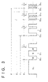
- a quantum-wave interference layer can be made from a serial connection of a number j of partial quantum-wave interference layers I k as shown in FIG. 3.
- ⁇ layers are disposed at an interval D Bk with period T k in each partial interference layers and the number j corresponds to the kinetic energy of electrons.
- the ⁇ layers may be arranged at an interval from D B1 to D Bj in series and may be formed in the second layer B so as to make the partial quantum-wave interference layers and the plurality of the partial quantum-wave interference layers, arranged in series as shown in FIG. 4.
- the eighth aspect of the present invention is directed to a quantum-wave interference layer that functions as a reflecting layer and selectively confines carriers in an adjacent layer.
- the quantum-wave interference layer can be designed to confine either electrons or holes selectively.
- the ninth aspect of the present invention or forming a thick second layer B 0 at the side of an incident plane of the quantum-wave interference layer, and effectively prevents conduction by tunneling effects and reflects carriers.
- the quantum-wave interference layer is formed in at least one of the p-type layer and an n-type layer sandwiching an active layer of a light-emitting semiconductor device and effectively realizes confinement of carriers in the active layer and increases output power.
- a quantum-wave interference layer is formed adjacent to a channel of a field effect transistor realizes effective confinement of carriers therein which conduct through the channel so as to improve an amplification factor of the transistor and signal-to-noise (S/N) ratio.
- a quantum-wave interference layer is formed in a photovoltaic device with a pn junction structure and reflects minor carriers to the p-type or n-type layer and prevents drift of the carriers to a reverse direction around the junction, improving opto-electric conversion efficiency.
- FIG. 9 is a sectional view of a light-emitting diode (LED) 100 in which a quantum-wave interference layer is formed in a p-type cladding layer.
- the p-type cladding layer of the LED 100 has a substrate 10 made of gallium arsenide (GaAs).
- GaAs buffer layer 12 of n-type conduction having a thickness generally of 0.3 ⁇ m and an electron concentration of 2 x 10 18 /cm 3 , is formed on the substrate 10.
- An n-Ga 0.51 In 0.49 P contact layer 14 of n-type conduction, having a thickness generally of 0.3 ⁇ m and electron concentration of 2 x 10 18 /cm 3 is formed on the buffer layer 12.
- An electron reflecting layer 20 functioning as a quantum-wave interference layer is formed on the emission layer 18.
- a Ga 0.51 In 0.49 P second contact layer 24 of p-type conduction having a thickness generally of 0.2 ⁇ m and a hole concentration of 2 x 10 18 /cm 3 , is formed on the cladding layer 22.
- a p-GaAs first p-type contact layer of p-type conduction having a thickness generally of 0.1 ⁇ m, is formed on the second contact layer 24.
- the substrate 10 has a diameter of 2.0 inch and the normal direction of its main surface is offset toward [011] axis by 15 degree from plane (100).
- the LED 100 was manufactured by gas source molecular beam epitaxial deposition (GS-MBE), which is an epitaxial growth method performed under extremely a high vacuum condition.
- GS-MBE is different from a conventional MBE, which supplies group III and V elements both from the sources.
- group III elements such as indium (In), gallium (Ga), and aluminum (Al) are supplied from a solid source and group V elements such as arsenic (As) and phosphorus (P) are supplied by heat decomposition of gas material such as AsH 3 and PH 3 .
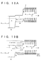
- FIGS. 10A and 10B the n-type cladding layer 16, the emission layer 18, and the electron reflecting layer 20 are shown.
- FIG. 10A shows an energy level of conduction and valence bands on the condition that no external voltage is applied to the LED 100
- FIG. 10B shows the energy level on the condition that the external voltage is applied thereto.
- the electron reflecting layer 20, or a quantum-wave interference layer has a multi-quantum layer structure with 15 periods of a p-Ga 0.51 In 0.49 P well layer as a first layer W and a p-Al 0.51 In 0.49 P barrier layer as a second layer B.
- a ⁇ layer made of p-Al 0.33 Ga 0.33 In 0.33 P is formed at each interface between the first layer W and the second layer B. Thicknesses of the first layer W and the second layer B are respectively determined according to Eqs. 1 and 2. Only the first second layer B 0 is designed to have enough thickness to prevent conduction of carriers by tunneling effects.
- the ⁇ layer is formed to have a thickness of 1.3 nm. Accordingly, electrons injected from the n-type cladding layer 16 into the emission layer 18 are reflected effectively by the electron reflecting layer 20 and confined into the emission layer 18. Although the valence band of the electron reflecting layer 20 also has a multiple period of energy level, holes are designed not to be reflected thereby.
- the respective thickness of the first layer W and the second layer B in the reflecting layer 20 is designed to reflect electrons only. Therefore, holes injected from the p-type cladding layer 22 pass through the electron reflecting layer 20 thus reaching the emission layer 18 easily and being confined therein by the cladding layer 16.
- Luminous intensity was measured by varying the respective thickness of the first layer W and the second layer B.
- FIG. 13 shows a result when the thickness of the second layer B was fixed at 7 nm and that of the first layer W was varied. As shown in FIG. 13, a peak of luminous intensity was obtained when the thickness of the first layer W was 5 nm. Then, luminous intensity was measured fixing the thickness of the first layer W at 5 nm and varying that of the second layer B, the result being shown in FIG. 14. When the second layer B has a thickness of 7 nm, luminous intensity showed its peak.
- the LED 100 with the electron reflecting layer 20 was found to have a maximum luminous intensity when the first layer W had a thickness of 5 nm and the second layer B had a thickness of 7 nm.
- the maximum luminous intensity was eightfold of that of a LED without the electron reflecting layer 20.
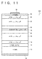
- FIG. 11 shows an LED 200 used in the present embodiment.
- the LED 200 has a hole reflecting layer 32 additionally to the LED 100 structure for reflecting holes.
- the hole reflecting layer 32 is formed between the n-type cladding layer 16 and the emission layer 18 and has a same structure as the electron reflecting layer 20 of the LED 100.
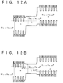
- the thickness of the first layer W is 1.0 nm and that of the second layer B is 1.2 nm.
- FIG. 12A shows an energy level of conduction and valance bands on the condition that no external voltage is applied to the LED 200 and FIG. 12B shows a condition where the external voltage is applied thereto.
- the LED 200 thus obtained provides a luminous intensity of 16 fold compared with an LED with as same structure as the LED 200 but without the electron reflecting layer 20 and the hole reflecting layer 32.
- an LED has a structure as same as that of the LED 100 of FIG. 10A.
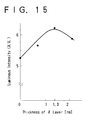
- a thickness of the ⁇ layer is varied in many samples and a measured luminous intensity of the LED for the various thicknesses is shown in FIG. 15.
- the luminous intensity reaches its peak when the thickness of the ⁇ layer is about 1.3 nm while the thicknesses of the first layer W and the second layer B are 5.6 nm and 7.5 nm, respectively, which slightly differed from the optimized thickness in Example 1.
- the obtained luminous intensity of the LED 300 was 1.5 fold of that of an LED without the ⁇ layer.
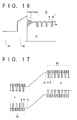
- FIG. 16 is an energy diagram of a MOSFET according to the present embodiment.
- a conventional MOSFET has a channel of an inversion layer just beneath an insulation film 40, conducting minor carriers through the channel.
- a larger voltage is applied to a gate electrode 42 of the conventional MOSFET and thus more carriers in the channel of the inversion layer overflow.
- signal-to-noise (S/N) ratio decreases.
- a quantum-wave interference layer 20 was formed below the channel as shown in FIG. 16 having a multi-layer structure with arbitrary periods including the second layer B made of silicon (Si) and the first layer W made of Ge. As a result, more carriers were confined in the channel of the inversion layer.
- the most preferable thickness of the second layer B was 6.8 nm and that of the first layer W was 2.0 nm.
- a quantum-wave interference layer can be formed in a photovoltaic device with a pn junction structure.
- an electron reflecting layer 20 is formed in a p-layer
- a hole reflecting layer 32 is formed in an n-layer.
- pairs of an electron and a hole are formed.
- Most of the electrons in the conventional device are accelerated to the n-layer due to potential declination of conduction bands while the rest of the electrons drift to the p-layer so as not to contribute to induction of voltage. The larger the intensity of the incident light becomes, the more electrons overflow to the player.
- the electron reflecting layer 20, or a quantum-wave interference layer was formed in the p-layer in this embodiment.
- drifting of electrons were prevented, which enabled more electrons to conduct to the n-layer.
- some of holes do not contribute to induction of voltage on account of holes drifting to the n-layer in a conventional element.
- the hole reflecting layer 32, or a quantum-wave interference layer was formed in the n-layer. As a result, drifting of holes were prevented and enabled more holes to conduct to the p-layer. Consequently, leakage of current was minimized and efficiency of electro-optic conversion was improved.
- the quantum-wave interference layer can be applied to a laser diode.
- the quantum-wave interference layer was formed to have a multi-layer structure made of ternary compounds including Ga 0.51 In 0.49 P and Al 0.51 In 0.49 P.
- the interference layer can be made of quaternary compounds such as Al x Ga y In 1-x-y P, selecting arbitrary composition ratio within the range of 0 ⁇ x ⁇ 1, 0 ⁇ y ⁇ 1, and 0 ⁇ x+y ⁇ 1.
- the quantum-wave interference layer can be made of group III-V compound semiconductor, group II-VI compound semiconductors, Si and Ge, and semiconductors of other hetero-material.
- a semiconductor device is constituted by a quantum-wave interference layer with plural periods of a pair of a first layer W and a second layer B.
- the second layer B has wider band gap than the first layer W.
- Each thickness of the first layer W and the second layer B is determined by multiplying by an odd number one fourth of wavelength of quantum-wave of carriers in each of the first layer W and the second layer B existing around the lowest energy level of the second layer B.
- a ⁇ layer, for sharply varying energy band, is formed at an every interface between the first layer W and the second layer B and has a thickness substantially thinner than the first layer W and the second layer B.
- the quantum-wave interference layer functions as a reflecting layer of carriers for higher reflectivity.
Landscapes
- Physics & Mathematics (AREA)
- Optics & Photonics (AREA)
- Nanotechnology (AREA)
- Engineering & Computer Science (AREA)
- Chemical & Material Sciences (AREA)
- Electromagnetism (AREA)
- Life Sciences & Earth Sciences (AREA)
- Biophysics (AREA)
- General Physics & Mathematics (AREA)
- Condensed Matter Physics & Semiconductors (AREA)
- Crystallography & Structural Chemistry (AREA)
- Geometry (AREA)
- Led Devices (AREA)
- Semiconductor Lasers (AREA)
- Insulated Gate Type Field-Effect Transistor (AREA)
- Light Receiving Elements (AREA)
- Photovoltaic Devices (AREA)
Applications Claiming Priority (3)
| Application Number | Priority Date | Filing Date | Title |
|---|---|---|---|
| JP12348197A JP3014339B2 (ja) | 1997-04-25 | 1997-04-25 | 量子波干渉層を有した半導体素子 |
| JP123481/97 | 1997-04-25 | ||
| JP12348197 | 1997-04-25 |
Publications (2)
| Publication Number | Publication Date |
|---|---|
| EP0874403A2 true EP0874403A2 (de) | 1998-10-28 |
| EP0874403A3 EP0874403A3 (de) | 2003-11-05 |
Family
ID=14861709
Family Applications (1)
| Application Number | Title | Priority Date | Filing Date |
|---|---|---|---|
| EP98106816A Withdrawn EP0874403A3 (de) | 1997-04-25 | 1998-04-15 | Halbleiteranordnungen mit Quanten-Welle-Interferenz-Schichten |
Country Status (3)
| Country | Link |
|---|---|
| US (2) | US6175123B1 (de) |
| EP (1) | EP0874403A3 (de) |
| JP (1) | JP3014339B2 (de) |
Cited By (7)
| Publication number | Priority date | Publication date | Assignee | Title |
|---|---|---|---|---|
| EP0935294A1 (de) * | 1998-02-06 | 1999-08-11 | Canare Electric Co., Ltd. | Bauelement mit variabler Kapazität und mit Quantenwellen-Interferenz-Schichten |
| EP0996166A3 (de) * | 1998-10-21 | 2003-11-05 | Canare Electric Co., Ltd. | Halbleiteranordnungen mit einer Mehrfach-Quantenbarrierestruktur |
| EP1011150A3 (de) * | 1998-12-17 | 2004-01-02 | Canare Electric Co., Ltd. | Lichtempfindliche Anordnung mit Quantenwelleninterferenzschichten |
| EP0996168A3 (de) * | 1998-10-23 | 2004-01-14 | Canare Electric Co., Ltd. | Feldeffektransistor mit einer Mehrfach-Quantenbarrierestruktur |
| EP1883119A2 (de) | 2006-07-27 | 2008-01-30 | Osram Opto Semiconductors GmbH | Halbleiter-Schichtstruktur mit Übergitter |
| US7822089B2 (en) | 2006-07-27 | 2010-10-26 | Osram Opto Semiconductors Gmbh | Semiconductor layer structure with superlattice |
| US7893424B2 (en) | 2006-07-27 | 2011-02-22 | Osram Opto Semiconductors Gmbh | Semiconductor layer structure with superlattice |
Families Citing this family (13)
| Publication number | Priority date | Publication date | Assignee | Title |
|---|---|---|---|---|
| EP0954034A3 (de) | 1998-04-28 | 2000-01-26 | Canare Electric Co., Ltd. | Lichtempfänger mit Quantenwelleninterferenzschichten |
| JP2000133655A (ja) * | 1998-10-23 | 2000-05-12 | Canare Electric Co Ltd | 量子波干渉層を有するトランジスタ |
| JP4119158B2 (ja) * | 2002-04-23 | 2008-07-16 | 三菱電機株式会社 | 傾斜状多重量子バリアを用いた半導体発光素子 |
| WO2004084279A1 (en) * | 2003-03-14 | 2004-09-30 | Midwest Research Institute | Wafer characteristics via reflectometry |
| WO2005020396A1 (ja) * | 2003-08-26 | 2005-03-03 | Sony Corporation | GaN系III−V族化合物半導体発光素子及びその製造方法 |
| JP2009540616A (ja) * | 2006-06-12 | 2009-11-19 | スリーエム イノベイティブ プロパティズ カンパニー | 再発光半導体構造物を有するled装置及び集束光学要素 |
| US7952110B2 (en) * | 2006-06-12 | 2011-05-31 | 3M Innovative Properties Company | LED device with re-emitting semiconductor construction and converging optical element |
| US20070284565A1 (en) * | 2006-06-12 | 2007-12-13 | 3M Innovative Properties Company | Led device with re-emitting semiconductor construction and optical element |
| WO2007146860A1 (en) * | 2006-06-12 | 2007-12-21 | 3M Innovative Properties Company | Led device with re-emitting semiconductor construction and optical element |
| US7902542B2 (en) * | 2006-06-14 | 2011-03-08 | 3M Innovative Properties Company | Adapted LED device with re-emitting semiconductor construction |
| US8022292B2 (en) | 2006-10-02 | 2011-09-20 | SolASE Corporation | Photovoltaic device employing a resonator cavity |
| KR20120129029A (ko) * | 2011-05-18 | 2012-11-28 | 엘지이노텍 주식회사 | 발광 소자 |
| KR20120138080A (ko) * | 2011-06-14 | 2012-12-24 | 엘지이노텍 주식회사 | 발광 소자 |
Family Cites Families (12)
| Publication number | Priority date | Publication date | Assignee | Title |
|---|---|---|---|---|
| JPS6028268A (ja) * | 1983-07-26 | 1985-02-13 | Agency Of Ind Science & Technol | 半導体装置 |
| US4814837A (en) * | 1986-03-13 | 1989-03-21 | The United States Of America As Represented By The Secretary Of The Navy | Quantum well electron barrier diode |
| JPH0666519B2 (ja) | 1986-08-14 | 1994-08-24 | 東京工業大学長 | 超格子構造体 |
| JPH01181578A (ja) * | 1988-01-12 | 1989-07-19 | Mitsubishi Electric Corp | アバランシ・ホトダイオード |
| EP0444134A4 (en) * | 1988-11-16 | 1993-03-03 | Gaylord, Thomas K | Solid state, quantum mechanical, electron and hole wave devices |
| CA2055208C (en) | 1990-11-09 | 2000-07-04 | Michinori Irikawa | A quatum barrier semiconductor optical device |
| EP0506127B1 (de) * | 1991-03-28 | 1999-06-09 | Nec Corporation | Halbleiterphotodetektor mit Lawinenmultiplikation |
| US5789760A (en) * | 1992-05-08 | 1998-08-04 | The Furukawa Electric Co., Ltd. | Multiquantum barrier Schottky junction device |
| JPH06204457A (ja) | 1992-05-08 | 1994-07-22 | Furukawa Electric Co Ltd:The | 多重量子障壁ショットキー接合素子 |
| JPH06260493A (ja) * | 1993-03-05 | 1994-09-16 | Mitsubishi Electric Corp | 半導体装置 |
| JPH07147449A (ja) | 1993-11-25 | 1995-06-06 | Mitsubishi Electric Corp | 多重量子障壁構造,及び可視光半導体レーザダイオード |
| JPH0888434A (ja) * | 1994-09-19 | 1996-04-02 | Mitsubishi Electric Corp | 半導体レーザ,及びその製造方法 |
-
1997
- 1997-04-25 JP JP12348197A patent/JP3014339B2/ja not_active Expired - Fee Related
-
1998
- 1998-04-14 US US09/059,374 patent/US6175123B1/en not_active Expired - Fee Related
- 1998-04-15 EP EP98106816A patent/EP0874403A3/de not_active Withdrawn
-
2000
- 2000-10-25 US US09/695,312 patent/US6476412B1/en not_active Expired - Fee Related
Cited By (12)
| Publication number | Priority date | Publication date | Assignee | Title |
|---|---|---|---|---|
| EP0935294A1 (de) * | 1998-02-06 | 1999-08-11 | Canare Electric Co., Ltd. | Bauelement mit variabler Kapazität und mit Quantenwellen-Interferenz-Schichten |
| US6331716B1 (en) | 1998-02-06 | 2001-12-18 | Canare Electric Co., Ltd. | Variable capacity device with quantum-wave interference layers |
| EP0996166A3 (de) * | 1998-10-21 | 2003-11-05 | Canare Electric Co., Ltd. | Halbleiteranordnungen mit einer Mehrfach-Quantenbarrierestruktur |
| EP0996168A3 (de) * | 1998-10-23 | 2004-01-14 | Canare Electric Co., Ltd. | Feldeffektransistor mit einer Mehrfach-Quantenbarrierestruktur |
| EP1011150A3 (de) * | 1998-12-17 | 2004-01-02 | Canare Electric Co., Ltd. | Lichtempfindliche Anordnung mit Quantenwelleninterferenzschichten |
| US6818916B2 (en) | 1998-12-17 | 2004-11-16 | Canare Electric Co., Ltd. | Light-receiving device with quantum-wave interference layers |
| EP1883119A2 (de) | 2006-07-27 | 2008-01-30 | Osram Opto Semiconductors GmbH | Halbleiter-Schichtstruktur mit Übergitter |
| EP1883119A3 (de) * | 2006-07-27 | 2008-11-26 | OSRAM Opto Semiconductors GmbH | Halbleiter-Schichtstruktur mit Übergitter |
| US7822089B2 (en) | 2006-07-27 | 2010-10-26 | Osram Opto Semiconductors Gmbh | Semiconductor layer structure with superlattice |
| US7893424B2 (en) | 2006-07-27 | 2011-02-22 | Osram Opto Semiconductors Gmbh | Semiconductor layer structure with superlattice |
| US8022392B2 (en) | 2006-07-27 | 2011-09-20 | Osram Opto Semiconductors Gmbh | Semiconductor layer structure with superlattice |
| US8471240B2 (en) | 2006-07-27 | 2013-06-25 | Osram Opto Semiconductors Gmbh | Semiconductor layer structure with superlattice |
Also Published As
| Publication number | Publication date |
|---|---|
| JPH10303406A (ja) | 1998-11-13 |
| US6476412B1 (en) | 2002-11-05 |
| US6175123B1 (en) | 2001-01-16 |
| JP3014339B2 (ja) | 2000-02-28 |
| EP0874403A3 (de) | 2003-11-05 |
Similar Documents
| Publication | Publication Date | Title |
|---|---|---|
| US6175123B1 (en) | Semiconductor devices with quantum-wave interference layers | |
| US5475700A (en) | Laser diode with electron and hole confinement and barrier layers | |
| US6664561B2 (en) | Light-receiving device with quantum-wave interference layers | |
| JP3486193B2 (ja) | 光電半導体素子 | |
| US6479842B1 (en) | Field effect transistor with a quantum-wave interference layer | |
| US6188082B1 (en) | Diodes with quantum-wave interference layers | |
| US6188083B1 (en) | Diodes with quantum-wave interference layers | |
| US6552412B2 (en) | Semiconductor device with quantum-wave interference layers | |
| US6486490B1 (en) | Light-emitting device with a quantum-wave interference layer | |
| EP0996166A2 (de) | Halbleiteranordnungen mit einer Mehrfach-Quantenbarrierestruktur | |
| US6417520B1 (en) | Semiconductor device with quantum-wave interference layers | |
| US6331716B1 (en) | Variable capacity device with quantum-wave interference layers | |
| US6337508B1 (en) | Transistor with a quantum-wave interference layer | |
| US6420727B1 (en) | Light-emitting semiconductor device with quantum-wave interference layers | |
| US6818916B2 (en) | Light-receiving device with quantum-wave interference layers | |
| EP1085583A2 (de) | Halbleiteranordnungen mit Quantenwelleninterferenzschichten | |
| EP0967658A2 (de) | Halbleiteranordnung mit Quanten-Wellen-Interferenz-Schichten | |
| EP0996169A2 (de) | Halbleiteranordnung mit einer Begrenzungsschicht | |
| JP2000114601A (ja) | 量子波干渉層を有した半導体素子及び半導体素子を構成する量子波干渉層の設計方法 | |
| EP1011147A2 (de) | Transistoren mit einer Quantenwelleninterferenzschicht | |
| EP1085582A2 (de) | Lichtemittierende Halbleiteranordnung mit Quantenwelleninterferenzschichten | |
| JP3466526B2 (ja) | 量子波干渉層を有するトランジスタ |
Legal Events
| Date | Code | Title | Description |
|---|---|---|---|
| PUAI | Public reference made under article 153(3) epc to a published international application that has entered the european phase |
Free format text: ORIGINAL CODE: 0009012 |
|
| AK | Designated contracting states |
Kind code of ref document: A2 Designated state(s): AT BE CH CY DE DK ES FI FR GB GR IE IT LI LU MC NL PT SE |
|
| AX | Request for extension of the european patent |
Free format text: AL;LT;LV;MK;RO;SI |
|
| RAP1 | Party data changed (applicant data changed or rights of an application transferred) |
Owner name: CANARE ELECTRIC CO., LTD. |
|
| RIC1 | Information provided on ipc code assigned before grant |
Free format text: 7H 01L 29/15 A, 7H 01L 33/00 B, 7H 01L 29/78 B, 7H 01L 31/068 B, 7H 01L 31/0304 B, 7H 01S 3/19 B |
|
| PUAL | Search report despatched |
Free format text: ORIGINAL CODE: 0009013 |
|
| AK | Designated contracting states |
Kind code of ref document: A3 Designated state(s): AT BE CH CY DE DK ES FI FR GB GR IE IT LI LU MC NL PT SE |
|
| AX | Request for extension of the european patent |
Extension state: AL LT LV MK RO SI |
|
| 17P | Request for examination filed |
Effective date: 20040413 |
|
| AKX | Designation fees paid |
Designated state(s): DE FR GB |
|
| STAA | Information on the status of an ep patent application or granted ep patent |
Free format text: STATUS: THE APPLICATION IS DEEMED TO BE WITHDRAWN |
|
| 18D | Application deemed to be withdrawn |
Effective date: 20051101 |