EP0873557B1 - Mehrfarbiges licht abstrahlende bildanzeigevorrichtung - Google Patents
Mehrfarbiges licht abstrahlende bildanzeigevorrichtung Download PDFInfo
- Publication number
- EP0873557B1 EP0873557B1 EP97947022A EP97947022A EP0873557B1 EP 0873557 B1 EP0873557 B1 EP 0873557B1 EP 97947022 A EP97947022 A EP 97947022A EP 97947022 A EP97947022 A EP 97947022A EP 0873557 B1 EP0873557 B1 EP 0873557B1
- Authority
- EP
- European Patent Office
- Prior art keywords
- light
- display device
- image display
- semiconductor light
- emitting diodes
- Prior art date
- Legal status (The legal status is an assumption and is not a legal conclusion. Google has not performed a legal analysis and makes no representation as to the accuracy of the status listed.)
- Expired - Lifetime
Links
Images
Classifications
-
- H—ELECTRICITY
- H04—ELECTRIC COMMUNICATION TECHNIQUE
- H04N—PICTORIAL COMMUNICATION, e.g. TELEVISION
- H04N9/00—Details of colour television systems
- H04N9/12—Picture reproducers
- H04N9/30—Picture reproducers using solid-state colour display devices
-
- H—ELECTRICITY
- H10—SEMICONDUCTOR DEVICES; ELECTRIC SOLID-STATE DEVICES NOT OTHERWISE PROVIDED FOR
- H10H—INORGANIC LIGHT-EMITTING SEMICONDUCTOR DEVICES HAVING POTENTIAL BARRIERS
- H10H20/00—Individual inorganic light-emitting semiconductor devices having potential barriers, e.g. light-emitting diodes [LED]
- H10H20/80—Constructional details
- H10H20/85—Packages
- H10H20/851—Wavelength conversion means
-
- H—ELECTRICITY
- H10—SEMICONDUCTOR DEVICES; ELECTRIC SOLID-STATE DEVICES NOT OTHERWISE PROVIDED FOR
- H10W—GENERIC PACKAGES, INTERCONNECTIONS, CONNECTORS OR OTHER CONSTRUCTIONAL DETAILS OF DEVICES COVERED BY CLASS H10
- H10W90/00—Package configurations
Definitions
- the invention relates to a multi-colored light emitting Image display device, in particular a high-resolution Image display device, with a monolithically integrated Arrangement.
- the invention has for its object a technological Easy to manufacture, multi-color light-emitting image display device of the type mentioned at the beginning to deliver.
- a carrier is provided on or in the a variety of individually electronically controllable Semiconductor light-emitting diodes or laser diodes is formed, and a plurality of the semiconductor light emitting diodes or laser diodes of optically separated luminescence conversion elements associated with phosphors of different colors is, each at least a part of one of the Semiconductor light emitting diodes or laser diodes emitted light absorb, convert to visible light of a different wavelength and radiate.
- the Semiconductor light-emitting diodes or laser diodes in the ultraviolet or blue wavelength range.
- the special one Advantage of a semiconductor light emitting diode emitting in the UV wavelength range or laser diode is that they no or significantly less visible and therefore possibly emits disturbing residual radiation.
- one in the UV wavelength range can be a blue light emitting Semiconductor light-emitting diode or laser diode used become.
- those applied to the carrier Luminescence conversion elements alternating with Phosphors of the primary colors are equipped, which so are selected so that when irradiated in particular with UV light covers the entire visible spectrum.
- dyes for the luminescence conversion elements shining in the primary colors red, green and blue ZnS: Ag, ZnS: Cu, Al or ZnCdS: Ag be used.
- phosphors Phosphors such as YAG: Ce and others with rare ones Soil doped garnets, thiogallates, aluminates or orthosilicates be used.
- Semiconductor light-emitting diodes or laser diodes are the Luminescence conversion elements alternating with phosphors of the three basic colors red, green and blue.
- Luminescence conversion elements alternating with phosphors of the three basic colors red, green and blue.
- blue light-emitting semiconductor light-emitting diodes or -Laser diodes are only the two primary colors Green and red needed for the luminescence conversion elements because the basic color blue is already from the light emitting diodes or laser diodes is emitted.
- the invention can provide that the luminescence conversion elements on that of the semiconductor light emitting diode or laser diode device opposite side of the carrier applied are.
- the transparent or at least translucent straps through a sapphire substrate is trained.
- the advantage as a substrate material Sapphire used is relatively inexpensive in large Areas available (typically are disc diameters available from three inches and more) and offers due to its extremely high mechanical stability which in addition to the electronic properties simultaneously required mechanical Characteristics.
- the carrier also consist of opaque material and / or with a be provided over the entire surface with which the loss portion of the unusable light output is reduced can be.
- the mirror layer expediently on the back of the Carrier, that is on the luminescence conversion elements opposite side of the carrier applied.
- a contact layer made of transparent or at least translucent Material provided.
- the normally opaque In this case, connecting cables only cover part of the connection area for the semiconductor light-emitting diodes or laser diodes. To broaden electricity and thus optimal coupling of the electrical current then serves this transparent or at least translucent contact layer.
- the dyes of the luminescence conversion elements can expediently directly on this transparent contact layer, or also on an intermediate layer, or embedded be applied in a special sealing compound.
- the base material of the monolithically integrated semiconductor light emitting diodes or laser diodes gallium nitride GaN or a derivative thereof, such as InGaN or AlGaN. Since that Semiconductor material GaN also for applications in power electronics is suitable, this training enables at the same time an integration of line driver circuits or electronic control circuits.
- the semiconductor light-emitting diodes or laser diodes formed on or in the carrier have a layer sequence of semiconductor materials, in particular a layer sequence with an active layer of Ga x In 1-x N or Ga x Al 1-x N which emit electromagnetic radiation with a wavelength of less than or equal to 480 nm, in particular less than or equal to 370 nm, the luminescence conversion element emitting radiation from a first wavelength range into radiation from a second spectral region of the radiation emitted by the light-emitting diodes or laser diodes Converts wavelength range.
- the luminescence conversion element spectrally selectively absorbs a radiation emitted by the light-emitting diodes and emits it in the longer-wave range (in the second wavelength range).
- the radiation emitted by the light-emitting diodes has a radiation maximum at a wavelength of less than or equal to 370 nm.
- a particular advantage of the image display device according to the invention is also that the wavelength spectrum generated by luminescence conversion and thus the color of the emitted light do not depend on the level of the operating current through the semiconductor light-emitting diodes or laser diodes. This is particularly important when the ambient temperature of the semiconductor component and thus, as is known, also the operating current fluctuates greatly.
- Light-emitting diodes with a semiconductor body based on GaN are particularly sensitive in this regard.
- the image display device according to the invention only requires a single control voltage and thus also only a single control circuit arrangement, as a result of which the component expenditure can be kept very low.
- Image display devices are the luminescence conversion element or another radiation-transmissive component the component coating additionally light-scattering particles, so-called diffusers added. This allows advantageously the color impression and the radiation characteristic optimize the image display device.
- UV light with wavelengths of less than or equal to 370 nm is a complete conversion of UV light by the Luminescence conversion elements are not required because of the ultraviolet Do not contribute to color changes in the visible Spectrum leads.
- Luminescence conversion elements can be sealed with a UV-opaque lacquer or by mounting the image display device behind a pane of glass if necessary remaining portion of the emitted UV light simply filtered out become.
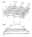
- the image display devices shown in Figures 1 and 2 comprise a monolithically integrated arrangement 1, a so-called array consisting of a transparent or at least translucent support 2 from a large area Sapphire substrate, which is relatively inexpensive to use Disc diameters of typically three inches and more is available, a semiconductor light source consisting of GaN base material with a variety of matrix-like the carrier 2 arranged, electronically individually controllable, semiconductor light emitting diodes emitting in the UV wavelength range or laser diodes 4, each of which is an n-type Region 3A and a p-type region 3B, as well as a variety of luminescence conversion elements 5, 6, 7 with phosphors of different colors, the that of the semiconductor light emitting diodes or laser diodes 4 in UV wavelength range emitted light 8 received, in convert visible light 9 and as shown schematically Radiate in a direction transverse to the plane of the sapphire carrier 2.
- each luminescence conversion element 5 is a phosphor Basic color red
- each luminescence conversion element 6 one Fluorescent of the basic color green
- each luminescence conversion element 7 a phosphor of the basic color blue.
- Each represents a triple of the luminescence conversion elements 5, 6, 7 thus a pixel of the image display device and enables the emission of full-color images, whereby in a manner known per se by means of suitable phosphors the entire visible spectrum is shown for three primary colors can be.
- the three preferred used Basic colors red, green and blue are of course also other suitable basic colors can be realized without the basic principle to leave the invention.
- Suitable materials for the dyes of the three primary colors red, green and blue luminous luminescence conversion elements 5, 6, 7 are for example ZnS: Ag, ZnS: Cu, Al and ZnCdS: Ag.
- the semiconductor light emitting diodes emitting in the UV wavelength range 4 comprise by means of semiconductor technology manufacturing steps known per se immediately on one Side of the carrier 2 columns 10 structured in strip form made of n-doped GaN material on which to form a pn junction or UV light generating region 11 p-doped GaN material 12 structured to form rows is.
- the electronic control of the individual LEDs or laser diodes 4 takes place via metallic column lines 13 and row lines 14 in the form of metal tracks, which with known semiconductor technology structuring and manufacturing measures are manufactured, and which for Control of the individual pixels with column and row address signals from a (not shown) Control circuit are supplied.
- Each luminescence conversion element can, for example, consist of a transparent epoxy resin or also silicone, thermoplastic or thermoset material, which with suitable provided organic or inorganic dye molecules is.
- inorganic ones can advantageously be used Distribute phosphors homogeneously in epoxy resin in a simple manner.
- the luminescence conversion elements 5, 6, 7 are shown in constant strength and preferably with the same base areas by screen printing or other inexpensive Process applied to the carrier 2.
- the semiconductor light-emitting diodes are 4 and the luminescence conversion elements 5, 6, 7 formed on both sides of the plate-shaped carrier 2.
- the carrier consists of a transparent or at least translucent material such as sapphire.
- the light-emitting diodes are 4 and the luminescence conversion elements 5 on the same Side of the carrier arranged.
- This design has above all then advantages if the selectivity between the individual Color pixels, for example, due to a thicker support should not be sufficient.
- the row lines 14 for the electrical connection of the p-type region 3B each In this case, LED 4 covers only part of the upper, p-type region 3B.
- transparent contact layers 15 made of electrically conductive material provided the p-type region 3B each Cover LED 4. This is on the contact layer 15 Luminescence conversion element 5 arranged; at the illustrated Execution is the dye 16 directly on the contact layer 15 applied and with a transparent cover layer 17 coated.
- the material for the electrically conductive Transparent contact layer 15 can, for example, indium tin oxide exhibit; alternatively, the contact layer 15 also consist of a thin, transparent gold layer.
- the dye can also be used in a synthetic resin or similar suitable material can be embedded, which Material the contact layer 15 (and possibly one covers a small part of the row line 14).
- the Back of the carrier 2 over a large area with a mirror layer 18 be provided.
Landscapes
- Engineering & Computer Science (AREA)
- Multimedia (AREA)
- Signal Processing (AREA)
- Led Device Packages (AREA)
- Led Devices (AREA)
- Devices For Indicating Variable Information By Combining Individual Elements (AREA)
- Semiconductor Lasers (AREA)
Abstract
Description
- Figur 1
- eine schematische Darstellung einer hochauflösenden, mehrfarbiges Licht abstrahlenden Bildanzeigevorrichtung, eines sogenannten True Color Displays; und
- Figur 2
- eine schematische Schnittansicht einer weiteren Ausführungsform eines True Color Displays, bei der die Leuchtdioden und die Lumineszenzkonversionselemente auf derselben Seite eines vollflächig verspiegelten Trägers ausgebildet sind.
- 1
- monolithisch integrierte Anordnung
- 2
- Träger
- 3A
- n-leitender Bereich
- 3B
- p-leitender Bereich
- 4
- Halbleiter-Leuchtdioden oder -Laserdioden
- 5, 6, 7
- Lumineszenzkonversionselemente
- 8
- emittiertes Licht
- 9
- sichtbares Licht
- 10
- Spalten
- 11
- pn-Übergang
- 12
- GaN-Material
- 13
- Spaltenleitungen
- 14
- Zeilenleitungen
- 15
- Kontaktschichten
- 16
- Farbstoff
- 17
- Deckschicht
- 18
- Spiegelschicht
Claims (9)
- Mehrfarbiges Licht abstrahlende Bildanzeigevorrichtung worin ein Träger (2) vorgesehen ist, auf bzw. in dem eine Vielzahl von jeweils einzeln elektronisch ansteuerbaren Halbleiter-Leuchtdioden (4) oder -Laserdioden ausgebildet ist, wobei den Halbleiter-Leuchtdioden (4) oder Laserdioden (3) eine Mehrzahl von optisch voneinander getrennten Lumineszenzkonversionselementen (5, 6, 7) mit Leuchtstoffen unterschiedlicher Farbe zugeordnet ist, die jeweils zumindest einen Teil eines von den Halbleiter-Leuchtdioden (4) oder -Laserdioden emittierten Lichtes (8) absorbieren, in sichtbares Licht (9) anderer Wellenlänge umwandeln und abstrahlen.
- Bildanzeigevorrichtung nach Anspruch 1, dadurch gekennzeichnet, dass die Halbleiter-Leuchtdioden (4) oder -Laserdioden im ultravioletten oder blauen Wellenlängenbereich emittieren.
- Bildanzeigevorrichtung nach einem der Ansprüche 1 bis 2, dadurch gekennzeichnet, dass die auf bzw. in dem Träger (2) aufgebrachten Lumineszenzkonversionselemente (5, 6, 7) abwechselnd mit Leuchtstoffen der wenigstens zwei Grundfarben Rot und Grün oder der drei Grundfarben Rot, Grün und Blau ausgestattet sind.
- Bildanzeigevorrichtung nach Anspruch 3, dadurch gekennzeichnet, dass als Farbstoffe für die in den Grundfarben Rot, Grün, Blau leuchtenden Lumineszenzkonversionselemente (5, 6, 7) ZnS:Ag, ZnS:Cu,Al bzw. ZnCdS:Ag verwendet wird.
- Bildanzeigevorrichtung nach einem der Ansprüche 1 bis 4, dadurch gekennzeichnet, dass das Grundmaterial der auf bzw. in dem Träger monolithisch integrierten Halbleiter-Leuchtdioden oder -Laserdioden (3) GaN aufweist.
- Bildanzeigevorrichtung nach einem der Ansprüche 1 bis 5, dadurch gekennzeichnet, dass der Träger (2) durchsichtig bzw. wenigstens durchscheinend ausgebildet ist und dass die Lumineszenzkonversionselemente (5, 6, 7) auf der den Halbleiter-Leuchtdioden oder -Laserdioden (4) abgewandten Seite des Trägers (2) aufgebracht sind.
- Bildanzeigevorrichtung nach einem der Ansprüche 1 bis 5, dadurch gekennzeichnet, dass die Lumineszenzkonversionselemente (5, 6, 7) auf derselben Seite des Trägers (2) wie die Halbleiter-Leuchtdioden (4) oder Laserdioden aufgebracht sind, und eine durchsichtige bzw. wenigstens durchscheinende, elektrisch leitende Kontaktschicht (15) für die einzelnen elektronisch ansteuerbaren Halbleiter-Leuchtdioden (4) oder Laserdioden vorgesehen ist.
- Bildanzeigevorrichtung nach einem der Ansprüche 1 bis 7, dadurch gekennzeichnet, dass der Träger (2) großflächig verspiegelt ist.
- Bildanzeigevorrichtung nach einem der Ansprüche 1 bis 8, dadurch gekennzeichnet, dass die Vielzahl der auf dem Träger (2) ausgebildeten Halbleiter-Leuchtdioden oder -Laserdioden (4) zeilen- und spaltenweise angeordnet und elektrisch ansteuerbar sind.
Applications Claiming Priority (3)
| Application Number | Priority Date | Filing Date | Title |
|---|---|---|---|
| DE19645035 | 1996-10-31 | ||
| DE19645035A DE19645035C1 (de) | 1996-10-31 | 1996-10-31 | Mehrfarbiges Licht abstrahlende Bildanzeigevorrichtung |
| PCT/DE1997/002478 WO1998019290A1 (de) | 1996-10-31 | 1997-10-24 | Mehrfarbiges licht abstrahlende bildanzeigevorrichtung |
Publications (2)
| Publication Number | Publication Date |
|---|---|
| EP0873557A1 EP0873557A1 (de) | 1998-10-28 |
| EP0873557B1 true EP0873557B1 (de) | 2000-08-16 |
Family
ID=7810368
Family Applications (1)
| Application Number | Title | Priority Date | Filing Date |
|---|---|---|---|
| EP97947022A Expired - Lifetime EP0873557B1 (de) | 1996-10-31 | 1997-10-24 | Mehrfarbiges licht abstrahlende bildanzeigevorrichtung |
Country Status (6)
| Country | Link |
|---|---|
| US (1) | US5994722A (de) |
| EP (1) | EP0873557B1 (de) |
| JP (2) | JP2000505915A (de) |
| CN (1) | CN1212069A (de) |
| DE (2) | DE19645035C1 (de) |
| WO (1) | WO1998019290A1 (de) |
Families Citing this family (112)
| Publication number | Priority date | Publication date | Assignee | Title |
|---|---|---|---|---|
| DE19638667C2 (de) * | 1996-09-20 | 2001-05-17 | Osram Opto Semiconductors Gmbh | Mischfarbiges Licht abstrahlendes Halbleiterbauelement mit Lumineszenzkonversionselement |
| EP1441395B9 (de) | 1996-06-26 | 2012-08-15 | OSRAM Opto Semiconductors GmbH | Lichtabstrahlendes Halbleiterbauelement mit Lumineszenzkonversionselement |
| US5895932A (en) * | 1997-01-24 | 1999-04-20 | International Business Machines Corporation | Hybrid organic-inorganic semiconductor light emitting diodes |
| AU747260B2 (en) | 1997-07-25 | 2002-05-09 | Nichia Chemical Industries, Ltd. | Nitride semiconductor device |
| US6252254B1 (en) | 1998-02-06 | 2001-06-26 | General Electric Company | Light emitting device with phosphor composition |
| US6366018B1 (en) | 1998-10-21 | 2002-04-02 | Sarnoff Corporation | Apparatus for performing wavelength-conversion using phosphors with light emitting diodes |
| US6404125B1 (en) * | 1998-10-21 | 2002-06-11 | Sarnoff Corporation | Method and apparatus for performing wavelength-conversion using phosphors with light emitting diodes |
| US6429583B1 (en) | 1998-11-30 | 2002-08-06 | General Electric Company | Light emitting device with ba2mgsi2o7:eu2+, ba2sio4:eu2+, or (srxcay ba1-x-y)(a1zga1-z)2sr:eu2+phosphors |
| JP3770014B2 (ja) | 1999-02-09 | 2006-04-26 | 日亜化学工業株式会社 | 窒化物半導体素子 |
| ATE452445T1 (de) | 1999-03-04 | 2010-01-15 | Nichia Corp | Nitridhalbleiterlaserelement |
| US6696703B2 (en) * | 1999-09-27 | 2004-02-24 | Lumileds Lighting U.S., Llc | Thin film phosphor-converted light emitting diode device |
| JP2001111109A (ja) * | 1999-10-07 | 2001-04-20 | Sharp Corp | 窒化ガリウム系化合物半導体発光素子 |
| US7202506B1 (en) * | 1999-11-19 | 2007-04-10 | Cree, Inc. | Multi element, multi color solid state LED/laser |
| US8829546B2 (en) | 1999-11-19 | 2014-09-09 | Cree, Inc. | Rare earth doped layer or substrate for light conversion |
| US6291841B1 (en) * | 2000-01-10 | 2001-09-18 | Jiahn-Chang Wu | Flat interconnection semiconductor package |
| US6737801B2 (en) * | 2000-06-28 | 2004-05-18 | The Fox Group, Inc. | Integrated color LED chip |
| JP2002280607A (ja) * | 2001-01-10 | 2002-09-27 | Toyoda Gosei Co Ltd | 発光装置 |
| RU2202843C2 (ru) * | 2001-04-27 | 2003-04-20 | Институт проблем химической физики РАН | Полупроводниковый электролюминесцентный источник света с перестраиваемым цветом свечения |
| US6795455B2 (en) | 2001-08-14 | 2004-09-21 | The United States Of America As Represented By The Secretary Of The Navy | All solid-state RGB and white light generator |
| US6680579B2 (en) * | 2001-12-14 | 2004-01-20 | Hewlett-Packard Development Company, L.P. | Method and apparatus for image and video display |
| KR100567548B1 (ko) * | 2002-04-22 | 2006-04-05 | 서울반도체 주식회사 | 백색 칩 발광 다이오드 및 그 제조 방법 |
| US6821799B2 (en) | 2002-06-13 | 2004-11-23 | University Of Cincinnati | Method of fabricating a multi-color light emissive display |
| US7123796B2 (en) * | 2003-12-08 | 2006-10-17 | University Of Cincinnati | Light emissive display based on lightwave coupling |
| US7430355B2 (en) * | 2003-12-08 | 2008-09-30 | University Of Cincinnati | Light emissive signage devices based on lightwave coupling |
| US7294961B2 (en) * | 2004-03-29 | 2007-11-13 | Articulated Technologies, Llc | Photo-radiation source provided with emissive particles dispersed in a charge-transport matrix |
| US7217956B2 (en) * | 2004-03-29 | 2007-05-15 | Articulated Technologies, Llc. | Light active sheet material |
| US20080284329A1 (en) * | 2004-06-18 | 2008-11-20 | Koninklijke Philips Electronics, N.V. | Led with Improve Light Emittance Profile |
| US20060030026A1 (en) * | 2004-08-03 | 2006-02-09 | Gustavo Garcia | Transilluminator having light emitting diode (LED) array |
| US7791561B2 (en) * | 2005-04-01 | 2010-09-07 | Prysm, Inc. | Display systems having screens with optical fluorescent materials |
| US7474286B2 (en) | 2005-04-01 | 2009-01-06 | Spudnik, Inc. | Laser displays using UV-excitable phosphors emitting visible colored light |
| US7733310B2 (en) | 2005-04-01 | 2010-06-08 | Prysm, Inc. | Display screens having optical fluorescent materials |
| US8089425B2 (en) | 2006-03-03 | 2012-01-03 | Prysm, Inc. | Optical designs for scanning beam display systems using fluorescent screens |
| US7994702B2 (en) | 2005-04-27 | 2011-08-09 | Prysm, Inc. | Scanning beams displays based on light-emitting screens having phosphors |
| US8000005B2 (en) | 2006-03-31 | 2011-08-16 | Prysm, Inc. | Multilayered fluorescent screens for scanning beam display systems |
| JP2009512178A (ja) * | 2005-11-04 | 2009-03-19 | パナソニック株式会社 | 発光モジュールとこれを用いた表示装置及び照明装置 |
| US7884816B2 (en) | 2006-02-15 | 2011-02-08 | Prysm, Inc. | Correcting pyramidal error of polygon scanner in scanning beam display systems |
| US8451195B2 (en) | 2006-02-15 | 2013-05-28 | Prysm, Inc. | Servo-assisted scanning beam display systems using fluorescent screens |
| US9018619B2 (en) | 2006-10-09 | 2015-04-28 | Cree, Inc. | Quantum wells for light conversion |
| US8013506B2 (en) | 2006-12-12 | 2011-09-06 | Prysm, Inc. | Organic compounds for adjusting phosphor chromaticity |
| CN101627482A (zh) * | 2007-03-08 | 2010-01-13 | 3M创新有限公司 | 发光元件阵列 |
| CN101682709B (zh) * | 2007-03-20 | 2013-11-06 | Prysm公司 | 将广告或其它应用数据传送到显示系统并进行显示 |
| US8169454B1 (en) | 2007-04-06 | 2012-05-01 | Prysm, Inc. | Patterning a surface using pre-objective and post-objective raster scanning systems |
| US7697183B2 (en) | 2007-04-06 | 2010-04-13 | Prysm, Inc. | Post-objective scanning beam systems |
| JP2010527464A (ja) | 2007-05-17 | 2010-08-12 | プリズム インコーポレイテッド | ビームディスプレイシステム走査用の発光ストライプを有する多層スクリーン |
| US7878657B2 (en) | 2007-06-27 | 2011-02-01 | Prysm, Inc. | Servo feedback control based on invisible scanning servo beam in scanning beam display systems with light-emitting screens |
| US8556430B2 (en) | 2007-06-27 | 2013-10-15 | Prysm, Inc. | Servo feedback control based on designated scanning servo beam in scanning beam display systems with light-emitting screens |
| JP5207812B2 (ja) * | 2008-04-25 | 2013-06-12 | 京セラ株式会社 | 発光デバイスおよび発光デバイスの製造方法 |
| TWI362769B (en) | 2008-05-09 | 2012-04-21 | Univ Nat Chiao Tung | Light emitting device and fabrication method therefor |
| US20110186877A1 (en) * | 2008-06-05 | 2011-08-04 | Haase Michael A | Light emitting diode with bonded semiconductor wavelength converter |
| US7869112B2 (en) | 2008-07-25 | 2011-01-11 | Prysm, Inc. | Beam scanning based on two-dimensional polygon scanner for display and other applications |
| US8476844B2 (en) * | 2008-11-21 | 2013-07-02 | B/E Aerospace, Inc. | Light emitting diode (LED) lighting system providing precise color control |
| US9899329B2 (en) | 2010-11-23 | 2018-02-20 | X-Celeprint Limited | Interconnection structures and methods for transfer-printed integrated circuit elements with improved interconnection alignment tolerance |
| DE102011016308A1 (de) | 2011-04-07 | 2012-10-11 | Osram Opto Semiconductors Gmbh | Anzeigevorrichtung |
| US8934259B2 (en) | 2011-06-08 | 2015-01-13 | Semprius, Inc. | Substrates with transferable chiplets |
| US9306117B2 (en) | 2011-07-25 | 2016-04-05 | Industrial Technology Research Institute | Transfer-bonding method for light emitting devices |
| US9685585B2 (en) | 2012-06-25 | 2017-06-20 | Cree, Inc. | Quantum dot narrow-band downconverters for high efficiency LEDs |
| JP6438978B2 (ja) | 2014-06-18 | 2018-12-19 | エックス−セレプリント リミテッドX−Celeprint Limited | マイクロ組立ledディスプレイ |
| KR20170047324A (ko) | 2014-08-26 | 2017-05-04 | 엑스-셀레프린트 리미티드 | 마이크로 어셈블링된 하이브리드 디스플레이들 및 조명 엘리먼트들 |
| US9818725B2 (en) | 2015-06-01 | 2017-11-14 | X-Celeprint Limited | Inorganic-light-emitter display with integrated black matrix |
| US9537069B1 (en) | 2014-09-25 | 2017-01-03 | X-Celeprint Limited | Inorganic light-emitting diode with encapsulating reflector |
| US9799719B2 (en) | 2014-09-25 | 2017-10-24 | X-Celeprint Limited | Active-matrix touchscreen |
| US9799261B2 (en) | 2014-09-25 | 2017-10-24 | X-Celeprint Limited | Self-compensating circuit for faulty display pixels |
| US9991163B2 (en) | 2014-09-25 | 2018-06-05 | X-Celeprint Limited | Small-aperture-ratio display with electrical component |
| US10309615B2 (en) | 2015-02-09 | 2019-06-04 | Sun Chemical Corporation | Light emissive display based on lightwave coupling in combination with visible light illuminated content |
| US9871345B2 (en) | 2015-06-09 | 2018-01-16 | X-Celeprint Limited | Crystalline color-conversion device |
| US11061276B2 (en) | 2015-06-18 | 2021-07-13 | X Display Company Technology Limited | Laser array display |
| US10133426B2 (en) | 2015-06-18 | 2018-11-20 | X-Celeprint Limited | Display with micro-LED front light |
| US10255834B2 (en) | 2015-07-23 | 2019-04-09 | X-Celeprint Limited | Parallel redundant chiplet system for controlling display pixels |
| US9640108B2 (en) | 2015-08-25 | 2017-05-02 | X-Celeprint Limited | Bit-plane pulse width modulated digital display system |
| US10380930B2 (en) | 2015-08-24 | 2019-08-13 | X-Celeprint Limited | Heterogeneous light emitter display system |
| US10230048B2 (en) | 2015-09-29 | 2019-03-12 | X-Celeprint Limited | OLEDs for micro transfer printing |
| US10066819B2 (en) | 2015-12-09 | 2018-09-04 | X-Celeprint Limited | Micro-light-emitting diode backlight system |
| US9786646B2 (en) | 2015-12-23 | 2017-10-10 | X-Celeprint Limited | Matrix addressed device repair |
| US9930277B2 (en) | 2015-12-23 | 2018-03-27 | X-Celeprint Limited | Serial row-select matrix-addressed system |
| US10091446B2 (en) | 2015-12-23 | 2018-10-02 | X-Celeprint Limited | Active-matrix displays with common pixel control |
| US9928771B2 (en) | 2015-12-24 | 2018-03-27 | X-Celeprint Limited | Distributed pulse width modulation control |
| US10200013B2 (en) | 2016-02-18 | 2019-02-05 | X-Celeprint Limited | Micro-transfer-printed acoustic wave filter device |
| US10361677B2 (en) | 2016-02-18 | 2019-07-23 | X-Celeprint Limited | Transverse bulk acoustic wave filter |
| US10109753B2 (en) | 2016-02-19 | 2018-10-23 | X-Celeprint Limited | Compound micro-transfer-printed optical filter device |
| TWI710061B (zh) | 2016-02-25 | 2020-11-11 | 愛爾蘭商艾克斯展示公司技術有限公司 | 有效率地微轉印微型裝置於大尺寸基板上 |
| US10150325B2 (en) | 2016-02-29 | 2018-12-11 | X-Celeprint Limited | Hybrid banknote with electronic indicia |
| US10150326B2 (en) | 2016-02-29 | 2018-12-11 | X-Celeprint Limited | Hybrid document with variable state |
| US10193025B2 (en) | 2016-02-29 | 2019-01-29 | X-Celeprint Limited | Inorganic LED pixel structure |
| US10153256B2 (en) | 2016-03-03 | 2018-12-11 | X-Celeprint Limited | Micro-transfer printable electronic component |
| US10153257B2 (en) | 2016-03-03 | 2018-12-11 | X-Celeprint Limited | Micro-printed display |
| DE102016104385A1 (de) * | 2016-03-10 | 2017-09-14 | Osram Opto Semiconductors Gmbh | Projektionsoptik, optoelektronischer Halbleiterchip, optoelektronisches Beleuchtungssystem, Kamera, Endgerät |
| US10199546B2 (en) | 2016-04-05 | 2019-02-05 | X-Celeprint Limited | Color-filter device |
| US10008483B2 (en) | 2016-04-05 | 2018-06-26 | X-Celeprint Limited | Micro-transfer printed LED and color filter structure |
| US9997102B2 (en) | 2016-04-19 | 2018-06-12 | X-Celeprint Limited | Wirelessly powered display and system |
| US10198890B2 (en) | 2016-04-19 | 2019-02-05 | X-Celeprint Limited | Hybrid banknote with electronic indicia using near-field-communications |
| US10360846B2 (en) | 2016-05-10 | 2019-07-23 | X-Celeprint Limited | Distributed pulse-width modulation system with multi-bit digital storage and output device |
| US9997501B2 (en) | 2016-06-01 | 2018-06-12 | X-Celeprint Limited | Micro-transfer-printed light-emitting diode device |
| US10453826B2 (en) | 2016-06-03 | 2019-10-22 | X-Celeprint Limited | Voltage-balanced serial iLED pixel and display |
| US11137641B2 (en) | 2016-06-10 | 2021-10-05 | X Display Company Technology Limited | LED structure with polarized light emission |
| US9980341B2 (en) | 2016-09-22 | 2018-05-22 | X-Celeprint Limited | Multi-LED components |
| US10782002B2 (en) | 2016-10-28 | 2020-09-22 | X Display Company Technology Limited | LED optical components |
| US10347168B2 (en) | 2016-11-10 | 2019-07-09 | X-Celeprint Limited | Spatially dithered high-resolution |
| US10600671B2 (en) | 2016-11-15 | 2020-03-24 | X-Celeprint Limited | Micro-transfer-printable flip-chip structures and methods |
| WO2018091459A1 (en) | 2016-11-15 | 2018-05-24 | X-Celeprint Limited | Micro-transfer-printable flip-chip structures and methods |
| US10395966B2 (en) | 2016-11-15 | 2019-08-27 | X-Celeprint Limited | Micro-transfer-printable flip-chip structures and methods |
| KR20180060704A (ko) * | 2016-11-29 | 2018-06-07 | 광주과학기술원 | 수직 적층형 마이크로 디스플레이 |
| US10438859B2 (en) | 2016-12-19 | 2019-10-08 | X-Celeprint Limited | Transfer printed device repair |
| US10832609B2 (en) | 2017-01-10 | 2020-11-10 | X Display Company Technology Limited | Digital-drive pulse-width-modulated output system |
| US10332868B2 (en) | 2017-01-26 | 2019-06-25 | X-Celeprint Limited | Stacked pixel structures |
| DE102017102247A1 (de) * | 2017-02-06 | 2018-08-09 | Osram Opto Semiconductors Gmbh | Optoelektronisches Halbleiterbauteil und Herstellungsverfahren hierfür |
| US10468391B2 (en) | 2017-02-08 | 2019-11-05 | X-Celeprint Limited | Inorganic light-emitting-diode displays with multi-ILED pixels |
| US10396137B2 (en) | 2017-03-10 | 2019-08-27 | X-Celeprint Limited | Testing transfer-print micro-devices on wafer |
| US11024608B2 (en) | 2017-03-28 | 2021-06-01 | X Display Company Technology Limited | Structures and methods for electrical connection of micro-devices and substrates |
| WO2019170226A1 (de) * | 2018-03-07 | 2019-09-12 | Photonik Inkubator Gmbh | Halbleiter-vorrichtung zum aussenden von elektromagnetischer strahlung und herstellungsverfahren für dieselbe |
| US10714001B2 (en) | 2018-07-11 | 2020-07-14 | X Display Company Technology Limited | Micro-light-emitting-diode displays |
| EP4210989B1 (de) | 2020-09-11 | 2026-02-25 | Shanghai Yanfeng Jinqiao Automotive Trim Systems Co. Ltd | Fahrzeuginnenausstattungsteil |
| US20220231209A1 (en) * | 2021-01-19 | 2022-07-21 | Innostar Service Inc. | Led display |
Family Cites Families (13)
| Publication number | Priority date | Publication date | Assignee | Title |
|---|---|---|---|---|
| DE151828C (de) * | ||||
| US3659136A (en) * | 1969-04-16 | 1972-04-25 | Bell Telephone Labor Inc | Gallium arsenide junction diode-activated up-converting phosphor |
| FR2391260A1 (fr) * | 1977-05-18 | 1978-12-15 | Rhone Poulenc Ind | Nouvelles substances luminescentes pour ecrans ou tubes |
| DD151828A1 (de) * | 1980-06-27 | 1981-11-04 | Dietrich Hesse | Bauelement fuer integrierte optik |
| DE9013615U1 (de) * | 1990-09-28 | 1990-12-06 | AEG Niederspannungstechnik GmbH & Co KG, 24534 Neumünster | Elektrolumineszenz- oder Laserdiode |
| GB9025837D0 (en) * | 1990-11-28 | 1991-01-09 | De Beers Ind Diamond | Light emitting diamond device |
| DE4313798A1 (de) * | 1992-04-28 | 1993-11-04 | Toyoda Gosei Kk | Lichtemittierendes halbleiterbauelement aus einer verbindung der gallium-nitrid-gruppe |
| SE501635C2 (sv) * | 1993-08-20 | 1995-04-03 | Asea Brown Boveri | Förfarande och anordning för utsändande av ljus med integrerad excitationskälla |
| US5523589A (en) * | 1994-09-20 | 1996-06-04 | Cree Research, Inc. | Vertical geometry light emitting diode with group III nitride active layer and extended lifetime |
| JPH08167735A (ja) * | 1994-12-12 | 1996-06-25 | Hitachi Cable Ltd | 発光素子 |
| US5693962A (en) * | 1995-03-22 | 1997-12-02 | Motorola | Full color organic light emitting diode array |
| EP0856202A2 (de) * | 1996-06-11 | 1998-08-05 | Koninklijke Philips Electronics N.V. | Sichtbares licht emittierende vorrichtungen mit einer uv-licht emittierenden diode und einem uv-licht anregbaren, sichtbares licht emittierenden leuchtstoff und herstellungsverfahren |
| EP1441395B9 (de) * | 1996-06-26 | 2012-08-15 | OSRAM Opto Semiconductors GmbH | Lichtabstrahlendes Halbleiterbauelement mit Lumineszenzkonversionselement |
-
1996
- 1996-10-31 DE DE19645035A patent/DE19645035C1/de not_active Expired - Lifetime
-
1997
- 1997-10-24 DE DE59702204T patent/DE59702204D1/de not_active Expired - Lifetime
- 1997-10-24 WO PCT/DE1997/002478 patent/WO1998019290A1/de not_active Ceased
- 1997-10-24 JP JP10519894A patent/JP2000505915A/ja active Pending
- 1997-10-24 CN CN97192405A patent/CN1212069A/zh active Pending
- 1997-10-24 EP EP97947022A patent/EP0873557B1/de not_active Expired - Lifetime
-
1998
- 1998-06-30 US US09/107,378 patent/US5994722A/en not_active Expired - Lifetime
-
2006
- 2006-03-22 JP JP2006078919A patent/JP2006251814A/ja active Pending
Also Published As
| Publication number | Publication date |
|---|---|
| CN1212069A (zh) | 1999-03-24 |
| WO1998019290A1 (de) | 1998-05-07 |
| JP2006251814A (ja) | 2006-09-21 |
| DE19645035C1 (de) | 1998-04-30 |
| DE59702204D1 (de) | 2000-09-21 |
| JP2000505915A (ja) | 2000-05-16 |
| EP0873557A1 (de) | 1998-10-28 |
| US5994722A (en) | 1999-11-30 |
Similar Documents
| Publication | Publication Date | Title |
|---|---|---|
| DE19645035C1 (de) | Mehrfarbiges Licht abstrahlende Bildanzeigevorrichtung | |
| EP0907969B1 (de) | Lichtabstrahlendes halbleiterbauelement mit lumineszenzkonversionselement | |
| DE19638667C2 (de) | Mischfarbiges Licht abstrahlendes Halbleiterbauelement mit Lumineszenzkonversionselement | |
| DE102017105746B4 (de) | Halbleitervorrichtung | |
| US10096647B2 (en) | Display apparatus having a plurality of reflective electrodes | |
| US9865577B2 (en) | LED display with wavelength conversion layer | |
| DE112020000521T5 (de) | Lichtemittierende vorrichtung und bildanzeigegerät | |
| DE102017100918B4 (de) | Halbleitervorrichtung für ein Lichtquellenmodul, ein Anzeigefeld oder eine Anzeigevorrichtung | |
| DE19952932C1 (de) | LED-Weißlichtquelle mit breitbandiger Anregung | |
| DE102010012423A1 (de) | Lumineszenzdiodenanordnung, Hinterleuchtungsvorrichtung und Anzeigevorrichtung | |
| DE102016122237A1 (de) | Multipixel-LED-Bauteil und Verfahren zum Betreiben eines Multipixel-LED-Bauteils | |
| DE19625622A1 (de) | Lichtabstrahlendes Halbleiterbauelement mit Lumineszenzkonversionselement | |
| WO2016034388A1 (de) | Optoelektronischer halbleiterchip und verfahren zur herstellung eines optoelektronischen halbleiterchips | |
| DE102017102112A1 (de) | Lichtemittierendes Element und sein Herstellungsverfahren | |
| WO2019233731A1 (de) | Optoelektronisches bauteil und verfahren zur herstellung eines optoelektronischen bauteils | |
| WO2016180930A1 (de) | Strahlungsemittierendes optoelektronisches bauelement | |
| DE102007049005A1 (de) | Strahlungsemittierende Vorrichtung | |
| WO2020030714A1 (de) | Optoelektronisches halbleiterbauteil und herstellungsverfahren für optoelektronische halbleiterbauteile | |
| DE102017101356A1 (de) | Licht emittierende Vorrichtung | |
| DE102017113573A1 (de) | Anordnung mit einer Mehrzahl von Leuchtmodulen und Verfahren zur Herstellung einer Anordnung mit einer Mehrzahl von Leuchtmodulen | |
| WO2018104395A1 (de) | Optoelektronisches bauelement | |
| DE102016123971A1 (de) | Optoelektronisches Bauelement | |
| DE19655445B3 (de) | Weißes Licht abstrahlendes Halbleiterbauelement mit Lumineszenzkonversionsschicht und Verwendung solcher Halbleiterbauelemente | |
| DE19655185B4 (de) | Mischfarbiges Licht abstrahlendes Halbleiterbauelement mit Lumineszenzkonversionselement |
Legal Events
| Date | Code | Title | Description |
|---|---|---|---|
| PUAI | Public reference made under article 153(3) epc to a published international application that has entered the european phase |
Free format text: ORIGINAL CODE: 0009012 |
|
| 17P | Request for examination filed |
Effective date: 19980618 |
|
| AK | Designated contracting states |
Kind code of ref document: A1 Designated state(s): DE FR GB |
|
| GRAG | Despatch of communication of intention to grant |
Free format text: ORIGINAL CODE: EPIDOS AGRA |
|
| 17Q | First examination report despatched |
Effective date: 19991021 |
|
| GRAG | Despatch of communication of intention to grant |
Free format text: ORIGINAL CODE: EPIDOS AGRA |
|
| GRAH | Despatch of communication of intention to grant a patent |
Free format text: ORIGINAL CODE: EPIDOS IGRA |
|
| RAP1 | Party data changed (applicant data changed or rights of an application transferred) |
Owner name: OSRAM OPTO SEMICONDUCTORS GMBH & CO. OHG |
|
| GRAH | Despatch of communication of intention to grant a patent |
Free format text: ORIGINAL CODE: EPIDOS IGRA |
|
| GRAA | (expected) grant |
Free format text: ORIGINAL CODE: 0009210 |
|
| AK | Designated contracting states |
Kind code of ref document: B1 Designated state(s): DE FR GB |
|
| REF | Corresponds to: |
Ref document number: 59702204 Country of ref document: DE Date of ref document: 20000921 |
|
| GBT | Gb: translation of ep patent filed (gb section 77(6)(a)/1977) |
Effective date: 20001101 |
|
| ET | Fr: translation filed | ||
| PLBE | No opposition filed within time limit |
Free format text: ORIGINAL CODE: 0009261 |
|
| STAA | Information on the status of an ep patent application or granted ep patent |
Free format text: STATUS: NO OPPOSITION FILED WITHIN TIME LIMIT |
|
| 26N | No opposition filed | ||
| REG | Reference to a national code |
Ref country code: GB Ref legal event code: IF02 |
|
| PGFP | Annual fee paid to national office [announced via postgrant information from national office to epo] |
Ref country code: GB Payment date: 20021010 Year of fee payment: 6 |
|
| PG25 | Lapsed in a contracting state [announced via postgrant information from national office to epo] |
Ref country code: GB Free format text: LAPSE BECAUSE OF NON-PAYMENT OF DUE FEES Effective date: 20031024 |
|
| GBPC | Gb: european patent ceased through non-payment of renewal fee |
Effective date: 20031024 |
|
| REG | Reference to a national code |
Ref country code: FR Ref legal event code: TP Ref country code: FR Ref legal event code: CD Ref country code: FR Ref legal event code: CA |
|
| REG | Reference to a national code |
Ref country code: DE Ref legal event code: R081 Ref document number: 59702204 Country of ref document: DE Owner name: OSRAM OPTO SEMICONDUCTORS GMBH, DE Free format text: FORMER OWNER: SIEMENS AKTIENGESELLSCHAFT, 80333 MUENCHEN, DE Effective date: 20140716 |
|
| REG | Reference to a national code |
Ref country code: FR Ref legal event code: TP Owner name: OSRAM OPTO SEMICONDUCTORS GMBH, DE Effective date: 20140901 |
|
| REG | Reference to a national code |
Ref country code: FR Ref legal event code: PLFP Year of fee payment: 19 |
|
| REG | Reference to a national code |
Ref country code: FR Ref legal event code: PLFP Year of fee payment: 20 |
|
| PGFP | Annual fee paid to national office [announced via postgrant information from national office to epo] |
Ref country code: FR Payment date: 20161020 Year of fee payment: 20 Ref country code: DE Payment date: 20161020 Year of fee payment: 20 |
|
| REG | Reference to a national code |
Ref country code: DE Ref legal event code: R071 Ref document number: 59702204 Country of ref document: DE |