EP0871205B1 - Edelgasentladungslampe - Google Patents
Edelgasentladungslampe Download PDFInfo
- Publication number
- EP0871205B1 EP0871205B1 EP98106166A EP98106166A EP0871205B1 EP 0871205 B1 EP0871205 B1 EP 0871205B1 EP 98106166 A EP98106166 A EP 98106166A EP 98106166 A EP98106166 A EP 98106166A EP 0871205 B1 EP0871205 B1 EP 0871205B1
- Authority
- EP
- European Patent Office
- Prior art keywords
- noble gas
- gas discharge
- discharge lamp
- outer enclosure
- nonlineal
- Prior art date
- Legal status (The legal status is an assumption and is not a legal conclusion. Google has not performed a legal analysis and makes no representation as to the accuracy of the status listed.)
- Expired - Lifetime
Links
- 229910052756 noble gas Inorganic materials 0.000 title claims description 122
- 239000010410 layer Substances 0.000 claims description 30
- 230000001681 protective effect Effects 0.000 claims description 16
- 229910052724 xenon Inorganic materials 0.000 claims description 15
- FHNFHKCVQCLJFQ-UHFFFAOYSA-N xenon atom Chemical compound [Xe] FHNFHKCVQCLJFQ-UHFFFAOYSA-N 0.000 claims description 15
- 239000012790 adhesive layer Substances 0.000 claims description 13
- 229910052751 metal Inorganic materials 0.000 claims description 13
- 239000002184 metal Substances 0.000 claims description 13
- 229920005989 resin Polymers 0.000 claims description 7
- 239000011347 resin Substances 0.000 claims description 7
- 239000000463 material Substances 0.000 claims description 3
- 239000011810 insulating material Substances 0.000 claims 2
- 238000005286 illumination Methods 0.000 description 47
- -1 acryl Chemical group 0.000 description 16
- 239000000126 substance Substances 0.000 description 13
- 239000007789 gas Substances 0.000 description 11
- 239000011521 glass Substances 0.000 description 11
- 229910052771 Terbium Inorganic materials 0.000 description 9
- 238000007747 plating Methods 0.000 description 9
- 229910052684 Cerium Inorganic materials 0.000 description 8
- 239000011248 coating agent Substances 0.000 description 8
- 238000000576 coating method Methods 0.000 description 8
- 238000010586 diagram Methods 0.000 description 8
- 238000004519 manufacturing process Methods 0.000 description 8
- 150000002739 metals Chemical class 0.000 description 8
- 229910052693 Europium Inorganic materials 0.000 description 7
- 230000003247 decreasing effect Effects 0.000 description 7
- 230000007797 corrosion Effects 0.000 description 6
- 238000005260 corrosion Methods 0.000 description 6
- GWXLDORMOJMVQZ-UHFFFAOYSA-N cerium Chemical compound [Ce] GWXLDORMOJMVQZ-UHFFFAOYSA-N 0.000 description 5
- 238000000295 emission spectrum Methods 0.000 description 5
- 229920000139 polyethylene terephthalate Polymers 0.000 description 5
- PXHVJJICTQNCMI-UHFFFAOYSA-N Nickel Chemical compound [Ni] PXHVJJICTQNCMI-UHFFFAOYSA-N 0.000 description 4
- 239000000853 adhesive Substances 0.000 description 4
- 229910052782 aluminium Inorganic materials 0.000 description 4
- XAGFODPZIPBFFR-UHFFFAOYSA-N aluminium Chemical compound [Al] XAGFODPZIPBFFR-UHFFFAOYSA-N 0.000 description 4
- 238000005259 measurement Methods 0.000 description 4
- 239000000203 mixture Substances 0.000 description 4
- RYGMFSIKBFXOCR-UHFFFAOYSA-N Copper Chemical compound [Cu] RYGMFSIKBFXOCR-UHFFFAOYSA-N 0.000 description 3
- 229910019142 PO4 Inorganic materials 0.000 description 3
- XUIMIQQOPSSXEZ-UHFFFAOYSA-N Silicon Chemical compound [Si] XUIMIQQOPSSXEZ-UHFFFAOYSA-N 0.000 description 3
- 230000003466 anti-cipated effect Effects 0.000 description 3
- 229910052802 copper Inorganic materials 0.000 description 3
- 239000010949 copper Substances 0.000 description 3
- 230000000694 effects Effects 0.000 description 3
- 239000011888 foil Substances 0.000 description 3
- 238000010438 heat treatment Methods 0.000 description 3
- 238000000034 method Methods 0.000 description 3
- 229910052710 silicon Inorganic materials 0.000 description 3
- 239000010703 silicon Substances 0.000 description 3
- 238000004804 winding Methods 0.000 description 3
- NXQMYMOKISQKFU-UHFFFAOYSA-N 2,4,5-trioxa-1-bora-3-gallabicyclo[1.1.1]pentane Chemical compound [Ga+3].[O-]B([O-])[O-] NXQMYMOKISQKFU-UHFFFAOYSA-N 0.000 description 2
- BPQQTUXANYXVAA-UHFFFAOYSA-N Orthosilicate Chemical compound [O-][Si]([O-])([O-])[O-] BPQQTUXANYXVAA-UHFFFAOYSA-N 0.000 description 2
- 230000001070 adhesive effect Effects 0.000 description 2
- 230000005684 electric field Effects 0.000 description 2
- 229910052734 helium Inorganic materials 0.000 description 2
- 239000001307 helium Substances 0.000 description 2
- SWQJXJOGLNCZEY-UHFFFAOYSA-N helium atom Chemical compound [He] SWQJXJOGLNCZEY-UHFFFAOYSA-N 0.000 description 2
- 229910052743 krypton Inorganic materials 0.000 description 2
- DNNSSWSSYDEUBZ-UHFFFAOYSA-N krypton atom Chemical compound [Kr] DNNSSWSSYDEUBZ-UHFFFAOYSA-N 0.000 description 2
- 239000005355 lead glass Substances 0.000 description 2
- 229910052749 magnesium Inorganic materials 0.000 description 2
- 239000011777 magnesium Substances 0.000 description 2
- 229910052754 neon Inorganic materials 0.000 description 2
- GKAOGPIIYCISHV-UHFFFAOYSA-N neon atom Chemical compound [Ne] GKAOGPIIYCISHV-UHFFFAOYSA-N 0.000 description 2
- 229910052759 nickel Inorganic materials 0.000 description 2
- 230000010355 oscillation Effects 0.000 description 2
- 239000003973 paint Substances 0.000 description 2
- NBIIXXVUZAFLBC-UHFFFAOYSA-K phosphate Chemical compound [O-]P([O-])([O-])=O NBIIXXVUZAFLBC-UHFFFAOYSA-K 0.000 description 2
- 239000010452 phosphate Substances 0.000 description 2
- 239000002966 varnish Substances 0.000 description 2
- XLYOFNOQVPJJNP-UHFFFAOYSA-N water Substances O XLYOFNOQVPJJNP-UHFFFAOYSA-N 0.000 description 2
- 229910002482 Cu–Ni Inorganic materials 0.000 description 1
- 229910001477 LaPO4 Inorganic materials 0.000 description 1
- 239000002253 acid Substances 0.000 description 1
- 229910045601 alloy Inorganic materials 0.000 description 1
- 239000000956 alloy Substances 0.000 description 1
- 150000001642 boronic acid derivatives Chemical class 0.000 description 1
- 238000010276 construction Methods 0.000 description 1
- 238000005520 cutting process Methods 0.000 description 1
- 230000007423 decrease Effects 0.000 description 1
- 238000007599 discharging Methods 0.000 description 1
- 238000001035 drying Methods 0.000 description 1
- 238000007772 electroless plating Methods 0.000 description 1
- 238000009713 electroplating Methods 0.000 description 1
- 230000003628 erosive effect Effects 0.000 description 1
- 238000010304 firing Methods 0.000 description 1
- 238000007654 immersion Methods 0.000 description 1
- 238000009413 insulation Methods 0.000 description 1
- LQBJWKCYZGMFEV-UHFFFAOYSA-N lead tin Chemical compound [Sn].[Pb] LQBJWKCYZGMFEV-UHFFFAOYSA-N 0.000 description 1
- GVALZJMUIHGIMD-UHFFFAOYSA-H magnesium phosphate Chemical compound [Mg+2].[Mg+2].[Mg+2].[O-]P([O-])([O-])=O.[O-]P([O-])([O-])=O GVALZJMUIHGIMD-UHFFFAOYSA-H 0.000 description 1
- 229960002261 magnesium phosphate Drugs 0.000 description 1
- 229910000157 magnesium phosphate Inorganic materials 0.000 description 1
- 239000004137 magnesium phosphate Substances 0.000 description 1
- 235000010994 magnesium phosphates Nutrition 0.000 description 1
- QSHDDOUJBYECFT-UHFFFAOYSA-N mercury Chemical compound [Hg] QSHDDOUJBYECFT-UHFFFAOYSA-N 0.000 description 1
- 229910052753 mercury Inorganic materials 0.000 description 1
- 150000002835 noble gases Chemical class 0.000 description 1
- 230000003287 optical effect Effects 0.000 description 1
- 229920001225 polyester resin Polymers 0.000 description 1
- 239000004645 polyester resin Substances 0.000 description 1
- 229910052761 rare earth metal Inorganic materials 0.000 description 1
- 150000002910 rare earth metals Chemical class 0.000 description 1
- 238000005096 rolling process Methods 0.000 description 1
- 150000003839 salts Chemical class 0.000 description 1
- 238000007789 sealing Methods 0.000 description 1
- 229920006268 silicone film Polymers 0.000 description 1
- 229910052709 silver Inorganic materials 0.000 description 1
- 239000004332 silver Substances 0.000 description 1
- 229910000679 solder Inorganic materials 0.000 description 1
- 239000007921 spray Substances 0.000 description 1
- 239000010935 stainless steel Substances 0.000 description 1
- 229910001220 stainless steel Inorganic materials 0.000 description 1
Images


Classifications
-
- H—ELECTRICITY
- H01—ELECTRIC ELEMENTS
- H01J—ELECTRIC DISCHARGE TUBES OR DISCHARGE LAMPS
- H01J65/00—Lamps without any electrode inside the vessel; Lamps with at least one main electrode outside the vessel
- H01J65/04—Lamps in which a gas filling is excited to luminesce by an external electromagnetic field or by external corpuscular radiation, e.g. for indicating plasma display panels
- H01J65/042—Lamps in which a gas filling is excited to luminesce by an external electromagnetic field or by external corpuscular radiation, e.g. for indicating plasma display panels by an external electromagnetic field
- H01J65/046—Lamps in which a gas filling is excited to luminesce by an external electromagnetic field or by external corpuscular radiation, e.g. for indicating plasma display panels by an external electromagnetic field the field being produced by using capacitive means around the vessel
-
- H—ELECTRICITY
- H01—ELECTRIC ELEMENTS
- H01J—ELECTRIC DISCHARGE TUBES OR DISCHARGE LAMPS
- H01J61/00—Gas-discharge or vapour-discharge lamps
- H01J61/02—Details
- H01J61/04—Electrodes; Screens; Shields
- H01J61/06—Main electrodes
- H01J61/067—Main electrodes for low-pressure discharge lamps
- H01J61/0672—Main electrodes for low-pressure discharge lamps characterised by the construction of the electrode
-
- H—ELECTRICITY
- H01—ELECTRIC ELEMENTS
- H01J—ELECTRIC DISCHARGE TUBES OR DISCHARGE LAMPS
- H01J61/00—Gas-discharge or vapour-discharge lamps
- H01J61/02—Details
- H01J61/30—Vessels; Containers
Definitions
- the present invention relates to a noble gas discharge lamp. More particularly, the present invention relates to a noble gas discharge lamp comprising a light emitting layer comprising an aperture inside a glass bulb, and a pair of outer electrodes in the shape of a belt outside the glass bulb, in which the outer enclosure and the outer electrodes are improved in their structure so as to produce a stable travel of electric discharge.
- reference number 1 indicates a hermetic outer enclosure in the shape of a straight tube, and is comprised of a glass bulb, for example.
- a light emitting layer 2 is formed which is comprised of one or more kinds of fluorescent substances such as fluorescent rare earth substances and fluorescent halorine acid salt substances.
- an aperture 2a having a certain opening angle is formed to extend over the full length of the light emitting layer 2.
- the outer enclosure 1 is sealed by adhering glass plates in the shape of a disc to the ends of the glass bulb.
- the outer enclosure 1 can also be sealed by tapering and cutting the ends of the glass bulb, while heating.
- the internal part of the outer enclosure 1 is filled with one kind of noble gas such as xenon (Xe), krypton (Kr), neon (Ne), helium (He), and the like, or a mixture thereof in which a metallic vapor such as mercury is not contained.
- noble gas such as xenon (Xe), krypton (Kr), neon (Ne), helium (He), and the like, or a mixture thereof in which a metallic vapor such as mercury is not contained.
- noble gas comprising xenon as a main component is preferable.
- the outer laminate 3 is rolled closely into the outside of the outer enclosure 1.
- the outer laminate 3 may be composed of a light transmitting sheet 4, a pair of outer electrodes 5 and 6, terminals 51and 61, and an adhesive layer 9.
- the light transmitting sheet 4 has a length equal to a length of the outer enclosure 1, and a thickness in a range of 20 to 100 microns.
- This light transmitting sheet 4 has electrical insulating properties, and may be suitably comprised of polyethylene terephtalate (PET); however, polyester resin can be also used.
- PET polyethylene terephtalate
- polyester resin can be also used.
- the above-mentioned pair of outer electrodes 5 and 6 are comprised of a metallic member having a light insulating property, the appearance thereof is tape shape, and it is adhered to one surface of the light transmitting sheet 4 so as to separate one outer electrode 5 from the other outer electrode 6 at a certain interval.
- the terminals 51and 61 are connected electrically to the end of the outer electrodes 5 and 6. They are arranged at the edge of the light transmitting sheet 4 so that the ends thereof project from the edge of the light transmitting sheet 4.
- the thickness of the terminals 51and 61 is preferably in a range of 0.1 to 0.5 mm.
- the outer electrodes 5 and 6 and the terminals 51and 61 are comprised of metals having differing corrosion potentials; for instance, aluminum foil in the shape of a tape is suitable for the outer electrodes 5 and 6. In addition to aluminum, nickel and other metals which have excellent electroconductivity and light insulating properties can form the outer electrodes 5 and 6. Regarding the terminals 51and 61, copper in the shape of a strip is suitable. However, in addition to copper, metals such as silver, stainless steel, Cu-Ni alloy, and the like can form the terminals 51and 61.
- the width (w) of the outer electrodes 5 and 6, and the width (d) of the terminals 51and 61 preferably satisfy with the formula: 0.1 w ⁇ d ⁇ 0.5 w.
- the adhesive layer 9 has sticky properties and/or adhesive properties, and is adhered to one surface of the light transmitting sheet 4.
- the adhesive layer 9 is suitably comprised of a silicon adhesive agent; however, acryl resin adhesive agents and the like can also be used.
- plating layer (not shown in the Figures) is formed on terminals 51and 61.
- the plating layer is comprised of metals which are different from metals comprising the outer electrodes 5 and 6 and the terminals 51and 61, and of which the corrosion potential difference is between the corrosion potential differences of the metals comprising the outer electrodes 5 and 6 and the terminals 51and 61.
- the outer electrodes 5 and 6 are comprised of aluminum foil and the terminals 51and 61 are comprised of copper
- nickel and lead-tin solder can be listed as metals suitable for comprising the plating layer.
- the plating layer can be formed preferably by electroplating or electroless plating; however, the plating layer can also be formed by an immersion or a flame spray.
- the thickness of the plating layers is preferably in a range of 5 to 30 microns, more preferably in a range of 10 to 20 microns. However, a plating layer having a thickness outside the range can also be used.
- the aforementioned outer laminate 3 is formed onto the outside of the outer enclosure 1 so that the outer electrodes 5 and 6 are positioned between the outer enclosure 1 and the light transmitting sheet 4.
- One edge 4a of the light transmitting sheet 4 is laminated and adhered to the other edge 4b at the following second opening portion 8.
- a first opening portion 7 is formed by the side portions of the outer electrodes 5 and 6, and the second opening portion 8 is formed by the other side portions of outer electrodes 5 and 6.
- the light from the light emitting layer 2 is emitted mainly from the first opening portion 7 via the aperture 2a.
- the noble gas discharge lamp comprising the above-mentioned components can be produced by the following steps.
- a water soluble fluorescent paint is made by mixing fluorescent substances having an emission spectrum in a blue range, a green range, and a red range, for example.
- the light emitting layer 2 is formed by coating a water soluble fluorescent paint on the inside of the outer enclosure 1 comprised of a glass bulb, by drying and then firing.
- the aperture 2a is formed by peeling off and by forcibly removing a part of the light emitting layer 2, while maintaining a certain opening angle, by using a scraper (not shown in the Figures).
- the obtained outer enclosure 1 is sealed and is filled with a certain amount of noble gas such as xenon and the like.
- the outer laminate 3 is formed by positioning one pair of the outer electrodes 5 and 6 on the light transmitting sheet 4 so as to be disposed with a certain space therebetween, so that the terminals 51and 61 project out from the edge of the outer electrodes 5 and 6, and by forming the adhesive layer 9 onto the upper surfaces of the light transmitting sheet 4 and the outer electrodes 5 and 6.
- the unfolding of outer laminate 3 obtained by the above-mentioned steps is positioned on the stage 10.
- the outer enclosure 1 is positioned on the outer laminate 3 so that the outer enclosure 1 is positioned on the edge 4a of the light transmitting sheet 4, and the longitudinal axis of the outer enclosure 1 is parallel to the longitudinal axis of the outer electrodes 5 and 6.
- Rollers 11 and 11 are positioned so that the outer enclosure 1 is contacted with some pressure to the light transmitting sheet 4, while maintaining the above conditions.
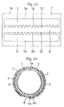
- the stage 10 While maintaining the above conditions, as shown in Figure 17, the stage 10 is moved in the direction M, and is then moved in the direction N. Because of these movements, the outer laminate 3 is wound around the outside of the outer enclosure 1, and one edge 4a is piled on the other edge 4b of the light transmitting sheet 4, as shown in Figure 14. Then, the noble gas discharge lamp is produced by adhering the edges 4a and 4b of the light transmitting sheet 4 with the adhesive layer 9.
- the noble gas discharge lamp having the above-mentioned components, light emitted from the light emitting layer 2 is concentrated in the outer enclosure 1, and is emitted from the outside of the noble gas discharge lamp via the first opening portion 7 and the aperture 2a. Therefore, when the noble gas discharge lamp is used in an office automation device such as an illumination device, the intensity of illumination on a document being scanned can be increased. As a result, accurate scanning of documents can be improved.
- the noble gas discharge lamp will have the following effects.
- the plating layer is formed between the outer electrodes 5 and 6 and the terminals 51and 61; therefore, even if the outer electrodes 5 and 6 and the terminals 51and 61 which are comprised of metals having different corrosion potential from each other, are connected directly, generation of corrosion due to the contact of different kinds of metal can be prevented.
- the width (w) of the outer electrodes 5 and 6 and the width (d) of the terminals 51and 61 are set to satisfy the following formula: 0.1 w ⁇ d ⁇ 0.5 w, generation of corrosion due to contact of different kinds of metal can be effectively prevented, in company with the existence of the plating layer. Therefore, a stable travel of electric discharge of the noble gas discharge lamp can be maintained for long periods.
- width (d) of the terminals 51and 61 is less than 0.1 w, contact intensity to the outer electrodes 5 and 6 of the terminals 51and 61 is decreased.
- width (d) of the terminals 51and 61 is more than 0.5 w, in winding the outer laminate 3 around the outside of the outer enclosure 1, the terminals 51and 61 could not be wound around the outside of the outer enclosure 1 easily . This process is extremely troublesome. Therefore, it is preferable that width (w) of the outer electrodes 5 and 6 and the width (d) of the terminals 51and 61 satisfy the above-mentioned formula.
- the adhesive layer 9 is formed on one surface of the light transmitting sheet 4; therefore, the outer laminate 3 can be adhered closely to the outside of the outer enclosure 1 by a simple step, that is, simply by rolling the outer enclosure 1 onto the outer laminate 3.
- the outer electrodes 5 and 6 are positioned previously so as to be disposed at a certain interval from each other on the light transmitting sheet 4; therefore, in adhering the outer laminate 3 to the outer enclosure 1, it is not necessary to adjust the positioning of the outer electrodes 5 and 6 to maintain a certain interval therebetween. Therefore, it can be anticipated that not only will the work efficiency be greatly improved, but automated production of the noble gas discharge lamp will also be possible. That is, production of the noble gas discharge lamp in large quantities may be anticipated.
- the resulting noble gas discharge lamp is switched on to produce light by applying a high voltage of high frequency (for example, a frequency of 30 kHz and a voltage of 2500 V o-p ) to the outer electrodes 5 and 6, from an inverter circuit 12, via the terminals 51and 61.
- a high voltage of high frequency for example, a frequency of 30 kHz and a voltage of 2500 V o-p
- the voltage applied to the outer electrodes 5 and 6 is approximately 2500 V o-p in a noble gas discharge lamp of which the outer enclosure 1 is 8 mm in external diameter and 360 mm in total length.
- this noble gas discharge lamp is different from lamps having one discharge along the longitudinal direction of the outer enclosure 1, such as a noble gas discharge lamp having a hot cathode or a cold cathode. More specifically, innumerable discharges occur between the outer electrodes 5 and 6 (discharges are generated approximately perpendicularly to the longitudinal direction of the outer enclosure 1); therefore, when such a light is turned on, light is emitted in a striped pattern in the above-mentioned noble gas discharge lamp. Electric discharges in a striped pattern cannot be confirmed under normal lighting conditions.
- the output electric power from the inverter circuit 12 is decreased 10 %, for example, by a change of voltage from a power source, the electric discharges in a striped pattern can be confirmed. Moreover, the electric discharging positions (points) are not stable and travel in the longitudinal direction of the outer enclosure 1, without interruption. The light emitting from aperture 2a is therefore intermittent.
- the noble gas discharge lamp in an illumination device for the office equipment such as facsimile machines, image-scanners, and the like, the light intensities at the points in the longitudinal direction of the aperture 2a change continuously. Therefore, it is possible that the scan accuracy of the illuminated document is extremely degraded, and the quality of reproduction may be also degraded.
- US-A-5,117,160 shows a rare gas fluorescent discharge lamp containing xenon tape as a main component and showing a pair of tape shaped Al electrodes adhered on a 0.5 mm thick outer wall of the tubular glass bulb of the lamp, an insulating silicone film being formed on the glass vessel and on the electrodes.
- the present invention provides a noble gas discharge lamp comprising of: an outer enclosure comprising a light emitting layer formed therein, and a pair of outer electrodes in the shape of a tape comprising a metal, which are adhered to the total length of the outside of the outer enclosure so as to be separated at a certain interval, and to form a first opening portion and a second opening portion, wherein the thickness of the outer enclosure is in a range of 0.2 to 0.7 mm, and at least one nonlineal edge portion is formed at at least one side portion of the outer electrodes.
- the nonlineal edge portion is formed at at least one side of the outer electrodes, in which some projections project toward the opposite electrode.
- the projections project toward the opposite electrode along the outside of the outer enclosure.
- dents are formed among the projections of the nonlineal edge portion.
- Figure 1 is a cross-sectional diagram showing the noble gas discharge lamp of the first embodiment of the present invention.
- Figure 2 is a schematic view showing the outer enclosure and outer electrodes shown in Figure 1.
- Figure 3 is a cross-sectional diagram showing the noble gas discharge lamp of the second embodiment of the present invention.
- Figure 4 is a cross-sectional diagram showing the noble gas discharge lamp of the third embodiment of the present invention.
- Figure 5 is a cross-sectional diagram showing the noble gas discharge lamp of the fourth embodiment of the present invention.
- Figure 6 is a cross-sectional diagram showing the noble gas discharge lamp of the fifth embodiment of the present invention.
- Figure 7 is a cross-sectional diagram showing the noble gas discharge lamp of the sixth embodiment of the present invention.
- Figure 8 is a schematic view showing the outer enclosure and outer electrodes used in the seventh embodiment of the present invention.
- Figure 9 is a schematic view showing the outer enclosure and outer electrodes used in the eighth embodiment of the present invention.
- Figure 10 is a schematic view showing the outer enclosure and outer electrodes used in the ninth embodiment of the present invention.
- Figure 11 is a schematic view showing the outer enclosure and outer electrodes used in the tenth embodiment of the present invention.
- Figure 12 is a schematic view showing the outer enclosure and outer electrodes used in the eleventh embodiment of the present invention.
- Figure 13 is a schematic view showing the outer enclosure and outer electrodes used in the twelfth embodiment of the present invention.
- Figure 14 is a cross-sectional diagram showing a background noble gas discharge lamp.
- Figure 15 is a schematic view showing the outer laminate shown in Figure 14.
- Figure 16 is a cross-sectional diagram taken along line X-X in Figure 15.
- Figure 17 is a schematic view showing the process for producing the noble gas discharge lamp shown in Figure 14.
- Figure 18 is a schematic view showing an electric circuit of a noble gas discharge lamp.
- the characteristic components of the noble gas discharge lamp shown in Figures 1 and 2 are as follows:
- the thickness of the outer enclosure 1A comprised of a glass bulb (tube), for example, is set in a range of 0.2 to 0.7 mm, preferably in a range of 0.4 to 0.7 mm.
- a nonlineal edge portion 5A in which triangles are formed is formed at only side portion 5b.
- the remaining portion 6b of the outer electrode 6 is formed linearly.
- the nonlineal edge portion 5A has a periodicity. More specifically, when the outer diameter of the outer enclosure 1A is 8 mm, it is preferable that the width of the outer electrode 5 including the nonlineal edge portion 5A be 8 mm, the pitch thereof be 4 mm, and the height thereof (the height of the triangle) be 1.5 mm. However, the sizes of the nonlineal edge portion 5A can be changed, depending on the situation or the object of using the noble gas discharge lamp and illumination device comprised thereof.
- the interval between the apexes of the nonlineal edge portion 5A formed at the side portion 5b and the lineal edge side portion 6b being opposite the nonlineal edge portion 5A is fixed over the entire outer electrodes 5 and 6.
- the outer enclosure 1A is comprised of materials having a large dielectric constant, reliable hermetic sealing properties, and light transmitting properties. However, it is preferable to use a lead glass having a large dielectric constant, for example.
- the thickness of the outer enclosure 1A is set in a range of 0.2 to 0.7 mm, preferably in a range of 0.4 to 0.7 mm. Excellent productivity and light properties can be obtained in this range.
- the thickness of the outer enclosure 1A is less than 0.4 mm, especially below 0. 2 mm, the mechanical strength of the outer enclosure 1A is extremely decreased. Therefore, when the outer enclosures 1A are put into commercial production, the production rate of poor quality goods (broken glass, for example) increases. In contrast, when the thickness thereof is more than 0.7 mm, electric discharges in a striped pattern can be confirmed. Moreover, light emitted from the aperture 2a becomes very intermittent. Therefore, it is preferable that the thickness of the outer enclosure 1A be in that range.
- the internal part of the outer enclosure 1A is filled with one kind of noble gas, such as xenon (Xe), krypton (Kr), neon (Ne), helium (He), and the like, or a mixture thereof.
- the outer enclosure 1A is filled with the gas under the confining pressure being in a range of 11,066 to 26,665 Pa (83 to 200 Torr).
- the confining pressure When the confining pressure is in this range, starting characteristics and light output (illumination intensity on the illuminated document) can be improved, and occurrence of intermittent illumination can be reduced. However, when the confining pressure is less than 11,066 Pa (83 Torr), light output is not sufficiently improved. In contrast, when the confining pressure is more than 26,665 Pa [200 Torr], not only are starting characteristics, inferior, but the electric discharges in a striped pattern are confirmed, and the light emitted from the aperture 2a becomes very intermittent. Therefore, it is preferable that the confining pressure of the noble gas be in that range.
- the light emitting layer 2 may include one or more kinds of fluorescent substances, depending on the manner in which the noble gas discharge lamp is to be used.
- fluorescent borates such as fluorescent europium activated yttrium ⁇ gallium borate, and the like
- fluorescent phosphate such as fluorescent cerium ⁇ terbium activated lanthanum phosphate (LaPO 4 : Ce,Tb), fluorescent tin activated strontium ⁇ magnesium phosphate ((SrMg) 3 (PO 4 ) 2 : Sn), fluorescent europium activated strontium boric phosphate (2SrO ⁇ (P 2 O 7 ⁇ B 2 O 3 ) : Eu), and the like
- fluorescent cerium ⁇ terbium activated magnesium aluminate MgAl 11 O 19 : Ce, Tb
- fluorescent cerium ⁇ terbium activated yttrium ⁇ silicate Y 2 SiO 5 : Ce, Tb
- the light emitting layer comprises a mixture of fluorescent substances, that is, fluorescent europium activated barium ⁇ magnesium aluminate having a blue emission spectrum; fluorescent cerium ⁇ terbium activated lanthanum phosphate having a green emission spectrum; and fluorescent europium activated yttrium ⁇ gallium borate having a red emission spectrum.
- the coated amount of the fluorescent substance is set in a range of 5 to 30 mg/cm 2 . In this range, the desired light output can be obtained. However, when the coated amount is less than 5 mg/cm 2 , the light output decreases; therefore, the illumination intensity on the illuminated document is insufficient. In contrast, when the coated amount is more than 30 mg/cm 2 , light emitting layer 2 having uniform quality cannot be easily obtained. Therefore, the coated amount of the fluorescent substances is preferably in this range.
- the light emitting layer 2 can be formed at a part of the inside of the outer enclosure 1A, or over the inside thereof.
- first and second opening portion 7 and 8 are formed at the interval portions between the outer electrodes 5 and 6.
- the opening angle ⁇ 1 of the first opening portion 7 is larger than the opening angle ⁇ 2 of the second opening portion 8.
- the opening angle ⁇ 1 of the first opening portion 7 be in the range of 60° to 90° , and the opening angle ⁇ 2 of the second opening portion 8 be approximately 55°.
- the opening angle ⁇ 1 of the first opening portion 7 can be outside the range, depending on the situation of using the noble gas discharge lamp.
- the second opening portion 8 be narrow so as not to cause breaks in insulation; therefore, the distance between one outer electrode 5 and the other electrode 6 in the second opening portion 8 is preferably 2 mm or more.
- the opening angle of the aperture 2a is equivalent to the first angle ⁇ 1 of the first opening portion 7, in the noble gas discharge lamp as shown in Figure 1.
- the nonlineal edge portion 5A in which some projections project toward the opposite electrode is formed at the side portion 5b. More specifically, as shown in Figure 2, the nonlineal edge portion 5A having a series of repeated triangles is formed at the side portion 5b of the outer electrode 5.
- the noble gas discharge lamp of this embodiment can be certainly lit.
- the thickness of the outer enclosure 1A is in a range of 0.2 to 0.7 mm. Therefore, in the case that the thickness of the outer enclosure 1A is at the top of this range, when a high voltage of high frequency is applied to the outer electrodes 5 and 6, intermittent illumination easily occurs, depending on the increase of voltage to the outer enclosure 1A caused by increase of resistive components. However, even if the outer enclosure 1A is at the top of that range, intermittent illumination can be effectively prevented by the thickness being in that range, in company with the existence of the nonlineal edge portion 5A at the side portion 5b of the outer electrode 5. In addition, light output from the first opening portion 7 via the aperture 2a can be effectively improved.
- the nonlineal edge portion 5A having triangles is formed at the side portion 5b from among the side portions 5b, 6b of the outer electrodes 5 and 6 which form the second portion 8; however, the side portions 5a and 6a of the outer electrodes 5 and 6 forming the first opening portion 7 are formed linearly (this shape does not influence light emission). Therefore, even when the noble gas discharge lamps are used in an illumination device, illumination of a document can be approximately uniform without further measures being taken. As a result, the precision of scanning of an illuminated document can be improved by simple components.
- the confining pressure of noble gas when the confining pressure of noble gas is high, light output increases, but the starting characteristics of the noble gas discharge lamp are degraded.
- the confining pressure of the noble gas is set to 26,665 Pa (200 Torr), starting characteristics of a practical level can be obtained by forming the nonlineal edge portion 5A in triangles at the side portion 5b of the outer electrode 5.
- occurrence of intermittent illumination is effectively prevented, and the light output can be improved. Therefore, when the noble gas discharge lamp of this embodiment is used in an illumination device, stable travel of electric discharge can be obtained, and the illumination intensity on the illuminated document can be increased; therefore, the precision of scanning of an illuminated document can be improved.
- the coated amount of the fluorescent substance is in a range of 5 to 30 mg/cm 2 ; the light output from the first opening portion 7 via the aperture 2a can be effectively improved by setting the thickness of the outer enclosure 1A to a range of 0.2 to 0.7 mm, in company with setting the confining pressure of noble gas in a range of 11,066 to 26,665 Pa (83 to 200 Torr).
- the above-mentioned range of the coated amount of the fluorescent substances is 2 to 10 times as much as the amount of the fluorescent substances employed in ordinary fluorescent lamps for illumination. It is believed that the coated amount is not preferable for ordinary fluorescent lamps for illumination. However, the light output is effectively increased in the noble gas discharge lamp of the embodiment. A cause of this phenomena is not clear; however, it may be believed that this phenomena is characteristic of a noble gas discharge lamp in which innumerable discharges are formed between the outer electrodes 5 and 6 (approximately perpendicular to the longitudinal direction of the outer enclosure 1A); therefore, a striped pattern is produced.
- the shapes of the outer electrodes 5 and 6 is formed as described above, and the coated amount of the fluorescent substances and the confining pressure of the noble gas are preferably set in those ranges, in addition to set the opening angle ⁇ 1 of the first opening portion 7 in a range of 60 to 90°, the light output emitted from the first opening portion 7 can be effectively increased.
- the leakage of light from the second portion 8 is prevented, and light output emitted from the first opening portion 7 can be more effectively increased by setting the size of the second portion 8, that is, the interval between the peak of the nonlineal edge portion 5A and the side portion 6b, to approximately 2 mm.
- FIG 3 shows the second embodiment of the present invention, and the basic components of the noble gas discharge lamp shown in Figure 3 are the same as those of the noble gas discharge lamp shown in Figure1.
- the opening angle ⁇ 3 of the aperture 2a formed in the inside of the outer enclosure 1A at the position corresponding to the first opening portion 7, is larger than the opening angle ⁇ 1 of the first opening portion 7.
- the opening angle ⁇ 3 of the aperture 2a is set in a range of 70° to 110° , for example; however, the angle ⁇ 3 can be changed depending on the situation or the object of using the noble gas discharge lamp.
- the opening angle ⁇ 1 of the first opening portion 7 and the opening angle ⁇ 2 of the second opening portion 8 satisfy the relationship of ⁇ 1 > ⁇ 2 ; however, they may be set to satisfy the relationship of ⁇ 1 ⁇ ⁇ 2 in this embodiment.
- FIG 4 shows the third embodiment of the present invention, and the basic components of the noble gas discharge lamp shown in Figure 4 are the same as those of the noble gas discharge lamp shown in Figure 1.
- One edge 4a and the outer edge 4b of the light transmitting sheet 4 are laminated to each other on the outer electrode 5, and they are melted and adhered by ultrasonic waves.
- the laminated portions 4a and 4b are melted and adhered by ultrasonic waves on the outside of the outer electrode 5; therefore, an oscillation of ultrasonic waves applying the light emitting layer 2 positioning inside of the outer electrode 1A is relieved.
- the oscillation of ultrasonic waves applying the light emitting layer 2 positioning inside of the outer electrode 1A is relieved. As a result, a peeling off of the light emitting layer 2 from the inside of the outer enclosure 1A is substantially prevented, and light output can be improved.
- the laminated portions 4a and 4b of the light transmitting sheet 4 are melted and adhered by ultrasonic waves; however, adhesion by an adhesive agent, by heat, or simultaneous use of both may also be employed.
- FIG 5 shows the fourth embodiment of the present invention, and the basic components of the noble gas discharge lamp shown in Figure 5 are the same as those of the noble gas discharge lamp shown in Figure 1.
- a pair of the outer electrodes 5 and 6 is adhered to the outside of the outer enclosure 1A by using the adhesive layer; then a light transmitting sheet 4A comprising PET resin and the like, for example, is wound and adhered on the outside of the outer enclosure 1A so as to cover the outer electrodes 5 and 6.
- the insulating ability between the outer electrodes 5 and 6 can be improved by forming an insulating coating having light transmitting properties, which is comprised of silicon varnish and the like, to the outside of the outer enclosure 1A, before winding the light transmitting sheet 4A onto the outside of the outer enclosure 1A.
- FIG 6 shows the fifth embodiment of the present invention, and the basic components of the noble gas discharge lamp shown in Figure 6 are the same as those of the noble gas discharge lamp shown in Figure 1.
- a protective tube 13 comprising thermal shrinking resin, such as PET resin and the like, is covered thereon and shrunk with heat so that the outer electrodes 5 and 6 are covered with the protective tube 13.
- the protective tube 13 can be forcibly contacted to the outside of the outer enclosure 1A by heating them to approximately 150 to 200°C, and the protective tube 13 is made to shrink by heat.
- manufacturing and working efficiency in this embodiment are not as good.
- the adhesive layer is not used, erosion does not occur due to the reaction between the material comprising the terminals 51and 61 and the adhesive composition comprising the adhesive layer. Therefore, stable travel conditions in the noble gas discharge lamp can be maintained for long periods.
- the joint portion is not formed in the protective tube 13; therefore, the peeling off of a laminated portions of the protective tube 13 can be prevented, as the light transmitting sheet 4 and 4A in the aforementioned embodiments.
- the insulating ability between the outer electrodes 5 and 6 can be improved more effectively by forming an insulating coating having light transmitting properties, which is comprised of silicon varnish and the like, to the outside of the outer enclosure 1A, before covering the protective tube 13 over the outside of the outer enclosure 1A.
- FIG 7 shows the sixth embodiment of the present invention, and the basic components of the noble gas discharge lamp shown in Figure 7 are the same as those of the noble gas discharge lamp shown in Figure 1.
- the protective tube 13 After fitting a protective tube 13 over the outside of the outer laminate 3, which is comprised of thermal shrinking resins, such as PET resin, and the like, the protective tube 13 is made to shrink with heat.
- the protective tube 13 can be contacted forcibly to the outside of the light transmitting sheet 4 by heating them to approximately 150°C to 200°C, and the protective tube 13 is made to shrink by heat.
- the characteristic structure of this embodiment can be applied to the noble gas discharge lamps shown in Figures 3 to 6.
- the light transmitting sheet 4 and 4A and the protective tube 13 may be omitted in these embodiments.
- the nonlineal edge portion is formed at at least one side of a pair of the outer electrodes, in which some projections project toward the opposite electrode.
- the nonlineal edge portions shown in Figures 8 to 13 are preferable.
- Figure 8 shows the seventh embodiment of the present invention, and shows unfolding of outer enclosure 1A.
- the basic components of the noble gas discharge lamp shown in Figure 8 are the same as those of the noble gas discharge lamp shown in Figure 1.
- the nonlineal edge portions 5A and 6A are formed at the side portions 5a, 5b, 6a, and 6b of a pair of the outer electrode 5 and 6 which have a tape shape and are positioned at the outside of the outer enclosure 1A. Moreover, the nonlineal edge portions 5A and 6A, that is, the side portions 5a, 5b, 6a, and 6b form the first and second opening portions 7 and 8. The nonlineal edge portions 5A and 6A are in a series of repeated triangles.
- the interval between the peaks of the nonlineal edge portions 5A and 6A is fixed along the longitudinal direction of the outer electrodes 5 and 6.
- the nonlineal edge portions 5A and 6A are formed at all side portions 5a, 5b, 6a, and 6b of the outer electrodes 5 and 6; therefore, when a high voltage of high frequency is applied to the noble gas discharge lamp of this embodiment, the electrical field is remarkably concentrated at the peaks of the nonlineal edge portions 5A and 6A, and the starting characteristics thereof can be improved. In particular, when the peaks of the nonlineal edge portions 5A and 6A correspond to each other, the starting characteristics thereof can be effectively improved.
- Figure 9 shows the eighth embodiment of the present invention, and shows unfolding of outer enclosure 1A.
- the basic components of the noble gas discharge lamp shown in Figure 9 are the same as those of the noble gas discharge lamp shown in Figure 1.
- the nonlineal edge portions 5A and 6A are formed at the side portions 5b and 6b (they form the second opening portion 8) of a pair of the outer electrodes 5 and 6 having a tape shape which are positioned at the outside of the outer enclosure 1A.
- the nonlineal edge portions 5A and 6A are in a series of repeated triangles.
- the side portions 5a and 6a forming the first opening portion 7 are formed linearly.
- the side portions 5a and 6a forming the first opening portion 7 are formed linearly; therefore, illumination on the document can be approximately uniform. As a result, the precision of scanning of an illuminated document can be improved.
- Figure 10 shows the ninth embodiment of the present invention, and shows unfolding of outer enclosure 1A.
- the basic components of the noble gas discharge lamp shown in Figure 10 are the same as those of the noble gas discharge lamp shown in Figure 1.
- the nonlineal edge portion 5B is formed at only side portion 5b from among the side portions 5b and 6b forming the second opening portion 8.
- the nonlineal edge portion 5B is in a wave shape, for example, a series of repeated semicircles.
- the side portion 6b being opposite to the side portion 5b, that is, the nonlineal edge portion 5B, is formed linearly.
- Figure 11 shows the tenth embodiment of the present invention, and shows unfolding of outer enclosure 1A.
- the basic components of the noble gas discharge lamp shown in Figure 11 are the same as those of the noble gas discharge lamp shown in Figure 1.
- the nonlineal edge portions 5B and 6B are formed at the side portions 5b and 6b (they form the second opening portion 8) of a pair of the outer electrodes 5 and 6.
- the nonlineal edge portions 5A and 6A are in a wave shape, for example, a series of repeated semicircles.
- the side portions 5a and 6a forming the first opening portion 7 are formed linearly.
- nonlineal edge portions 5B and 6B may be formed at all side portions 5a, 5b, 6a, and 6b. That is, all the side portions 5a, 5b, 6a, and 6b, may be formed in a series of repeated semicircle.
- Figure 12 shows the eleventh embodiment of the present invention, and shows unfolding of outer enclosure 1A
- the basic components of the noble gas discharge lamp shown in Figure 12 are the same as those of the noble gas discharge lamp shown in Figure 1.
- the nonlineal edge portion 5C is formed at only the side portion 5b from among side portions 5b and 6b forming the second opening portion 8.
- the nonlineal edge portion 5C is in a series of repeated polygons, such as rectangles and trapezoids.
- the side portion 6b being opposite to the side portion 5b is formed linearly.
- the remaining side portions 5a, 6a, and 6b of the outer electrodes 5 and 6 beside the side portion 5b of the outer electrode 5 are formed linearly.
- Figure 13 shows the twelfth embodiment of the present invention, and shows unfolding of outer enclosure 1A.
- the basic components of the noble gas discharge lamp shown in Figure 13 are the same as those of the noble gas discharge lamp shown in Figure 1.
- the nonlineal edge portions 5C and 6C are formed at the side portions 5b and 6b forming the second opening portion 8.
- the nonlineal edge portions 5C and 6C are in a series of repeated polygons, specifically, rectangles.
- the side portions 5a and 6a forming the first opening portion 7 are formed linearly.
- nonlineal edge portions 5C and 6C may be formed at all side portions 5a, 5b, 6a, and 6b. That is, all side portions 5a, 5b, 6a, and 6b may be formed in a series of repeated polygons, such as rectangles.
- At least one of the outer electrodes 5 and 6 having the above-mentioned nonlineal edge portion 5A, 5B, 5C, 6A, 6B and 6C can be applied to the noble gas discharge lamps shown in Figures 1 to 7 in suitable combinations.
- the pitch and the height of the nonlineal edge portions 5A, 5B, 5C, 6A, 6B and 6C can be modified, depending on the size of the noble gas discharge lamp.
- the fluorescent water-soluble coating solution containing fluorescent cerium ⁇ terbium activated yttrium ⁇ silicate (Y 2 SiO 5 : Ce, Tb) having an emission spectrum in yellow-green wavelengths was obtained.
- the light emitting layer 2 was formed by coating the obtained fluorescent water-soluble coating solution on the inside of the outer enclosure 1A comprised of lead glass, which was 8 mm in external diameter, 0.5 mm in thickness, and 360 mm in length. Moreover, the coating amount of the fluorescent water-soluble coating solution was 15 mg/cm 2 .
- the aperture 2a having 75° in the opening angle ⁇ 3 was obtained by forcibly peeling off a part of the obtained light emitting layer 2 using a scraper.
- the outer enclosure 1A was sealed, and filled with xenon gas at a confining pressure being varied in a range of 9,333 to 30,664 Pa (70 to 230 Torr).
- the noble gas discharge lamps of this Experimental Example were produced by the same steps shown in Figures 17. Moreover, a pair of the outer electrodes 5 and 6 was comprised of aluminum foil in the shape of a tape 8 mm in width. As shown in Figure 2, the nonlineal edge portion 5A was formed at only one side portion 5b of the outer electrode 5 forming the second opening portion 8, in which triangles 4 mm in pitch and 1.5 mm in peak height were formed.
- the confining pressure of xenon gas is 26,665 Pa (200 Torr) or less, even when the output voltage (frequency fixed at 30 kHz) of the inverter circuit 12 was set to 90 % of a fixed voltage (2500 V o-p ), the intermittent illumination cannot be confirmed, and stable travel of electric discharge can be obtained after the lamps are lit.
- the starting voltage in a range of 300 to 600 V can be decreased in the noble gas discharge lamps of this Experimental Example.
- the confining pressure is 11,066 Pa (83 Torr) or greater in the conventional noble gas discharge lamp, the intermittent illumination can be confirmed.
- the confining pressure reaches 13,332 Pa (100 Torr)
- the conventional noble gas discharge lamp cannot be used in practice without difficulty.
- the lamps can be lit with a fixed voltage (2500 V o-p ); however, start-up is not assured when the input power was decreased.
- the obtained noble gas discharge lamps were incorporated in an electric circuit as shown in Figure 18, and the output voltage (frequency fixed at 30 kHz) of the inverter circuit 12 was set to 90 % of a fixed voltage (2500 V o-p ). In these conditions, the illumination intensities on the document were measured at a point 8 mm away from the outer enclosure 1. The results were shown in the following Table 2.
- the obtained noble gas discharge lamps were incorporated in an electric circuit as shown in Figure 18, and the output voltage (frequency fixed at 30 kHz) of the inverter circuit 12 was set to 90 % of a fixed voltage (2500 V o-p ). In these conditions, the occurrence of intermittent illumination was evaluated at a point 8 mm away from the outer enclosure. The results were shown in the following Table 2.
- the confining pressure of xenon gas is 19,998 Pa (150 Torr) or less, a stable travel of electric discharge without occurrence of intermittent illumination can be obtained.
- the confining pressure of xenon gas is 26,665 Pa (200 Torr)
- some intermittent illumination did occur, but the noble gas discharge lamp can be used in practice without difficulty.
- the confining pressure being more than 26,665 Pa (200 Torr), specifically 27,998 Pa (210 Torr) and 30,664 Pa (230 Torr), the significant intermittent illumination occurs, and it is confirmed that it is difficult to use the noble gas discharge lamps in an illumination device.
- the illumination intensity on the illuminated document increases, depending on an increase of the confining pressure of xenon gas; however, a stable illumination intensity without occurrence of intermittent illumination can be obtained when the confining pressure of xenon gas is in a range of 26,665 Pa (200 Torr) or less.
- the obtained noble gas discharge lamps were incorporated in an electric circuit as shown in Figure 18, and the output voltage (frequency fixed at 30 kHz) of the inverter circuit 12 was set to 90 % of a fixed voltage (2500 V o-p ). In these conditions, the occurrence of intermittent illumination was evaluated at a point 8 mm away from the outer enclosure. The results were shown in the following Table 3.
- ⁇ means that intermittent illumination did not occur, ⁇ means that some intermittent illumination did occur, but the noble gas discharge lamp can be used in practice without difficulty, and ⁇ means that intermittent illumination did occur, and the noble gas discharge lamp cannot be used in practice without difficulty.
- ⁇ means that damage to the outer enclosure was not observed, and the strength of the outer enclosure is sufficient; ⁇ means that some damage was observed in the outer enclosure, but the noble gas discharge lamps comprising the outer enclosures were at least usable; and ⁇ means that serious damage to the outer enclosure was observed and the strength of the outer enclosure meant the produced noble gas discharge lamps would be difficult to use.
- Thickness of the outer enclosure (mm) Occurrence of intermittent illumination Strength 0.18 ⁇ ⁇ 0.2 ⁇ ⁇ 0.25 ⁇ ⁇ 0.4 ⁇ ⁇ 0.5 ⁇ ⁇ 0.6 ⁇ 0.7 ⁇ 0.8 ⁇ ⁇
- the thickness of the outer enclosure 1A is in a range of 0.18 to 0.6 mm, the occurrence of intermittent illumination cannot be confirmed, even when the output is low.
- the noble gas discharge lamp can be used in practice without difficulty.
- the thickness of the outer enclosure is preferably in a range of 0.2 to 0.7 mm, more preferably in a range of 0.4 to 0.7 mm.
Landscapes
- Physics & Mathematics (AREA)
- Electromagnetism (AREA)
- Engineering & Computer Science (AREA)
- Plasma & Fusion (AREA)
- Vessels And Coating Films For Discharge Lamps (AREA)
Claims (11)
- Edelgas-Entladungslampe mit:wobei die Dicke des Außengefäßes (1A) im Bereich von 0,2 bis 0,7 mm liegt, dadurch gekennzeichnet, dasseinem Außengefäß (1A) mit einer darin ausgebildeten Licht emittierenden Schicht (2) und einem Paar Außenelektroden (5, 6) in Bandform, die ein Metall aufweisen, die an der gesamten Länge der Außenseite des Außengefäßes (1A) so angebracht sind, dass eine Außenelektrode (5) und die andere Außenelektrode (6) in einem gewissen Abstand voneinander getrennt sind, und einen ersten Öffnungsteil (7) und einen zweiten Öffnungsteil (8) bilden;
wenigstens ein nicht linearer Kantenteil (5A, 5B, 5C, 6A, 6B, 6C) an welchem einige Vorsprünge in Richtung auf die gegenüberliegende Elektrode vorstehen, an wenigstens einem Seitenteil (5a, 5b, 6a, 6b) der Außenelektroden (5, 6) ausgebildet ist, und dass zwischen den Vorsprüngen der nicht linearen Kantenteile (5A, 5B, 5C, 6A, 6B, 6C) Zähne ausgebildet sind. - Edelgas-Entladungslampe nach Anspruch 1, wobei von der Licht emittierenden Schicht (2) emittiertes Licht hauptsächlich von dem ersten Öffhungsteil (7) emittiert wird, und an wenigstens einem Seitenteil (5b, 6b) des Paares Außenelektroden (5, 6), die den zweiten Öffnungsteil (8) bilden, wenigstens ein nicht linearer Kantenteil (5A, 5B, 5C, 6A, 6B, 6C), an welchem einige Vorsprünge zur gegenüberliegenden Elektrode vorstehen, ausgebildet ist.
- Edelgas-Entladungslampe nach Anspruch 2, wobei die Außenseite des Außengefäßes (1A) mit einem Isoliermaterial beschichtet ist, um die Außenelektroden (5, 6) abzudecken.
- Edelgas-Entladungslampe nach Anspruch 3, wobei das Isoliermaterial wenigstens ein Material ist, das aus der Gruppe ausgewählt ist, die besteht aus einem Schutzrohr (13), das ein wärmeschrumpfendes Kunstharz enthält, und einer lichtdurchlässigen Folie (4, 4A).
- Edelgas-Entladungslampe nach Anspruch 1, wobei die Edelgas-Entladungslampe das Außengefäß (1A) in Form eines geraden Rohres und eines Außenlaminates (3) aufweist,
wobei das Außenlaminat (3) eine lichtdurchlässige Folie (4, 4A), die Außenelektroden (5, 6) und eine Klebstoffschicht (9) enthält,
die lichtdurchlässige Folie (4, 4A) die gleiche Länge wie das Außengefäß (1A) hat,
das Paar Außenelektroden (5, 6) die Form von Bändern hat, die ein Metall aufweisen, welche an einer Oberfläche der lichtdurchlässigen Folie (4, 4A) so positioniert sind, dass die Außenelektrode (5) und die Außenelektrode (6) voneinander getrennt sind, und
die Klebstoffschicht (9) an der Oberfläche der lichtdurchlässigen Folie (4, 4A) ausgebildet ist, auf welcher die Außenelektroden (5, 6) positioniert sind,
wobei die Klebstoffschicht 9 zwischen dem Paar Außenelektroden (5, 6) und dem Außengefäß (1A) ausgebildet ist, und die lichtdurchlässige Folie (4, 4A), die die gleiche Länge wie das Außengefäß (1A) hat, um die Außenseite des Außengefäßes (1A) gewickelt und an diese angeklebt ist, sodass die Außenelektroden (5 und 6) abgedeckt sind. - Edelgas-Entladungslampe nach Anspruch 1, wobei der wenigstens eine nicht lineare Kantenteil (5A, 5B, 5C, 6A, 6B, 6C), an welchem einige Vorsprünge in Richtung auf die gegenüberliegende Elektrode vorstehen, über die gesamte Länge der Außenelektrode (5, 6) ausgebildet ist.
- Edelgas-Entladungslampe nach Anspruch 6, wobei der nicht lineare Kantenteil (5A, 5B, 5C, 6A, 6B, 6C), an dem einige Vorsprünge in Richtung auf die gegenüberliegende Elektrode vorstehen, in einer Reihe von sich wiederholenden Formen ausgebildet ist, wobei die Formen wenigstens eine Form aus der Gruppe aufweisen, bestehend aus einer Dreiecks-, einer Polygon- und einer Wellenform.
- Edelgas-Entladungslampe nach Anspruch 7, wobei das Polygon trapezoidförmig ist.
- Edelgas-Entladungslampe nach Anspruch 7, wobei die Wellenform eine Reihe von sich wiederholenden Halbkreisen ist.
- Edelgas-Entladungslampe nach Anspruch 1, wobei eine Öffnung (2a) an der Innenseite des Außengefäßes (1A) an einer Position korrespondierend zu dem ersten Öffnungsteil (7), ausgebildet ist, an welcher die Licht emittierenden Schicht (2) nicht ausgebildet ist.
- Edelgas-Entladungslampe nach Anspruch 1, wobei das Außengefäß (1A) mit Xenongas gefüllt ist.
Applications Claiming Priority (3)
| Application Number | Priority Date | Filing Date | Title |
|---|---|---|---|
| JP08839897A JP3635850B2 (ja) | 1997-04-07 | 1997-04-07 | 希ガス放電灯 |
| JP88398/97 | 1997-04-07 | ||
| JP8839897 | 1997-04-07 |
Publications (2)
| Publication Number | Publication Date |
|---|---|
| EP0871205A1 EP0871205A1 (de) | 1998-10-14 |
| EP0871205B1 true EP0871205B1 (de) | 2003-03-12 |
Family
ID=13941696
Family Applications (1)
| Application Number | Title | Priority Date | Filing Date |
|---|---|---|---|
| EP98106166A Expired - Lifetime EP0871205B1 (de) | 1997-04-07 | 1998-04-03 | Edelgasentladungslampe |
Country Status (4)
| Country | Link |
|---|---|
| US (1) | US6034476A (de) |
| EP (1) | EP0871205B1 (de) |
| JP (1) | JP3635850B2 (de) |
| DE (1) | DE69811974T2 (de) |
Cited By (1)
| Publication number | Priority date | Publication date | Assignee | Title |
|---|---|---|---|---|
| EP1536453A3 (de) * | 2003-10-09 | 2007-08-08 | Patent-Treuhand-Gesellschaft für elektrische Glühlampen mbH | Entladungslampe mit mindestens einer aussenelektrode und Verfahren zu ihrer Herstellung |
Families Citing this family (12)
| Publication number | Priority date | Publication date | Assignee | Title |
|---|---|---|---|---|
| US6347480B1 (en) * | 1997-07-07 | 2002-02-19 | Southpac Trust International, Inc. | Method for wrapping a floral grouping with a sheet of material constructed of paper and having printed and embossed patterns thereon |
| ZA9711281B (en) * | 1996-12-20 | 1998-09-21 | Fusion Lighting Inc | High efficiency electrodeless lamp apparatus with frit sealed ceramic reflecting housing that contains a plasma light source |
| JPH10289693A (ja) * | 1997-04-11 | 1998-10-27 | Nec Home Electron Ltd | 希ガス放電灯 |
| TW381294B (en) | 1997-05-20 | 2000-02-01 | Fusion Lighting Inc | Lamp bulb with integral reflector |
| TW558732B (en) | 2001-09-19 | 2003-10-21 | Matsushita Electric Industrial Co Ltd | Light source apparatus and liquid crystal display apparatus using the same |
| US6891334B2 (en) * | 2001-09-19 | 2005-05-10 | Matsushita Electric Industrial Co., Ltd. | Light source device and liquid crystal display employing the same |
| US6806648B2 (en) * | 2001-11-22 | 2004-10-19 | Matsushita Electric Industrial Co., Ltd. | Light source device and liquid crystal display device |
| US6906461B2 (en) * | 2001-12-28 | 2005-06-14 | Matsushita Electric Industrial Co., Ltd. | Light source device with inner and outer electrodes and liquid crystal display device |
| JP3889987B2 (ja) * | 2002-04-19 | 2007-03-07 | パナソニック フォト・ライティング 株式会社 | 放電灯装置及びバックライト |
| KR101079574B1 (ko) | 2007-01-15 | 2011-11-03 | 삼성전자주식회사 | 조명광원 및 이를 채용한 스캐너 모듈 및 이미지스캐닝장치 |
| DE112007003399A5 (de) * | 2007-04-27 | 2010-08-05 | Osram Gesellschaft mit beschränkter Haftung | Dielektrische Barrieren-Entladungslampe in Doppelrohrkonfiguration |
| TWI382446B (zh) * | 2007-10-09 | 2013-01-11 | Ushio Electric Inc | Double tube type rare gas fluorescent lamp |
Family Cites Families (5)
| Publication number | Priority date | Publication date | Assignee | Title |
|---|---|---|---|---|
| US5117160C1 (en) * | 1989-06-23 | 2001-07-31 | Nec Corp | Rare gas discharge lamp |
| DE69210113T2 (de) * | 1991-07-01 | 1996-11-21 | Philips Patentverwaltung | Hochdrucksglimmentladungslampe |
| JP3075041B2 (ja) * | 1992-12-28 | 2000-08-07 | 三菱電機株式会社 | ガス放電表示装置 |
| JPH06314561A (ja) * | 1993-05-06 | 1994-11-08 | Mitsubishi Electric Corp | 放電ランプ |
| JP3218561B2 (ja) * | 1997-06-27 | 2001-10-15 | スタンレー電気株式会社 | 蛍光ランプ |
-
1997
- 1997-04-07 JP JP08839897A patent/JP3635850B2/ja not_active Expired - Fee Related
-
1998
- 1998-04-03 US US09/054,908 patent/US6034476A/en not_active Expired - Lifetime
- 1998-04-03 DE DE69811974T patent/DE69811974T2/de not_active Expired - Lifetime
- 1998-04-03 EP EP98106166A patent/EP0871205B1/de not_active Expired - Lifetime
Cited By (2)
| Publication number | Priority date | Publication date | Assignee | Title |
|---|---|---|---|---|
| EP1536453A3 (de) * | 2003-10-09 | 2007-08-08 | Patent-Treuhand-Gesellschaft für elektrische Glühlampen mbH | Entladungslampe mit mindestens einer aussenelektrode und Verfahren zu ihrer Herstellung |
| US7298071B2 (en) | 2003-10-09 | 2007-11-20 | Patent - Treuhand - Gesellschaft Fuer Elektrische Gluehlampen Mbh | Discharge lamp having at least one external electrode, adhesive layer, and carrier film |
Also Published As
| Publication number | Publication date |
|---|---|
| DE69811974D1 (de) | 2003-04-17 |
| JPH10284009A (ja) | 1998-10-23 |
| US6034476A (en) | 2000-03-07 |
| JP3635850B2 (ja) | 2005-04-06 |
| EP0871205A1 (de) | 1998-10-14 |
| DE69811974T2 (de) | 2003-12-24 |
Similar Documents
| Publication | Publication Date | Title |
|---|---|---|
| EP0871205B1 (de) | Edelgasentladungslampe | |
| KR100977907B1 (ko) | 형광램프, 백라이트 유닛, 및 액정표시장치 | |
| EP0871204B1 (de) | Edelgasentladungslampe | |
| US6150758A (en) | Noble gas discharge lamp having external electrodes with first and second openings and a specified amount of fluorescent coating material | |
| EP0871203A2 (de) | Edelgas-Entladungslampe | |
| JP2008218403A (ja) | 放電ランプ、バックライトユニット、および液晶表示装置 | |
| JPH1186797A (ja) | 希ガス放電灯 | |
| JP3025216B2 (ja) | 希ガス放電灯 | |
| JP3032802B2 (ja) | 希ガス放電灯 | |
| JP3635864B2 (ja) | 希ガス放電灯 | |
| JPH11167901A (ja) | 希ガス放電灯及びその製造方法 | |
| JP3684721B2 (ja) | 希ガス放電灯 | |
| JP3965775B2 (ja) | 希ガス放電灯 | |
| JP3959838B2 (ja) | 希ガス放電灯 | |
| JP3921810B2 (ja) | 希ガス放電灯 | |
| JP3678581B2 (ja) | 希ガス放電灯 | |
| JP3921804B2 (ja) | 希ガス放電灯 | |
| KR20080088361A (ko) | 방전 램프 | |
| KR20070009425A (ko) | 외부 전극을 구비한 방전램프 및 그 제조방법, 당해방전램프를 구비한 백라이트 유닛 및 액정표시장치 | |
| JP3624594B2 (ja) | アパーチャ形希ガス放電灯 | |
| JPH1186798A (ja) | 希ガス放電灯 | |
| JPH11144688A (ja) | 希ガス放電灯 | |
| JPH11144886A (ja) | 希ガス放電灯の点灯装置 | |
| JPH10162783A (ja) | アパ−チャ形希ガス放電灯及びその製造方法 | |
| JPH118086A (ja) | 希ガス放電灯 |
Legal Events
| Date | Code | Title | Description |
|---|---|---|---|
| PUAI | Public reference made under article 153(3) epc to a published international application that has entered the european phase |
Free format text: ORIGINAL CODE: 0009012 |
|
| 17P | Request for examination filed |
Effective date: 19980715 |
|
| AK | Designated contracting states |
Kind code of ref document: A1 Designated state(s): DE FR GB |
|
| AX | Request for extension of the european patent |
Free format text: AL;LT;LV;MK;RO;SI |
|
| AKX | Designation fees paid |
Free format text: DE FR GB |
|
| 17Q | First examination report despatched |
Effective date: 20000317 |
|
| GRAG | Despatch of communication of intention to grant |
Free format text: ORIGINAL CODE: EPIDOS AGRA |
|
| GRAG | Despatch of communication of intention to grant |
Free format text: ORIGINAL CODE: EPIDOS AGRA |
|
| GRAH | Despatch of communication of intention to grant a patent |
Free format text: ORIGINAL CODE: EPIDOS IGRA |
|
| RAP1 | Party data changed (applicant data changed or rights of an application transferred) |
Owner name: USHIODENKI KABUSHIKI KAISHA |
|
| RAP1 | Party data changed (applicant data changed or rights of an application transferred) |
Owner name: USHIODENKI KABUSHIKI KAISHA Owner name: NEC CORPORATION |
|
| GRAH | Despatch of communication of intention to grant a patent |
Free format text: ORIGINAL CODE: EPIDOS IGRA |
|
| GRAA | (expected) grant |
Free format text: ORIGINAL CODE: 0009210 |
|
| AK | Designated contracting states |
Designated state(s): DE FR GB |
|
| REG | Reference to a national code |
Ref country code: GB Ref legal event code: FG4D |
|
| REF | Corresponds to: |
Ref document number: 69811974 Country of ref document: DE Date of ref document: 20030417 Kind code of ref document: P |
|
| ET | Fr: translation filed | ||
| PLBE | No opposition filed within time limit |
Free format text: ORIGINAL CODE: 0009261 |
|
| STAA | Information on the status of an ep patent application or granted ep patent |
Free format text: STATUS: NO OPPOSITION FILED WITHIN TIME LIMIT |
|
| 26N | No opposition filed |
Effective date: 20031215 |
|
| REG | Reference to a national code |
Ref country code: FR Ref legal event code: PLFP Year of fee payment: 19 |
|
| PGFP | Annual fee paid to national office [announced via postgrant information from national office to epo] |
Ref country code: FR Payment date: 20160309 Year of fee payment: 19 Ref country code: GB Payment date: 20160330 Year of fee payment: 19 |
|
| PGFP | Annual fee paid to national office [announced via postgrant information from national office to epo] |
Ref country code: DE Payment date: 20160330 Year of fee payment: 19 |
|
| REG | Reference to a national code |
Ref country code: DE Ref legal event code: R119 Ref document number: 69811974 Country of ref document: DE |
|
| GBPC | Gb: european patent ceased through non-payment of renewal fee |
Effective date: 20170403 |
|
| REG | Reference to a national code |
Ref country code: FR Ref legal event code: ST Effective date: 20171229 |
|
| PG25 | Lapsed in a contracting state [announced via postgrant information from national office to epo] |
Ref country code: DE Free format text: LAPSE BECAUSE OF NON-PAYMENT OF DUE FEES Effective date: 20171103 Ref country code: FR Free format text: LAPSE BECAUSE OF NON-PAYMENT OF DUE FEES Effective date: 20170502 |
|
| PG25 | Lapsed in a contracting state [announced via postgrant information from national office to epo] |
Ref country code: GB Free format text: LAPSE BECAUSE OF NON-PAYMENT OF DUE FEES Effective date: 20170403 |