EP0860101B1 - Verfahren zur herstellung von kontaktlöchern auf adapterplatten und adapterplatte zur prüfung von musterplatten - Google Patents
Verfahren zur herstellung von kontaktlöchern auf adapterplatten und adapterplatte zur prüfung von musterplatten Download PDFInfo
- Publication number
- EP0860101B1 EP0860101B1 EP96938583A EP96938583A EP0860101B1 EP 0860101 B1 EP0860101 B1 EP 0860101B1 EP 96938583 A EP96938583 A EP 96938583A EP 96938583 A EP96938583 A EP 96938583A EP 0860101 B1 EP0860101 B1 EP 0860101B1
- Authority
- EP
- European Patent Office
- Prior art keywords
- contact pads
- contact
- board
- adapter
- electrically conducting
- Prior art date
- Legal status (The legal status is an assumption and is not a legal conclusion. Google has not performed a legal analysis and makes no representation as to the accuracy of the status listed.)
- Expired - Lifetime
Links
- 238000004519 manufacturing process Methods 0.000 title claims abstract description 8
- 238000012360 testing method Methods 0.000 title claims description 21
- 238000005530 etching Methods 0.000 claims abstract description 24
- 238000007747 plating Methods 0.000 claims abstract description 18
- 239000004020 conductor Substances 0.000 claims abstract description 15
- 238000000034 method Methods 0.000 claims description 4
- 239000000463 material Substances 0.000 abstract description 8
- 230000001681 protective effect Effects 0.000 description 12
- 229920001971 elastomer Polymers 0.000 description 5
- 239000005060 rubber Substances 0.000 description 5
- RYGMFSIKBFXOCR-UHFFFAOYSA-N Copper Chemical compound [Cu] RYGMFSIKBFXOCR-UHFFFAOYSA-N 0.000 description 4
- 229910052802 copper Inorganic materials 0.000 description 4
- 239000010949 copper Substances 0.000 description 4
- 238000005520 cutting process Methods 0.000 description 4
- 238000003825 pressing Methods 0.000 description 4
- ATJFFYVFTNAWJD-UHFFFAOYSA-N Tin Chemical compound [Sn] ATJFFYVFTNAWJD-UHFFFAOYSA-N 0.000 description 2
- 238000009826 distribution Methods 0.000 description 2
- 239000007858 starting material Substances 0.000 description 2
- 239000003795 chemical substances by application Substances 0.000 description 1
- 239000000470 constituent Substances 0.000 description 1
- 230000008878 coupling Effects 0.000 description 1
- 238000010168 coupling process Methods 0.000 description 1
- 238000005859 coupling reaction Methods 0.000 description 1
- 230000001419 dependent effect Effects 0.000 description 1
- 239000012777 electrically insulating material Substances 0.000 description 1
- 239000002184 metal Substances 0.000 description 1
- 229910052751 metal Inorganic materials 0.000 description 1
- 229920003052 natural elastomer Polymers 0.000 description 1
- 229920001194 natural rubber Polymers 0.000 description 1
- 239000004033 plastic Substances 0.000 description 1
- 229920003023 plastic Polymers 0.000 description 1
- 229920003051 synthetic elastomer Polymers 0.000 description 1
- 239000005061 synthetic rubber Substances 0.000 description 1
- 238000012876 topography Methods 0.000 description 1
Images


Classifications
-
- H—ELECTRICITY
- H05—ELECTRIC TECHNIQUES NOT OTHERWISE PROVIDED FOR
- H05K—PRINTED CIRCUITS; CASINGS OR CONSTRUCTIONAL DETAILS OF ELECTRIC APPARATUS; MANUFACTURE OF ASSEMBLAGES OF ELECTRICAL COMPONENTS
- H05K3/00—Apparatus or processes for manufacturing printed circuits
- H05K3/40—Forming printed elements for providing electric connections to or between printed circuits
- H05K3/4007—Surface contacts, e.g. bumps
-
- G—PHYSICS
- G01—MEASURING; TESTING
- G01R—MEASURING ELECTRIC VARIABLES; MEASURING MAGNETIC VARIABLES
- G01R1/00—Details of instruments or arrangements of the types included in groups G01R5/00 - G01R13/00 and G01R31/00
- G01R1/02—General constructional details
- G01R1/06—Measuring leads; Measuring probes
- G01R1/067—Measuring probes
- G01R1/073—Multiple probes
- G01R1/07307—Multiple probes with individual probe elements, e.g. needles, cantilever beams or bump contacts, fixed in relation to each other, e.g. bed of nails fixture or probe card
- G01R1/07364—Multiple probes with individual probe elements, e.g. needles, cantilever beams or bump contacts, fixed in relation to each other, e.g. bed of nails fixture or probe card with provisions for altering position, number or connection of probe tips; Adapting to differences in pitch
- G01R1/07378—Multiple probes with individual probe elements, e.g. needles, cantilever beams or bump contacts, fixed in relation to each other, e.g. bed of nails fixture or probe card with provisions for altering position, number or connection of probe tips; Adapting to differences in pitch using an intermediate adapter, e.g. space transformers
-
- H—ELECTRICITY
- H05—ELECTRIC TECHNIQUES NOT OTHERWISE PROVIDED FOR
- H05K—PRINTED CIRCUITS; CASINGS OR CONSTRUCTIONAL DETAILS OF ELECTRIC APPARATUS; MANUFACTURE OF ASSEMBLAGES OF ELECTRICAL COMPONENTS
- H05K3/00—Apparatus or processes for manufacturing printed circuits
- H05K3/22—Secondary treatment of printed circuits
-
- H—ELECTRICITY
- H05—ELECTRIC TECHNIQUES NOT OTHERWISE PROVIDED FOR
- H05K—PRINTED CIRCUITS; CASINGS OR CONSTRUCTIONAL DETAILS OF ELECTRIC APPARATUS; MANUFACTURE OF ASSEMBLAGES OF ELECTRICAL COMPONENTS
- H05K2201/00—Indexing scheme relating to printed circuits covered by H05K1/00
- H05K2201/03—Conductive materials
- H05K2201/0332—Structure of the conductor
- H05K2201/0335—Layered conductors or foils
- H05K2201/0347—Overplating, e.g. for reinforcing conductors or bumps; Plating over filled vias
-
- H—ELECTRICITY
- H05—ELECTRIC TECHNIQUES NOT OTHERWISE PROVIDED FOR
- H05K—PRINTED CIRCUITS; CASINGS OR CONSTRUCTIONAL DETAILS OF ELECTRIC APPARATUS; MANUFACTURE OF ASSEMBLAGES OF ELECTRICAL COMPONENTS
- H05K2201/00—Indexing scheme relating to printed circuits covered by H05K1/00
- H05K2201/03—Conductive materials
- H05K2201/0332—Structure of the conductor
- H05K2201/0364—Conductor shape
- H05K2201/0367—Metallic bump or raised conductor not used as solder bump
-
- H—ELECTRICITY
- H05—ELECTRIC TECHNIQUES NOT OTHERWISE PROVIDED FOR
- H05K—PRINTED CIRCUITS; CASINGS OR CONSTRUCTIONAL DETAILS OF ELECTRIC APPARATUS; MANUFACTURE OF ASSEMBLAGES OF ELECTRICAL COMPONENTS
- H05K2201/00—Indexing scheme relating to printed circuits covered by H05K1/00
- H05K2201/09—Shape and layout
- H05K2201/09209—Shape and layout details of conductors
- H05K2201/09372—Pads and lands
- H05K2201/09481—Via in pad; Pad over filled via
-
- H—ELECTRICITY
- H05—ELECTRIC TECHNIQUES NOT OTHERWISE PROVIDED FOR
- H05K—PRINTED CIRCUITS; CASINGS OR CONSTRUCTIONAL DETAILS OF ELECTRIC APPARATUS; MANUFACTURE OF ASSEMBLAGES OF ELECTRICAL COMPONENTS
- H05K2201/00—Indexing scheme relating to printed circuits covered by H05K1/00
- H05K2201/09—Shape and layout
- H05K2201/09209—Shape and layout details of conductors
- H05K2201/09372—Pads and lands
- H05K2201/0949—Pad close to a hole, not surrounding the hole
-
- H—ELECTRICITY
- H05—ELECTRIC TECHNIQUES NOT OTHERWISE PROVIDED FOR
- H05K—PRINTED CIRCUITS; CASINGS OR CONSTRUCTIONAL DETAILS OF ELECTRIC APPARATUS; MANUFACTURE OF ASSEMBLAGES OF ELECTRICAL COMPONENTS
- H05K2201/00—Indexing scheme relating to printed circuits covered by H05K1/00
- H05K2201/09—Shape and layout
- H05K2201/09209—Shape and layout details of conductors
- H05K2201/09654—Shape and layout details of conductors covering at least two types of conductors provided for in H05K2201/09218 - H05K2201/095
- H05K2201/098—Special shape of the cross-section of conductors, e.g. very thick plated conductors
-
- H—ELECTRICITY
- H05—ELECTRIC TECHNIQUES NOT OTHERWISE PROVIDED FOR
- H05K—PRINTED CIRCUITS; CASINGS OR CONSTRUCTIONAL DETAILS OF ELECTRIC APPARATUS; MANUFACTURE OF ASSEMBLAGES OF ELECTRICAL COMPONENTS
- H05K2203/00—Indexing scheme relating to apparatus or processes for manufacturing printed circuits covered by H05K3/00
- H05K2203/03—Metal processing
- H05K2203/0346—Deburring, rounding, bevelling or smoothing conductor edges
-
- H—ELECTRICITY
- H05—ELECTRIC TECHNIQUES NOT OTHERWISE PROVIDED FOR
- H05K—PRINTED CIRCUITS; CASINGS OR CONSTRUCTIONAL DETAILS OF ELECTRIC APPARATUS; MANUFACTURE OF ASSEMBLAGES OF ELECTRICAL COMPONENTS
- H05K3/00—Apparatus or processes for manufacturing printed circuits
- H05K3/02—Apparatus or processes for manufacturing printed circuits in which the conductive material is applied to the surface of the insulating support and is thereafter removed from such areas of the surface which are not intended for current conducting or shielding
- H05K3/06—Apparatus or processes for manufacturing printed circuits in which the conductive material is applied to the surface of the insulating support and is thereafter removed from such areas of the surface which are not intended for current conducting or shielding the conductive material being removed chemically or electrolytically, e.g. by photo-etch process
-
- H—ELECTRICITY
- H05—ELECTRIC TECHNIQUES NOT OTHERWISE PROVIDED FOR
- H05K—PRINTED CIRCUITS; CASINGS OR CONSTRUCTIONAL DETAILS OF ELECTRIC APPARATUS; MANUFACTURE OF ASSEMBLAGES OF ELECTRICAL COMPONENTS
- H05K3/00—Apparatus or processes for manufacturing printed circuits
- H05K3/40—Forming printed elements for providing electric connections to or between printed circuits
- H05K3/42—Plated through-holes or plated via connections
- H05K3/425—Plated through-holes or plated via connections characterised by the sequence of steps for plating the through-holes or via connections in relation to the conductive pattern
- H05K3/427—Plated through-holes or plated via connections characterised by the sequence of steps for plating the through-holes or via connections in relation to the conductive pattern initial plating of through-holes in metal-clad substrates
Definitions
- This invention is related to a method for producing contact pads on pattern boards, comprising a plating treatment in order to apply electrically conducting material on the board in correspondence to the desired contact pads.
- the pattern board in question is formed by an adapter board intended to be used in an apparatus for testing pattern boards provided with electrically conducting paths.
- the adapter board comprises, on a first side, first electrically conducting places, which are located in correspondence to electrically conducting places on the pattern board to be tested and arranged to be caused to contact these places by means of a conducting mat.
- the adapter board comprises second electrically conducting places intended to contact test-contact spots of the test apparatus. Test signals are applied via these test-contact spots for the purpose of testing whether the conducting paths of the pattern board to be tested fulfil specified requirements.
- Adapter boards are known from documents US-A-5134363 and WO-A-9012323.
- Pattern boards to be tested are as a rule coated with a protective film except on those electrically conducting places which are to be used for connection purposes. These electrically conducting places have the character of contact pads, the external surface of which normally is countersunk relative to the surrounding protective film.
- the contact pads of the adapter board have, according to prior art, been designed with flat external contact surfaces substantially parallel to the plane of the adapter board, said contact surfaces being peripherically termiinated by a sharp edge. In order to establish an acceptable electrical contact between the pattern board to be tested and the adapter board, these are pressed together with the conducting mat placed therebetween.
- the conducting mat Since the contact pads on the pattern board to be tested are somewhat retracted in relation to the surrounding protective film, the conducting mat must be pressed into the cavities at the contact pads by means of the contact pads of the adapter board. This means that the contact pads of the adapter board will be pressed into the conducting mat and cause cutting thereof or in any case a substantial wear thereon.
- the object of the present invention is to devise routes to reduce the problems discussed herein above with regard to the prior art and, accordingly, to devise a rational route to produce the adapter board so that the contact pads thereof to a smaller degree act destructingly on the conducting mat.
- the invention provides a method for producing contact pads according to claim 1 and an adapter board design more specifically appearing from claim 5.
- the object is achieved by the electrically conducting material at the contact pads being subjected to a treatment with an agent capable of etching the material in order to provide chamfering or rounding of peripherical edges of the contact pads.
- This chamfering or rounding reduces substantially the tendency to wear/cutting of the material of the conducting mat and gives rise to, as a rule, a smaller need of power for pressing the pattern board to be tested and the adapter board against each other by reduction of the need for deformation of the conducting mat when testing is to be carried out.
- the chamfering or rounding according to the invention by means of etching does not interfere with uniform thickness of the contact pads perpendicularly to the plane of the adapter board.
- the etching does not give rise to different height of the contact pads as a consequence of the area thereof projected onto the adapter board.
- a pattern board to be tested is denoted 1 in Fig 1.
- This pattern board comprises electrically conducting places 2 in the form of contact pads. With exception of these contact pads, the pattern board 1 is coated by means of a protective film 3.
- the contact pads 2 are at times connected to corresponding contact pads on the opposite side of the pattern board 1 via holes 4, which normally are obtained by boring, and electrically conducting plating provided on the hole wall.
- the contact pads 2 may occur in immediate connection to the plated holes 4, but they may also be located displaced sidewardly therefrom by means of a conducting path provided on the pattern board 1 as indicated at 5.
- the external surface of the protective film 3 is normally located externally of the outer surface of the contact pad 2 so that the latter becomes countersunk relative to the external surface of the protective film.
- An apparatus for testing circuit boards comprises a set of test-contact spots 6. These are arranged in a certain distribution and comprises terminals 7, via which test signals for testing of the conducting paths of the pattern board 1 are applicable.
- the distribution of the test-contact spots 6 is normally regular so that they are situated in a screen pattern.
- the distance between adjacent test-contact spots may for instance amount to 2.54 mm.
- the test apparatus comprises an adapter board 8 prepared specifically for the special pattern board 1 to be tested.
- This adapter board 8 comprises, on a first side 9, first electrically conducting places 10 in the form of contact pads, which are located in correspondence to the contact pads 2 on the pattern board 1 to be tested.
- the adapter board 8 comprises second electrically conducting places 12 in the form of contact pads intended to contact the test-contact spots 6 of the test apparatus.
- a conducting mat 13 is placed between them.
- This mat is at least somewhat flexible and formable so that it may, on pressing of the pattern board 1 and the adapter board 8 towards each other, adjust to the topography of the boards to at least some extent.
- the mat 13 may for instance consist of a natural or synthetic rubber material.
- various different types of plastics are comprised within the scope of this expression as long as they present the properties required.
- the mat 13 is provided with electrically conducting constituents in order to impart the mat electrical conductivity to a degree required for carrying out the testing.
- the test apparatus may be designed so that the test-contact spots 6 are adapted to enter into a direct contact with the contact pads 12 of the adapter board 8. In order to achieve a good contact, it is preferred that resilience is provided.
- the test-contact spots 6 are, however, intended to be received in a bed or plate 14 belonging to the test apparatus without resilience.
- a further adapter generally denoted 15 may be arranged between the test-contact spots 6 and the adapter board 8.
- This additional adapter is only diagrammatically indicated in Fig 1 but may suitably comprise contact members 16 adapted to establish a contact between the test-contact spots 6 and the contact pads 12 of the adapter board 8.
- the contact members 16 are, in the example, conceived to consist of contact pins, suitably such pins, the length of which is reducable by overcoming a spring force.
- the contact pins 16 contained in the adapter 15 will be able to resiliently yield to a certain extent while establishing an electrical contact between the test-contact spots 6 and the contact pads 12.
- the test apparatus When the pattern board 1 is tested, it is pressed downwardly towards the bed or plate by means of a pressure cushion located above the board. It should be understood that the test apparatus, if so desired, may be provided with an additional set of adapter board etc located above the pattern board 1 to be tested so that also the upper side of the pattern board 1, and then preferably in one and the same fastening in the test apparatus, may be subjected to testing as far as the conducting pattern on the upper side is concerned.
- the adapter board 8 comprises, between its contact pads 10, 12 located on opposite sides 9, 11, conducting paths 17 and 18 respectively located on the respective sides of the board and connections 19 coupling them together in the form of a plating of an electrically conducting material located on a hole wall.
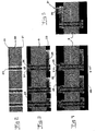
- the starting material is formed by a sheet 20 of an electrically insulating material.
- This sheet is, on its two flat sides, provided with a layer 21 of a conducting material. It may, for instance, be copper to a thickness of 5 ⁇ m.
- This plate is bored so as to obtain holes 22 in correspondence to the pattern board to be tested by means of the adapter board.
- Protective masks 23 are next provided on the sides of the pattern board. These protective masks leave openings at such places 24 where metal is to be plated. It appears from Fig 3 that plating, for instance by means of copper, has been carried out such that there has been applied, on the walls of the hole 22, a connecting plating 25 in substantially cylindrical shape and extending between the contact pads 26 on the lower side of the adapter board and part-contact pads 27 on the opposite side.
- a further application of a protective mask 28 is then made on the two sides of the adapter board 8, the lower protective mask 28 covering the entire lower side of the board, whereas the upper mask leaves openings 29. These openings are filled with conducting material in a plating following thereafter.
- plating may be carried out both electrolytically and in some other way.
- the material plated in the openings 29 forms part-contact pads 30 located on top of the previously mentioned part-contact pads 27.
- the part-contact pads 27 and 30 together form a contact pad generally denoted 31, the height of said contact pad suitably being in the order of twice as large as the height of the conducting paths 17, 18.
- the plating 25 in the hole 22 extends substantially equally much outwardly from both sides of the adapter board 8 as the thickness of the conducting paths 17, 18.
- the contact pad 31 is, in the example, twice as high as the conducting paths 17, 18.
- the adapter board 8 is then processed such that the protective masks 23, 28 are removed. This leads to the configuration of Figs 6 and 7.
- the contact pad 31 comprises an outwardly protruding part-contact pad 30 on a conducting path portion 17.
- the part-contact pad 30 has an external surface 32 which is substantially planar and extends substantially parallel to the plane of the adapter board 8.
- the part-contact pad 30 comprises rather sharp corners 33, involving a risk of damaging the rubber mat 13.
- the adapter board is conceived to have been subjected to an etching operation, which has caused the contact pad 31 to have been chamfered or rounded at its extreme end as is indicated at 34. Accordingly, the sharp edge (90°) appearing at 33 in Fig 6 has been smoothed so that on application against the rubber mat 13 a more lenient contact is obtained.
- etching used herein is to be understood as such a material-removing influence on the plated material on the adapter board 8 that a material removal occurs over the surface of the adapter board 8 so that after etching the different contact pads 31 will comprise substantially equal mutual relations as before the etching.
- the size of the contact pads 31 will be reduced by means of the etching. This means, accordingly, that the preceding plating must have been carried out to a larger size than the size finally intended after etching. More specifically, the area of the externally facing contact surfaces of the contact pads 31 as well as the thickness of the contact pads perpendicularly to the plane of the adapter board are reduced on etching.
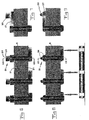
- a sheet 35 of an electrically conducting material is used as a starting material, such sheet having layers 36 of electrically conducting material, e.g. copper to a thickness of 5 ⁇ m, deposited on the sheet.
- a further conducting layer is plated on both sides of the sheet 35 as indicated in Fig 11. More specifically, copper may again be involved, for instance to a total thickness of 20+5 ⁇ m. In this plating, also the walls of the holes 38 is provided with a plated conducting material.
- an etching resist 39 is then applied on such places of the adapter board where the conducting, plated mateirial should remain. Thereafter, see Fig 13, the plated material not covered by the etching resist 39 is etched away so that only the portions present under the etching resist 39 remain as electrical conductors. The etching resist is then removed so that the situation according to Fig 14 is obtained.
- the contact element comprises here a contact pad 40 on one side of the adapter board and a contact pad 41 on the other side.
- the contact pad 40 is here conceived to have an annular configuration, i.e. be formed by a ring of electrically conducting material extending about the through hole 42.
- Fig 16 illustrates a variant similar to the one in Figs 15 and 16 in the sense that the plating on the wall of the hole through the adapter board 8 forms parts of a substantially annular contact pad 45. This consists of two part-contact pads 46, 47, which have been plated in two steps similar to what has been described in the embodiment according to Fig 2-9.
- the etching carried out has also here given rise to the peripherical edge of the contact pad being chamfered or rounded so as to obtain a minimum of wear/cutting on contact to the rubber mat 13.
Landscapes
- Engineering & Computer Science (AREA)
- Manufacturing & Machinery (AREA)
- Microelectronics & Electronic Packaging (AREA)
- Power Engineering (AREA)
- Physics & Mathematics (AREA)
- General Physics & Mathematics (AREA)
- Printing Elements For Providing Electric Connections Between Printed Circuits (AREA)
- Measuring Leads Or Probes (AREA)
Claims (5)
- Verfahren zur Herstellung von Kontaktplatten (10; 31; 40; 45) auf einer Adapterkarte (8), das eine Plattierungsbehandlung zum Aufbringen elektrisch leitenden Materials auf die Karte entsprechend den gewünschten Kontaktplatten umfasst, dadurch gekennzeichnet, dass das elektrisch leitende Material an den Kontaktplatten einem Ätzen unterzogen wird, um ein Abschrägen oder Abrunden von Umfangsrändern (33, 43) der Kontaktplatten vorzusehen.
- Verfahren nach Anspruch 1, dadurch gekennzeichnet, dass die Plattierungsbehandlung so ausgeführt wird, dass die Kontaktplatten eine größere Größe erhalten als jene, die letztlich beabsichtigt ist, und dass die Reduzierung der Größe auf die beabsichtigte Größe mithilfe des Ätzens ausgeführt wird.
- Verfahren nach Anspruch 2, dadurch gekennzeichnet, dass die Plattierungsbehandlung so ausgeführt wird, dass die Kontaktplatten auf ihren nach außen gerichteten. Kontaktoberflächen größere Bereiche erhalten als jener, der letztlich beabsichtigt ist, und dass die Reduzierung der Bereiche auf den letztlich beabsichtigten mithilfe des Ätzens ausgeführt wird.
- Verfahren nach Anspruch 2 oder 3, dadurch gekennzeichnet, dass die Plattierungsbehandlung so ausgeführt wird, dass die Dicke der Kontaktplatten größer ist als diejenige, die letztlich beabsichtigt ist, und dass die Reduzierung der Dicke auf die letztlich beabsichtigte Dicke mithilfe des Ätzens ausgeführt wird.
- Adapterkarte (8) zur Verwendung in einem Gerät zum Prüfen von Musterplatten, die mit elektrisch leitenden Bahnen versehen sind, wobei die Adapterkarte (8) auf einer ersten Seite (9) erste elektrisch leitende Stellen (31; 40; 45) in Form von Kontaktplatten, die in Kontakt mit elektrisch leitenden Stellen auf einer zu prüfenden Musterplatte gebracht werden sollen, und auf einer zweiten Seite (11) zweite elektrisch leitende Stellen umfasst, die Prüfkontaktpunkte des Testgeräts kontaktieren sollen, und dadurch gekennzeichnet, dass die Kontaktplatten (31; 40; 45) auf der ersten Seite der Adapterkarte mit abgeschrägten oder abgerundeten Umfangsrändern versehen sind.
Applications Claiming Priority (3)
| Application Number | Priority Date | Filing Date | Title |
|---|---|---|---|
| SE9503893A SE505383C2 (sv) | 1995-11-06 | 1995-11-06 | Förfarande för tillverkning av kontaktplattor på mönsterkort samt adapterkort för användning vid en apparat för testning av med elektriska ledningsbanor försedda mönsterkort |
| SE9503893 | 1995-11-06 | ||
| PCT/SE1996/001424 WO1997017822A1 (en) | 1995-11-06 | 1996-11-06 | Method for producing contact pads on pattern boards and adapter board for testing pattern boards |
Publications (2)
| Publication Number | Publication Date |
|---|---|
| EP0860101A1 EP0860101A1 (de) | 1998-08-26 |
| EP0860101B1 true EP0860101B1 (de) | 2004-10-20 |
Family
ID=20400078
Family Applications (1)
| Application Number | Title | Priority Date | Filing Date |
|---|---|---|---|
| EP96938583A Expired - Lifetime EP0860101B1 (de) | 1995-11-06 | 1996-11-06 | Verfahren zur herstellung von kontaktlöchern auf adapterplatten und adapterplatte zur prüfung von musterplatten |
Country Status (4)
| Country | Link |
|---|---|
| EP (1) | EP0860101B1 (de) |
| DE (1) | DE69633678D1 (de) |
| SE (1) | SE505383C2 (de) |
| WO (1) | WO1997017822A1 (de) |
Family Cites Families (5)
| Publication number | Priority date | Publication date | Assignee | Title |
|---|---|---|---|---|
| DE3638372A1 (de) * | 1986-11-11 | 1988-05-26 | Lang Dahlke Helmut | Vorrichtung zum pruefen von elektrischen leiterplatten |
| SE458005B (sv) * | 1987-11-16 | 1989-02-13 | Reinhold Strandberg | Foerfarande foer provning av kretskort samt apparat foer utfoerande av provningen |
| DE3925505A1 (de) * | 1989-04-05 | 1990-10-11 | Siemens Ag | Vorrichtung zum pruefen von leiterplatten |
| DE4226069C2 (de) * | 1992-08-06 | 1994-08-04 | Test Plus Electronic Gmbh | Adaptereinrichtung für eine Prüfeinrichtung für Schaltungsplatinen |
| JP2710544B2 (ja) * | 1993-09-30 | 1998-02-10 | インターナショナル・ビジネス・マシーンズ・コーポレイション | プローブ構造、プローブ構造の形成方法 |
-
1995
- 1995-11-06 SE SE9503893A patent/SE505383C2/sv not_active IP Right Cessation
-
1996
- 1996-11-06 DE DE69633678T patent/DE69633678D1/de not_active Expired - Fee Related
- 1996-11-06 EP EP96938583A patent/EP0860101B1/de not_active Expired - Lifetime
- 1996-11-06 WO PCT/SE1996/001424 patent/WO1997017822A1/en not_active Ceased
Also Published As
| Publication number | Publication date |
|---|---|
| WO1997017822A1 (en) | 1997-05-15 |
| EP0860101A1 (de) | 1998-08-26 |
| SE505383C2 (sv) | 1997-08-18 |
| SE9503893L (sv) | 1997-05-07 |
| SE9503893D0 (sv) | 1995-11-06 |
| DE69633678D1 (de) | 2004-11-25 |
Similar Documents
| Publication | Publication Date | Title |
|---|---|---|
| US5133119A (en) | Shearing stress interconnection apparatus and method | |
| US4340860A (en) | Integrated circuit carrier package test probe | |
| DE69635603T2 (de) | Höckerkontakt für eine Leiterplatte und Halbleitermodul mit derselben | |
| US6351885B2 (en) | Method of making conductive bump on wiring board | |
| US5451169A (en) | Connector with monolithic multi-contact array | |
| EP1019986B1 (de) | Leiterplattenkonstruktionen und deren herstellungsverfahren | |
| US6160412A (en) | Impedance-matched interconnection device for connecting a vertical-pin integrated circuit probing device to integrated circuit test equipment | |
| US4965702A (en) | Chip carrier package and method of manufacture | |
| EP0667962B1 (de) | Testanordnung mit filmadaptor fuer leiterplatten | |
| US5126818A (en) | Semiconductor device | |
| US5963045A (en) | Method for testing circuit board assemblies | |
| JP3467394B2 (ja) | バーンイン用ウェハカセット及びプローブカードの製造方法 | |
| US5203078A (en) | Printed wiring board for IC cards | |
| US5899757A (en) | Compression connector | |
| US4891014A (en) | Method of forming contact bumps in contact pads | |
| JPH0935789A (ja) | 異方導電性シートおよびその製造方法 | |
| US6948242B2 (en) | Process for producing a contact-making device | |
| US5261158A (en) | Method of forming a resilient interconnection bridge | |
| US6641406B1 (en) | Flexible connector for high density circuit applications | |
| EP0860101B1 (de) | Verfahren zur herstellung von kontaktlöchern auf adapterplatten und adapterplatte zur prüfung von musterplatten | |
| US5296082A (en) | Mold for printed wiring board | |
| EP0231384B1 (de) | Ein Verfahren zum Herstellen einer gedruckten Schaltungsplatte für Halbleiterschaltungen | |
| KR101846303B1 (ko) | 양방향 도전성 모듈, 반도체 테스트 소켓, 그리고 그 제조방법 | |
| US6196042B1 (en) | Coining tool and process of manufacturing same for making connection components | |
| JPH0772172A (ja) | 回路基板検査機 |
Legal Events
| Date | Code | Title | Description |
|---|---|---|---|
| PUAI | Public reference made under article 153(3) epc to a published international application that has entered the european phase |
Free format text: ORIGINAL CODE: 0009012 |
|
| 17P | Request for examination filed |
Effective date: 19980429 |
|
| AK | Designated contracting states |
Kind code of ref document: A1 Designated state(s): CH DE DK FI FR GB IT LI NL SE |
|
| 17Q | First examination report despatched |
Effective date: 20021024 |
|
| RTI1 | Title (correction) |
Free format text: METHOD FOR PRODUCING CONTACT PADS ON ADAPTER BOARDS AND ADAPTER BOARD FOR TESTING PATTERN BOARDS |
|
| GRAP | Despatch of communication of intention to grant a patent |
Free format text: ORIGINAL CODE: EPIDOSNIGR1 |
|
| RTI1 | Title (correction) |
Free format text: METHOD FOR PRODUCING CONTACT PADS ON ADAPTER BOARDS AND ADAPTER BOARD FOR TESTING PATTERN BOARDS |
|
| GRAS | Grant fee paid |
Free format text: ORIGINAL CODE: EPIDOSNIGR3 |
|
| GRAA | (expected) grant |
Free format text: ORIGINAL CODE: 0009210 |
|
| AK | Designated contracting states |
Kind code of ref document: B1 Designated state(s): CH DE DK FI FR GB IT LI NL SE |
|
| PG25 | Lapsed in a contracting state [announced via postgrant information from national office to epo] |
Ref country code: NL Free format text: LAPSE BECAUSE OF FAILURE TO SUBMIT A TRANSLATION OF THE DESCRIPTION OR TO PAY THE FEE WITHIN THE PRESCRIBED TIME-LIMIT Effective date: 20041020 Ref country code: LI Free format text: LAPSE BECAUSE OF FAILURE TO SUBMIT A TRANSLATION OF THE DESCRIPTION OR TO PAY THE FEE WITHIN THE PRESCRIBED TIME-LIMIT Effective date: 20041020 Ref country code: IT Free format text: LAPSE BECAUSE OF FAILURE TO SUBMIT A TRANSLATION OF THE DESCRIPTION OR TO PAY THE FEE WITHIN THE PRE;WARNING: LAPSES OF ITALIAN PATENTS WITH EFFECTIVE DATE BEFORE 2007 MAY HAVE OCCURRED AT ANY TIME BEFORE 2007. THE CORRECT EFFECTIVE DATE MAY BE DIFFERENT FROM THE ONE RECORDED.SCRIBED TIME-LIMIT Effective date: 20041020 Ref country code: FR Free format text: LAPSE BECAUSE OF FAILURE TO SUBMIT A TRANSLATION OF THE DESCRIPTION OR TO PAY THE FEE WITHIN THE PRESCRIBED TIME-LIMIT Effective date: 20041020 Ref country code: FI Free format text: LAPSE BECAUSE OF FAILURE TO SUBMIT A TRANSLATION OF THE DESCRIPTION OR TO PAY THE FEE WITHIN THE PRESCRIBED TIME-LIMIT Effective date: 20041020 Ref country code: CH Free format text: LAPSE BECAUSE OF FAILURE TO SUBMIT A TRANSLATION OF THE DESCRIPTION OR TO PAY THE FEE WITHIN THE PRESCRIBED TIME-LIMIT Effective date: 20041020 |
|
| REG | Reference to a national code |
Ref country code: GB Ref legal event code: FG4D |
|
| REG | Reference to a national code |
Ref country code: CH Ref legal event code: EP |
|
| REF | Corresponds to: |
Ref document number: 69633678 Country of ref document: DE Date of ref document: 20041125 Kind code of ref document: P |
|
| PGFP | Annual fee paid to national office [announced via postgrant information from national office to epo] |
Ref country code: SE Payment date: 20041215 Year of fee payment: 9 |
|
| PG25 | Lapsed in a contracting state [announced via postgrant information from national office to epo] |
Ref country code: GB Free format text: LAPSE BECAUSE OF NON-PAYMENT OF DUE FEES Effective date: 20050120 Ref country code: DK Free format text: LAPSE BECAUSE OF FAILURE TO SUBMIT A TRANSLATION OF THE DESCRIPTION OR TO PAY THE FEE WITHIN THE PRESCRIBED TIME-LIMIT Effective date: 20050120 |
|
| REG | Reference to a national code |
Ref country code: SE Ref legal event code: TRGR |
|
| REG | Reference to a national code |
Ref country code: CH Ref legal event code: PL |
|
| NLV1 | Nl: lapsed or annulled due to failure to fulfill the requirements of art. 29p and 29m of the patents act | ||
| PG25 | Lapsed in a contracting state [announced via postgrant information from national office to epo] |
Ref country code: DE Free format text: LAPSE BECAUSE OF NON-PAYMENT OF DUE FEES Effective date: 20050601 |
|
| PLBE | No opposition filed within time limit |
Free format text: ORIGINAL CODE: 0009261 |
|
| STAA | Information on the status of an ep patent application or granted ep patent |
Free format text: STATUS: NO OPPOSITION FILED WITHIN TIME LIMIT |
|
| GBPC | Gb: european patent ceased through non-payment of renewal fee |
Effective date: 20050120 |
|
| 26N | No opposition filed |
Effective date: 20050721 |
|
| PG25 | Lapsed in a contracting state [announced via postgrant information from national office to epo] |
Ref country code: SE Free format text: LAPSE BECAUSE OF NON-PAYMENT OF DUE FEES Effective date: 20051107 |
|
| EN | Fr: translation not filed | ||
| EUG | Se: european patent has lapsed |