EP0854523B1 - Semiconductor light emitting device and its manufacturing method - Google Patents
Semiconductor light emitting device and its manufacturing method Download PDFInfo
- Publication number
- EP0854523B1 EP0854523B1 EP98100627A EP98100627A EP0854523B1 EP 0854523 B1 EP0854523 B1 EP 0854523B1 EP 98100627 A EP98100627 A EP 98100627A EP 98100627 A EP98100627 A EP 98100627A EP 0854523 B1 EP0854523 B1 EP 0854523B1
- Authority
- EP
- European Patent Office
- Prior art keywords
- light emitting
- semiconductor light
- resin
- emitting device
- encapsulating
- Prior art date
- Legal status (The legal status is an assumption and is not a legal conclusion. Google has not performed a legal analysis and makes no representation as to the accuracy of the status listed.)
- Expired - Lifetime
Links
Images


Classifications
-
- H—ELECTRICITY
- H01—ELECTRIC ELEMENTS
- H01L—SEMICONDUCTOR DEVICES NOT COVERED BY CLASS H10
- H01L33/00—Semiconductor devices with at least one potential-jump barrier or surface barrier specially adapted for light emission; Processes or apparatus specially adapted for the manufacture or treatment thereof or of parts thereof; Details thereof
- H01L33/48—Semiconductor devices with at least one potential-jump barrier or surface barrier specially adapted for light emission; Processes or apparatus specially adapted for the manufacture or treatment thereof or of parts thereof; Details thereof characterised by the semiconductor body packages
- H01L33/483—Containers
- H01L33/486—Containers adapted for surface mounting
-
- H—ELECTRICITY
- H01—ELECTRIC ELEMENTS
- H01L—SEMICONDUCTOR DEVICES NOT COVERED BY CLASS H10
- H01L33/00—Semiconductor devices with at least one potential-jump barrier or surface barrier specially adapted for light emission; Processes or apparatus specially adapted for the manufacture or treatment thereof or of parts thereof; Details thereof
-
- H—ELECTRICITY
- H01—ELECTRIC ELEMENTS
- H01L—SEMICONDUCTOR DEVICES NOT COVERED BY CLASS H10
- H01L2224/00—Indexing scheme for arrangements for connecting or disconnecting semiconductor or solid-state bodies and methods related thereto as covered by H01L24/00
- H01L2224/01—Means for bonding being attached to, or being formed on, the surface to be connected, e.g. chip-to-package, die-attach, "first-level" interconnects; Manufacturing methods related thereto
- H01L2224/26—Layer connectors, e.g. plate connectors, solder or adhesive layers; Manufacturing methods related thereto
- H01L2224/31—Structure, shape, material or disposition of the layer connectors after the connecting process
- H01L2224/32—Structure, shape, material or disposition of the layer connectors after the connecting process of an individual layer connector
- H01L2224/321—Disposition
- H01L2224/32151—Disposition the layer connector connecting between a semiconductor or solid-state body and an item not being a semiconductor or solid-state body, e.g. chip-to-substrate, chip-to-passive
- H01L2224/32221—Disposition the layer connector connecting between a semiconductor or solid-state body and an item not being a semiconductor or solid-state body, e.g. chip-to-substrate, chip-to-passive the body and the item being stacked
- H01L2224/32245—Disposition the layer connector connecting between a semiconductor or solid-state body and an item not being a semiconductor or solid-state body, e.g. chip-to-substrate, chip-to-passive the body and the item being stacked the item being metallic
-
- H—ELECTRICITY
- H01—ELECTRIC ELEMENTS
- H01L—SEMICONDUCTOR DEVICES NOT COVERED BY CLASS H10
- H01L2224/00—Indexing scheme for arrangements for connecting or disconnecting semiconductor or solid-state bodies and methods related thereto as covered by H01L24/00
- H01L2224/01—Means for bonding being attached to, or being formed on, the surface to be connected, e.g. chip-to-package, die-attach, "first-level" interconnects; Manufacturing methods related thereto
- H01L2224/42—Wire connectors; Manufacturing methods related thereto
- H01L2224/44—Structure, shape, material or disposition of the wire connectors prior to the connecting process
- H01L2224/45—Structure, shape, material or disposition of the wire connectors prior to the connecting process of an individual wire connector
- H01L2224/45001—Core members of the connector
- H01L2224/45099—Material
- H01L2224/451—Material with a principal constituent of the material being a metal or a metalloid, e.g. boron (B), silicon (Si), germanium (Ge), arsenic (As), antimony (Sb), tellurium (Te) and polonium (Po), and alloys thereof
- H01L2224/45138—Material with a principal constituent of the material being a metal or a metalloid, e.g. boron (B), silicon (Si), germanium (Ge), arsenic (As), antimony (Sb), tellurium (Te) and polonium (Po), and alloys thereof the principal constituent melting at a temperature of greater than or equal to 950°C and less than 1550°C
- H01L2224/45144—Gold (Au) as principal constituent
-
- H—ELECTRICITY
- H01—ELECTRIC ELEMENTS
- H01L—SEMICONDUCTOR DEVICES NOT COVERED BY CLASS H10
- H01L2224/00—Indexing scheme for arrangements for connecting or disconnecting semiconductor or solid-state bodies and methods related thereto as covered by H01L24/00
- H01L2224/01—Means for bonding being attached to, or being formed on, the surface to be connected, e.g. chip-to-package, die-attach, "first-level" interconnects; Manufacturing methods related thereto
- H01L2224/42—Wire connectors; Manufacturing methods related thereto
- H01L2224/47—Structure, shape, material or disposition of the wire connectors after the connecting process
- H01L2224/48—Structure, shape, material or disposition of the wire connectors after the connecting process of an individual wire connector
- H01L2224/4805—Shape
- H01L2224/4809—Loop shape
- H01L2224/48091—Arched
-
- H—ELECTRICITY
- H01—ELECTRIC ELEMENTS
- H01L—SEMICONDUCTOR DEVICES NOT COVERED BY CLASS H10
- H01L2224/00—Indexing scheme for arrangements for connecting or disconnecting semiconductor or solid-state bodies and methods related thereto as covered by H01L24/00
- H01L2224/01—Means for bonding being attached to, or being formed on, the surface to be connected, e.g. chip-to-package, die-attach, "first-level" interconnects; Manufacturing methods related thereto
- H01L2224/42—Wire connectors; Manufacturing methods related thereto
- H01L2224/47—Structure, shape, material or disposition of the wire connectors after the connecting process
- H01L2224/48—Structure, shape, material or disposition of the wire connectors after the connecting process of an individual wire connector
- H01L2224/481—Disposition
- H01L2224/48151—Connecting between a semiconductor or solid-state body and an item not being a semiconductor or solid-state body, e.g. chip-to-substrate, chip-to-passive
- H01L2224/48221—Connecting between a semiconductor or solid-state body and an item not being a semiconductor or solid-state body, e.g. chip-to-substrate, chip-to-passive the body and the item being stacked
- H01L2224/48245—Connecting between a semiconductor or solid-state body and an item not being a semiconductor or solid-state body, e.g. chip-to-substrate, chip-to-passive the body and the item being stacked the item being metallic
- H01L2224/48247—Connecting between a semiconductor or solid-state body and an item not being a semiconductor or solid-state body, e.g. chip-to-substrate, chip-to-passive the body and the item being stacked the item being metallic connecting the wire to a bond pad of the item
-
- H—ELECTRICITY
- H01—ELECTRIC ELEMENTS
- H01L—SEMICONDUCTOR DEVICES NOT COVERED BY CLASS H10
- H01L2224/00—Indexing scheme for arrangements for connecting or disconnecting semiconductor or solid-state bodies and methods related thereto as covered by H01L24/00
- H01L2224/01—Means for bonding being attached to, or being formed on, the surface to be connected, e.g. chip-to-package, die-attach, "first-level" interconnects; Manufacturing methods related thereto
- H01L2224/42—Wire connectors; Manufacturing methods related thereto
- H01L2224/47—Structure, shape, material or disposition of the wire connectors after the connecting process
- H01L2224/48—Structure, shape, material or disposition of the wire connectors after the connecting process of an individual wire connector
- H01L2224/484—Connecting portions
- H01L2224/48463—Connecting portions the connecting portion on the bonding area of the semiconductor or solid-state body being a ball bond
- H01L2224/48465—Connecting portions the connecting portion on the bonding area of the semiconductor or solid-state body being a ball bond the other connecting portion not on the bonding area being a wedge bond, i.e. ball-to-wedge, regular stitch
-
- H—ELECTRICITY
- H01—ELECTRIC ELEMENTS
- H01L—SEMICONDUCTOR DEVICES NOT COVERED BY CLASS H10
- H01L2224/00—Indexing scheme for arrangements for connecting or disconnecting semiconductor or solid-state bodies and methods related thereto as covered by H01L24/00
- H01L2224/73—Means for bonding being of different types provided for in two or more of groups H01L2224/10, H01L2224/18, H01L2224/26, H01L2224/34, H01L2224/42, H01L2224/50, H01L2224/63, H01L2224/71
- H01L2224/732—Location after the connecting process
- H01L2224/73251—Location after the connecting process on different surfaces
- H01L2224/73265—Layer and wire connectors
-
- H—ELECTRICITY
- H01—ELECTRIC ELEMENTS
- H01L—SEMICONDUCTOR DEVICES NOT COVERED BY CLASS H10
- H01L2224/00—Indexing scheme for arrangements for connecting or disconnecting semiconductor or solid-state bodies and methods related thereto as covered by H01L24/00
- H01L2224/91—Methods for connecting semiconductor or solid state bodies including different methods provided for in two or more of groups H01L2224/80 - H01L2224/90
- H01L2224/92—Specific sequence of method steps
- H01L2224/922—Connecting different surfaces of the semiconductor or solid-state body with connectors of different types
- H01L2224/9222—Sequential connecting processes
- H01L2224/92242—Sequential connecting processes the first connecting process involving a layer connector
- H01L2224/92247—Sequential connecting processes the first connecting process involving a layer connector the second connecting process involving a wire connector
-
- H—ELECTRICITY
- H01—ELECTRIC ELEMENTS
- H01L—SEMICONDUCTOR DEVICES NOT COVERED BY CLASS H10
- H01L2924/00—Indexing scheme for arrangements or methods for connecting or disconnecting semiconductor or solid-state bodies as covered by H01L24/00
- H01L2924/01—Chemical elements
- H01L2924/01012—Magnesium [Mg]
-
- H—ELECTRICITY
- H01—ELECTRIC ELEMENTS
- H01L—SEMICONDUCTOR DEVICES NOT COVERED BY CLASS H10
- H01L2924/00—Indexing scheme for arrangements or methods for connecting or disconnecting semiconductor or solid-state bodies as covered by H01L24/00
- H01L2924/01—Chemical elements
- H01L2924/0102—Calcium [Ca]
-
- H—ELECTRICITY
- H01—ELECTRIC ELEMENTS
- H01L—SEMICONDUCTOR DEVICES NOT COVERED BY CLASS H10
- H01L2924/00—Indexing scheme for arrangements or methods for connecting or disconnecting semiconductor or solid-state bodies as covered by H01L24/00
- H01L2924/01—Chemical elements
- H01L2924/01025—Manganese [Mn]
-
- H—ELECTRICITY
- H01—ELECTRIC ELEMENTS
- H01L—SEMICONDUCTOR DEVICES NOT COVERED BY CLASS H10
- H01L2924/00—Indexing scheme for arrangements or methods for connecting or disconnecting semiconductor or solid-state bodies as covered by H01L24/00
- H01L2924/01—Chemical elements
- H01L2924/01039—Yttrium [Y]
-
- H—ELECTRICITY
- H01—ELECTRIC ELEMENTS
- H01L—SEMICONDUCTOR DEVICES NOT COVERED BY CLASS H10
- H01L2924/00—Indexing scheme for arrangements or methods for connecting or disconnecting semiconductor or solid-state bodies as covered by H01L24/00
- H01L2924/01—Chemical elements
- H01L2924/01063—Europium [Eu]
-
- H—ELECTRICITY
- H01—ELECTRIC ELEMENTS
- H01L—SEMICONDUCTOR DEVICES NOT COVERED BY CLASS H10
- H01L2924/00—Indexing scheme for arrangements or methods for connecting or disconnecting semiconductor or solid-state bodies as covered by H01L24/00
- H01L2924/01—Chemical elements
- H01L2924/01079—Gold [Au]
-
- H—ELECTRICITY
- H01—ELECTRIC ELEMENTS
- H01L—SEMICONDUCTOR DEVICES NOT COVERED BY CLASS H10
- H01L2933/00—Details relating to devices covered by the group H01L33/00 but not provided for in its subgroups
- H01L2933/0091—Scattering means in or on the semiconductor body or semiconductor body package
-
- H—ELECTRICITY
- H01—ELECTRIC ELEMENTS
- H01L—SEMICONDUCTOR DEVICES NOT COVERED BY CLASS H10
- H01L33/00—Semiconductor devices with at least one potential-jump barrier or surface barrier specially adapted for light emission; Processes or apparatus specially adapted for the manufacture or treatment thereof or of parts thereof; Details thereof
- H01L33/48—Semiconductor devices with at least one potential-jump barrier or surface barrier specially adapted for light emission; Processes or apparatus specially adapted for the manufacture or treatment thereof or of parts thereof; Details thereof characterised by the semiconductor body packages
- H01L33/50—Wavelength conversion elements
- H01L33/505—Wavelength conversion elements characterised by the shape, e.g. plate or foil
-
- H—ELECTRICITY
- H01—ELECTRIC ELEMENTS
- H01L—SEMICONDUCTOR DEVICES NOT COVERED BY CLASS H10
- H01L33/00—Semiconductor devices with at least one potential-jump barrier or surface barrier specially adapted for light emission; Processes or apparatus specially adapted for the manufacture or treatment thereof or of parts thereof; Details thereof
- H01L33/48—Semiconductor devices with at least one potential-jump barrier or surface barrier specially adapted for light emission; Processes or apparatus specially adapted for the manufacture or treatment thereof or of parts thereof; Details thereof characterised by the semiconductor body packages
- H01L33/50—Wavelength conversion elements
- H01L33/507—Wavelength conversion elements the elements being in intimate contact with parts other than the semiconductor body or integrated with parts other than the semiconductor body
-
- H—ELECTRICITY
- H01—ELECTRIC ELEMENTS
- H01L—SEMICONDUCTOR DEVICES NOT COVERED BY CLASS H10
- H01L33/00—Semiconductor devices with at least one potential-jump barrier or surface barrier specially adapted for light emission; Processes or apparatus specially adapted for the manufacture or treatment thereof or of parts thereof; Details thereof
- H01L33/48—Semiconductor devices with at least one potential-jump barrier or surface barrier specially adapted for light emission; Processes or apparatus specially adapted for the manufacture or treatment thereof or of parts thereof; Details thereof characterised by the semiconductor body packages
- H01L33/52—Encapsulations
- H01L33/54—Encapsulations having a particular shape
-
- H—ELECTRICITY
- H01—ELECTRIC ELEMENTS
- H01L—SEMICONDUCTOR DEVICES NOT COVERED BY CLASS H10
- H01L33/00—Semiconductor devices with at least one potential-jump barrier or surface barrier specially adapted for light emission; Processes or apparatus specially adapted for the manufacture or treatment thereof or of parts thereof; Details thereof
- H01L33/48—Semiconductor devices with at least one potential-jump barrier or surface barrier specially adapted for light emission; Processes or apparatus specially adapted for the manufacture or treatment thereof or of parts thereof; Details thereof characterised by the semiconductor body packages
- H01L33/58—Optical field-shaping elements
- H01L33/60—Reflective elements
-
- H—ELECTRICITY
- H01—ELECTRIC ELEMENTS
- H01L—SEMICONDUCTOR DEVICES NOT COVERED BY CLASS H10
- H01L33/00—Semiconductor devices with at least one potential-jump barrier or surface barrier specially adapted for light emission; Processes or apparatus specially adapted for the manufacture or treatment thereof or of parts thereof; Details thereof
- H01L33/48—Semiconductor devices with at least one potential-jump barrier or surface barrier specially adapted for light emission; Processes or apparatus specially adapted for the manufacture or treatment thereof or of parts thereof; Details thereof characterised by the semiconductor body packages
- H01L33/62—Arrangements for conducting electric current to or from the semiconductor body, e.g. lead-frames, wire-bonds or solder balls
Landscapes
- Engineering & Computer Science (AREA)
- Microelectronics & Electronic Packaging (AREA)
- Manufacturing & Machinery (AREA)
- Computer Hardware Design (AREA)
- Power Engineering (AREA)
- Led Device Packages (AREA)
Description
- This invention relates to a semiconductor light emitting device used in indicators, message boards, or other visual display devices, which is improved in adherability of a resin encapsulating element and a resin stem, and also relates to a method for manufacturing same.
- In conventional semiconductor light emitting devices, after a semiconductor light emitting element is mounted and bonded to a printed board with a printed wiring, a light-transmissive resin is injected into a cavity defined by a case mold capped onto the printed board to form an encapsulating element having a lens function.
- These semiconductor light emitting devices are expensive, and the injected resin often leaks. Moreover, chips, unfilled portions or bubbles are liable to be made in the encapsulating element, resulting that the devices are not satisfactory in their appearances. Additionally, the use of an expensive printed board and a slow injection speed cause a high manufacturing cost.
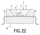
- On the other hand, a surface-packaged semiconductor light emitting device having no lens is as shown in Fig. 22. A
resin stem 10 has formed arecess 7, and a semiconductorlight emitting element 1 is put on the bottom of therecess 7. Thesloped side walls 8 of therecess 7 functions as light reflective surfaces.Leads resin stem 10. Theleads resin stem 10 is made by injection-molding a thermoplastic resin such as polycarbonate (PC) containing a filler agent such as silica (SiO2) together with the lead frame. End portions of theleads recess 7 of theresin stem 10. The semiconductorlight emitting element 1 is mounted on thelead 21 byconductive paste 3, or the like, containing silver (Ag), for example. A first electrode of the semiconductorlight emitting element 1 is connected to thelead 21, and a second electrode is electrically connected to thelead 22. The second electrode and thelead 22 are connected by a bondingwire 4 of gold (Au), for example. A light-transmissive resin encapsulatingelement 5 of a thermosetting resin is applied onto theresin stem 10 so as to cover these end portions of theleads light emitting element 1 and bondingwire 4. - However, the surface-packaged semiconductor light emitting device shown in Fig. 22 has no lens, and is unreliable in adherability between the resin encapsulating element of a thermosetting resin and a resin stem of a thermoplastic resin.
-
US-5,266,817 describes a package structure of a multi-chip light emitting diode. The LED includes a base having a recess formed thereon and a transparent housing disposed over the base. A conductive plate is mounted in the recess with chips of different colour thereon, which are all enclosed by the housing. The base is made by molding injection and of transparent or translucent material. A plurality of pins are provided, which on the one hand contact respective chips or the conductive plate, and on the other hand extend downward and out of the base. -
US-5,040,868 describes a surface-mountable opto-component. The opto-component has at least one base member which contains at least one depression, in which an opto-transmitter or opto-receiver can be arranged. The depressions can be cast out with plastic. -
DE 43 408 64 A1 describes a device and method for manufacturing opto-electronic elements. The document describes dipping matrix stripes into a resin. - It is therefore an object of the invention to provide an inexpensive semiconductor light emitting device and its manufacturing method, which permits a lens to be made easily, and is improved in adherability and humidity resistance between the resin encapsulating element and the resin stem, and also improved in reflecting efficiency and light take-out efficiency.
- This objet is solvent by the subject matter of the independent claims. Advantageous embodiments are described in the dependent claims.
- According to the invention, there is provided a semiconductor light emitting device according to
claim 1, wherein the semiconductor light emitting chip is made by using GaP, GaAlAs, GaAsP, InGaAlP, GaN, ZnSe, SiC, BN, for example. - The resin stem may have at least one through hole in the bottom of the recess or at least one through hole extending from the upper surface to the lower surface. The projection may form a lens having a vertical axis aligned with a vertical axis of the resin stem, and these center axes may be aligned with a vertical axis of the semiconductor light emitting element. The semiconductor light emitting device may include a fluorescent element for converting light emanating from the semiconductor light emitting element into different wavelength light. The fluorescent element may be contained in the resin portion of the resin stem, may be applied onto inner wall surfaces of the recess of the resin stem, or may be contained in a mounting adhesive applied onto the bottom surface of the semiconductor light emitting element, in the light-transmissive resin filling the recess, or in the light-transmissive resin forming said projection.
- The recess of the resin stem may be longer in a first horizontal direction in which the first and second leads extends than in a second horizontal direction normal to the first direction. The first electrode of the semiconductor light emitting element may be connected to the first lead by a bonding wire, and the second electrode of the semiconductor light emitting element may be connected to the second lead by another bonding wire. The center of a horizontal cross-sectional configuration of the recess of the resin stem may be offset from the center of a horizontal cross-sectional configuration of the resin stem. The second electrode of the semiconductor light emitting element may be connected to the second lead by a bonding wire, and the center of a horizontal cross-sectional configuration of the recess of the resin stem may be offset from the center of a horizontal cross-sectional configuration of the resin stem toward the externally extending direction of the second lead. Inner side surfaces of the recess may serve as reflective surfaces.
- The resin portion of the resin stem is made from a thermoplastic resin not less than 65 weight % and a filler agent not more than 35 weight %, the filler agent being a high reflective material containing titanium oxide, silicon oxide, and/or aluminum oxide, and titanium oxide occupying 10 to 15 weight %.
- There is also provided a method for manufacturing a semiconductor light emitting device according to claim 17.
- In the semiconductor light emitting device according to the invention, since the projection of a light-transmissive resin is formed on the resin stem to envelope its upper surface and upper part of the side surfaces continuous from the upper surface, the adherability between the projection and the resin stem is improved. Ultraviolet irradiation improves the coupling force of the resin stem of a thermoplastic resin with a thermosetting light-transmissive resin. By aligning the semiconductor light emitting element with vertical center lines of the projection and the resin stem and by deviating the center of recess from the center of the resin stem, the light emitting efficiency is improved. The through hole formed in the resin stem facilitates coupling of the light-transmissive resin to the resin stem. The stopper keeps the projection distant from the lead frame (leads).
- The above-summarized constructions of the present invention remarkably increase the adherability between the projection of a light-transmissive thermosetting resin and the resin stem of a thermoplastic resin, and contributes to realization of an economical resin stem with a high reflective index. Moreover, the invention can cope with various applications by varying the lead forming configuration. Additionally, various semiconductor light emitting devices with different optical characteristics can be prepared by changing the encapsulating case mold.
-
- Fig. 1 is a cross-sectional view of a semiconductor light emitting device according to an embodiment of the invention (taken along the A-A' line of Fig. 2);
- Fig. 2 is a plan view of the semiconductor light emitting device according to the invention;
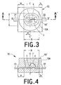
- Fig. 3 is a simplified plan view of a resin stem used in the invention;
- Fig. 4 is a cross-sectional view taken along the A-A' line of Fig. 3;
- Fig. 5 is a flow chart of a manufacturing process of the semiconductor light emitting device according to the invention;
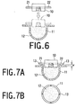
- Fig. 6 is a cross-sectional view of an encapsulating case mold and a resin stem used in the invention;
- Figs. 7A and 7B are a cross-sectional view and a plan view of the encapsulating case mold used in the invention respectively;
- Figs. 8A and 8B are an elevation view and a plan view of the resin portion of the resin stem used in the invention respectively;
- Figs. 9A and 9B are a plan view and a cross-sectional view of a semiconductor light emitting device according to the invention respectively;
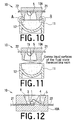
- Fig. 10 is a cross-sectional view of an encapsulating case mold and a resin stem used in the invention;
- Fig. 11 is a cross-sectional view of the encapsulating case mold and the resin stem used in the invention;
- Fig. 12 is a cross-sectional view of the resin stem used in the invention;
- Fig. 13 is a diagram showing changes in reflective index with composition ratio of titanium oxide;
- Fig. 14 is a diagram showing changes in adherability with ultraviolet radiation;
- Fig. 15 is a cross-sectional view of a semiconductor light emitting device according to the invention (taken along the A-A' line of Fig. 16);
- Fig. 16 is a plan view of the semiconductor light emitting device;
- Fig. 17 is a flow chart of a manufacturing process of the semiconductor light emitting device according to the invention;
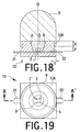
- Fig. 18 is a cross-sectional view of a semiconductor light emitting device according to the invention (taken along the A-A' line of Fig. 19);
- Fig. 19 is a plan view of the semiconductor light emitting device;
- Fig. 20 is a plan view of a lead frame used in the invention;
- Fig. 21 is a cross-sectional view of a series of case molds and a series of resin stems used in the invention;
- Fig. 22 is a cross-sectional view of a conventional semiconductor light emitting device;
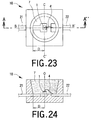
- Fig. 23 is a plan view of a conventional resin stem; and
- Fig. 24 is a cross-sectional view taken along the A-A' line of Fig. 23.
- Explained below are embodiments of the present invention with reference to the drawings. Referring to Figs. 1 through 4 showing a first embodiment, Fig. 1 is a cross-sectional view of a semiconductor light emitting device, and Fig. 2 is a plan view of the same semiconductor light emitting device. Fig. 1 is taken along the A-A' line of Fig. 2. Fig. 3 is a simplified plan view of a resin stem for explaining the position of the resin stem in the semiconductor light emitting device, and Fig. 4 is a cross-sectional view taken along the A-A' line of Fig. 3.
- As shown in Fig. 1, the
resin stem 10 has leads 21 and 22, made by molding a lead frame, and aresin portion 10A, which is an integral molded product. Theresin portion 10A includes a recess which opens to the upper surface thereof with a larger area than its bottom and has slanted side walls behaving asreflective surfaces 8. Theresin portion 10A of theresin stem 10 comprises a generally square lower portion and a generally circular upper portion having the recess. End portions ofleads leads resin portion 10A. These leads 21, 22 are molded in a cut-and-forming step of the lead frame. A semiconductorlight emitting element 1 made of GaP, GaAlAs, GaAsP, InGaAlP or GaN, for example, has first and second electrodes (not shown), and is mounted at thelead 21 on the bottom surface of the recess byAg paste 3, for example. - The second electrode of the semiconductor
light emitting element 1 is connected to thelead 22 by abonding wire 4 of Au, for example. A thermosetting resin fully fills the recess of theresin portion 10A to form a light-transmissiveresin encapsulating element 5. Aprojection 9 of a light-transmissive resin encapsulating element made of a thermosetting resin is formed on theresin stem 10. Theprojection 9 is used as a lens, for example. Theprojection 9 covers the entire upper surface of theresin stem 10 including the surface of theresin encapsulating element 5 and an upper part of the side surfaces continuous from the upper surface. The semiconductorlight emitting element 1 in the recess is located along a vertical center line O of theprojection 9. The center line O is common to the vertical center line of theresin stem 10. However, the recess is eccentric from the center of the upper surface of theresin stem 10, and the vertical center line O' of the recess does not coincide with the center line O. This construction results in locating the semiconductorlight emitting element 1 closer to thereflective surfaces 8 and in making thereflective surfaces 8 more effective to improve the light take-out efficiency. Theprojection 9 is larger than the diameter of the upper portion of theresin stem 10 by the thickness t so as to cover the entirety of the upper side surface of the resin stem 10 (length x). Theprojection 9 does not contact thelead leads - In this embodiment, the thickness t of the
projection 9 on the side surface of the resin stem is approximately 2 mm when the length of one side of theresin portion 10A is either 2.4 mm or 4.5 mm. When manufacturing the semiconductor light emitting device, after mounting theprojection 9 on theresin stem 10, a lead frame is cut and formed into the form ofleads - The structure of the resin stem of the semiconductor light emitting device shown in Fig. 1 is explained in greater detail with reference to Figs. 3 and 4 which are a simplified plan view and a cross-sectional view of the resin stem supporting the semiconductor light emitting element, removing the projection for clearly illustrating the position of the semiconductor light emitting element. The
resin portion 10A of theresin stem 10 is generally square or rectangular (approximately as large as 3.0×3.4 mm or 5.0×5.4 mm, for example), and the upper portion including the upper surface 10' is cylindrical. The B-B' line and the C-C' line in Fig. 3 are center lines of two pairs of parallel sides. The vertical center line O of theresin stem 10 is shown in Fig. 4. As stated above, the upper surface 10' of theresin stem 10 is generally circular, and therecess 7 formed therein is substantially elliptic (with the longest diameter R and the shortest diameter r). The leads 21 and 22 extend in opposite directions from their confronting ends, and extend to the exterior of theresin stem 10 through its opposite sides. The semiconductorlight emitting element 1 is located in therecess 7 to overlap all of the center lines B-B', C-C' and O. Therecess 7 is not in the center on the upper surface of theresin stem 10 and offset toward thelead 22 along the lead-extending direction (the distance H from the side crossing with thelead 21 to the recess is larger than the distance h from the side crossing with thelead 22 to the recess). - The purpose of the offset location of the recess is to amply reserve the region for the bonding wire. That is, this structure decreases distances between the
reflective surfaces 8 and the semiconductorlight emitting element 1 than the conventional structure shown in Figs. 23 and 24 while providing an ample region for the bonding wire. Also in the conventional structure shown in Figs. 23 and 24, the semiconductorlight emitting element 1 is located to overlap the center lines B-B', C-C' and O. However, since therecess 7 is formed in the center of theresin stem 10, a therecess 7 necessarily becomes larger to provide an ample area for thebonding wire 4. Also through comparison between Fig. 3 and Fig. 23, the recess in Fig. 23 is apparently larger than the recess of Fig. 3 (the size of the resin stem itself is equal as shown in Figs. 3 and 23). That is, the distance from the circumference of the bottom of therecess 7 to the semiconductorlight emitting element 1 is smaller in this embodiment than that of the conventional structure (D>d). - As explained above, the invention can locate the semiconductor
light emitting element 1 closer to thereflective surfaces 8 than the conventional structure, and can use thereflective surfaces 8 more effectively. That is, the invention ensures that more light be reflected by thereflective surfaces 8 and taken out to the exterior. As a result, the light take-out efficiency is improved. - The light-transmissive resin encapsulating element used in the invention to form the
projection 9 is made of a thermosetting resin whereas theresin portion 10A of theresin stem 10 is made of a thermoplastic resin. Therefore, adherability of them is generally not good. In the present invention, however, since the light-transmissive resin encapsulating material forming theprojection 9 and covering the upper surface of theresin portion 10A hangs down onto an upper part of the side surface, the adhering strength between the resin stem and the light-transmissive resin encapsulating material is improved. Therefore, the humidity resistance of the device is improved, and thermal stress-cracking is decreased. - Moreover, since the
resin portion 10A is molded to embed the lead frame, surfaces of theresin stem 10 can be aligned easily, and the lead frame can be easily handled. Additionally, the semiconductor light emitting device can be mounted easily when incorporated into a set. - Next explained is a method for manufacturing the semiconductor light emitting device according to the invention. Figs. 5 through 8B illustrate a method for manufacturing a semiconductor light emitting device according to the first embodiment of the invention. Fig. 5 is a flow chart of the manufacturing process, Figs. 6, 7A and 7B are cross-sectional views of the device in different steps during the process for making the projection of a light-transmissive resin, and Fig. 8A and 8B are cross-sectional and plan views of the resin portion of the resin stem.
- The following steps are executed for manufacturing the semiconductor light emitting device shown in Fig. 1. First of all, the lead frame is set in a resin mold, and a thermoplastic resin is applied into the cavity by injection molding, for example. It results in obtaining the
resin stem 10 including theresin portion 10A made of the thermoplastic resin (Fig. 5(1)). The resin stem has formed a recess on its upper surface. Leads in the lead frame are placed in the recess in a predetermined direction. A semiconductor light emitting element 1 (hereinafter called a chip) is mounted on one of the leads by bonding the lead to the first electrode of the chip with Ag paste, for example (Fig. 5(2)). Connected to the second electrode of the chip is one end of a bonding wire, and the other end of the bonding wire is connected to the other lead (Fig. 5(3)). Next supplied is a thermosetting resin into the recess containing the chip (Fig. 5(4)). On the other hand, a fluid-state resin is injected into a encapsulating case mold (Fig. 5(5)). Then, a part of the resin stem including its upper surface is dipped into the encapsulating case mold (Fig. 5(6)). This step of the process is explained with reference to Fig. 6. - The encapsulating
case mold 11 contains the injected fluid-state resin 12. The resin stem 10 oriented upside down is progressively dipped into the fluid-state resin from its upper surface until the leads 21 and 22, serving as a stopper, hits the encapsulatingcase mold 11. The resin stem 10 is held there, with theleads case mold 11, until the resin sets. When the resin sets and theprojection 9 is formed, the product is removed from the encapsulating case mold (Fig. 5(7)). Although this embodiment does not use, a parting agent may be previously applied onto the inner surface of the encapsulating case mold. Theprojection 9, thus made, may be used as a lens, for example. After that, the lead frame is cut and shaped into leads of a predetermined configuration (Fig. 5(8)). Then, after a test of the semiconductor light emitting device, additional treatment is done to complete the semiconductor light emitting device (Fig. 5(9)). - Figs. 7A and 7B show a second version of steps (6) and (7). In this case, the encapsulating
case mold 11 has at least oneprojection 13 along the edge of its recess to serve as a stopper. When theresin stem 10 comes down, theleads projection 13. That is, since the leads do not directly hit the encapsulating case mold, it is prevented that the fluid-state resin flows out (leakage of resin) through between the leads and the encapsulating case mold by capillarity. The semiconductor light emitting device shown in Fig. 1 has been made in this process, and the bottom surface of theprojection 9 is distant from the leads by a predetermined distance y. The distance y corresponds to the height y of theprojection 13 of the encapsulatingcase mold 11. The spacer between the leads and the encapsulating case mold may be formed on the resin stem instead of the encapsulating case mold as illustrated. Particular consideration must be taken on the position of theprojection 13 relative to the encapsulating case mold in order to ensure that the leads (lead frame) do not contact with the fluid-state resin when theresin stem 10 is dipped into it. - Figs. 8A and 8B show a third version of steps (6) and (7). In this process, at least one through
hole 14 is formed in theresin stem 10 excepting the region of the recess. In the example illustrated in Figs. 8A and 8B, one throughhole 14 for each corner of theresin stem 10, namely four through holes in total, are formed. The through holes serve as escape holes for an excessive amount of the injected fluid-state resin to escape from the encapsulating case mold when the resin stem is dipped into the resin. - Next explained is a semiconductor light emitting device taken as the second embodiment of the invention.
- Figs. 9A and 9B are plan and cross-sectional views of the semiconductor light emitting device, and Fig. 10 is a cross-sectional view of the semiconductor light emitting device for explaining its manufacturing method. The semiconductor light emitting device shown in Figs. 9A and 9B is similar to that of Fig. 1 in construction. Namely, a semiconductor
light emitting element 1 is mounted on theresin stem 10, aresin encapsulating element 5 of a light-transmissive resin packs it, and a lens-shapedprojection 9 of a light-transmissive resin is formed on the upper surface of theresin stem 10 containing theresin encapsulating element 5. Since theprojection 9 covers the upper surface of theresin stem 10 and the side surface continuous from the upper surface, the adherability of theresin stem 10 and theprojection 9 is high. The semiconductorlight emitting element 1 is aligned with the vertical center axis of theprojection 9 and theresin stem 10. In order to increase the light take-out efficiency, the recess of theresin stem 10 is eccentric from the center in a direction closer to the edge from which thelead 22 extends to the exterior (in a direction remoter from the edge from which thelead 21 extends to the exterior). That is, the structure provides an ample area for the bonding wire while shortening distances between the semiconductorlight emitting element 1 and the reflective surfaces 8. - To form the
projection 9, a thermosetting resin is injected into both a encapsulatingcase mold 11 and therecess 7 of theresin stem 10. Before the thermosetting resin sets, theresin stem 10 is dipped into the fluid-state resin 12 in the encapsulatingcase mold 11 from its upper surface. In this manner, even if the resin contracts while it sets, part of the resin existing between the encapsulatingcase mold 11 and the resin stem 10 (at regions A and B in Fig. 10) compensates or absorbs it. Therefore, theprojection 9 can hold its shape of a lens also after setting of the resin, and shortage of resin does not occur at the bonding area with theresin stem 10. - Moreover, the
resin stem 10 need not be intentionally hit to the encapsulating case mold to prevent leakage of the resin to the exterior before it sets. Therefore, this embodiment does not require particular attention on the pressure for hitting theresin stem 10 to the encapsulatingcase mold 11, and permits a low accuracy in relative dimension between the encapsulatingcase mold 11 and theresin stem 10. That is, the embodiment permits a low relative dimensional accuracy between different parts, and makes the manufacturing process easier. - Next explained is another method for manufacturing the semiconductor light emitting device according to the invention with reference to Fig. 11 which is a cross-sectional view of the semiconductor light emitting device shown in Fig. 9 in a step of the manufacturing process. When the
resin stem 10 is brought onto the fluid-state resin 12 in the encapsulatingcase mold 11, air may enter between them in form of bubbles. This embodiment intends to prevent such bubbles and can make a high-quality resin encapsulating element. Namely, a fluid-state thermosetting resin is injected into both the encapsulatingcase mold 11 and therecess 7 of theresin stem 10. Amounts of the resin are adjusted to form convex liquid surfaces. In this status, theresin stem 10 is inserted from its upper surface into the fluid-state resin 12 in the encapsulatingcase mold 11. Contact of both fluid-state resins begins from their convex centers and progressively extends toward their radially outward regions. Therefore, it is prevented that air is confined in form of bubbles between both resins. In this case, it is not necessary that both liquid surfaces be convex. Even when one of the liquid surfaces is convex and the other is flat or slightly concave, the same effect will be obtained. Also when a through hole 15 is formed in the recess of the resins stem 10 to release bubbles, a similar result is obtained. - Next explained is a semiconductor light emitting device taken as the third embodiment of the invention. Heretofore, the following technical problems have been recognized and desired to overcome in the field of surface-packed semiconductor light emitting devices. (1) Due to a structure making it difficult to form a lens, the device has a low luminance. Moreover, due to variance in amount of resin, setting contraction of epoxy resin, etc., the resin surface becomes convex, and the luminance varies largely. (2) The distance between the semiconductor light emitting element and the stem reflective surface is long, in general, and the effect of the reflective plate is small especially in a InGaAlP compound semiconductor light emitting device where the active layer is close to the surface of the element. (3) Since an epoxy resin of a low Tg (glass transition temperature) is used, the epoxy resin used as the resin encapsulating element applies a resin stress to the bonding wire (Au wire) upon changes in ambient temperature, and accelerates breakage of the wire. (4) Low Tg epoxy resins have low crosslinking densities after being set, and are weak in humidity resistance.
- On account of the conventional semiconductor light emitting device, the semiconductor light emitting device according to the embodiment can remarkably alleviate the resin stress to the semiconductor light emitting element and the Au wire upon changes in ambient temperature by forming the projection of a light-transmissive resin on the
resin stem 10 in the same manner as the embodiment of Fig. 1 and by additionally applying a silicone resin into the recess of theresin stem 10. Moreover, thereflective plate 8 of theresin stem 10 is positioned higher and closer to the semiconductorlight emitting element 1 to reflect light from the side surface of the element upward and to improve the optical output. Further, the embodiment provides a high-output high-quality semiconductor light emitting device having a parabolic reflective plate. - With reference to Fig. 12, a method for manufacturing the semiconductor light emitting device is explained below. First of all, the
resin stem 10 is made by injection-molding a high heat-resistant thermoplastic resin, such as liquid crystal polymer (LCP), SPS, PPS, onto leads 21 and 22 prepared in form of a iron (Fe)- or copper (Cu)-based lead frame. After that, theresin stem 10 is treated by ultraviolet radiation, and the semiconductorlight emitting element 1 is bonded to theresin stem 10 withAg paste 3 by heating it to 200°C for two hours, approximately. Then, the semiconductor light emitting element is connected to thelead 22 with aAu wire 4 of a diameter of 25 to 30 µm. After that, a light-transmissive silicone resin is poured onto theresin stem 10 to cover the entirety of the semiconductorlight emitting element 1 and theAu wire 4, and it heated at 150°C for five hours, approximately, to form the encapsulatingelement 5. Next, although not shown, a projection of a light-transmissive resin for use as a lens is formed on theresin stem 10 in the same manner as the first embodiment, and it is heated and set at 125°C for six hours, approximately. Then, appropriate coverage is made onto outer parts ofleads - Fig. 12 is a cross-sectional view of the resin stem having mounted the semiconductor light emitting element. As shown, the reflective surface is made closer to the semiconductor
light emitting element 1 and higher than in the conventional device (see Fig. 22) to use the light emitted from the side surface of the light emitting element as part of the externally emitted light (in case of the side-surface emitted light, since the intensity distribution of the light emitted from the side of theelement 1 according to the Lambert's law originating from the active layer is localized, the take-out efficiency of the light increases as the reflective surface becomes higher and nearer to the light emitting element). Although the illustrated reflective surface is cone-shaped, a parabolic reflective surface exhibits a higher reflective effect. - The material used in the embodiment for encapsulating the recess of the
resin stem 10 is a light-transmissive silicone resin. The use of a silicone resin remarkably decreases the resin stress. That is, since a conventional low-Tg epoxy resin applies a stress to theAug wire 4 upon thermal expansion or contraction of the epoxy resin caused by changes in ambience temperature, theAu wire 4 is liable to break by fatigue in long-term temperature cycles (approximately 100 cycles). In contrast, in this embodiment where the semiconductorlight emitting element 1 and theAu wire 4 are entirely covered by thesilicone resin 5, the resin stress of the encapsulatingelement 5 is remarkably reduced, and the stress from the projection 9 (see Fig. 1) is substantially removed (although the silicone resin thermally expands and contracts, its stress is negligibly small). - Further, in the conventional device, a low-Tg epoxy resin has been used on account of a low adherability of the epoxy resin to the stem of a thermoplastic resin. In the embodiment, however, irradiation of ultraviolet rays onto the resin stem as explained above activates the resin surface, improves the adherability even of a high-Tg epoxy resin, and can significantly improve the humidity resistance of the semiconductor light emitting device.
- Moreover, a Fe- or Cu-based lead frame used in the embodiment contributes to a reduction of the cost, and also the in-line step of forming the resin stem integrally with the lead frame contributes to providing an economical semiconductor light emitting device.
- Additionally, since the embodiment uses a lens-shaped case mold, the light emitted from the light emitting element is converged, and hence improves the luminance remarkably. Further, the structure is usable to various applications by varying the lead forming configuration, and semiconductor light emitting devices having various optical characteristics can be prepared by changing the encapsulating case mold.
- Next explained is another embodiment of the invention with reference to Figs. 13 and 14. A typical filler agent contained in the thermoplastic resin forming the conventional resin stem is silica (SiO2). It results in a low reflective index and a low optical output. Moreover, epoxy resins and other thermosetting resins, in general, have no chemical bonds with thermoplastic resins, and their adherability is weak. Moreover, since a low-Tg epoxy resin is used, the humidity resistance is not good.
- This embodiment, however, improves the composition of the
resin portion 10A of theresin stem 10 used in the semiconductor light emitting device shown in Fig. 1. That is, in this embodiment, (1) the resin stem having a reflective plate made of a thermoplastic resin and a filler agent contains the thermoplastic resin not less than 65 wt.% and the filler agent less than 35 wt.%, and the filler agent contains titanium oxide not more than 20 wt.% and aluminum oxide. (2) Used as the thermoplastic resin is a high heat-resistant resin such as liquid crystal polymer (LCP). (3) Ultraviolet rays are irradiated onto the molded resin stem. - A method for manufacturing the device is summarized below. First prepared is a Fe-based or Cu-based metal plate-shaped lead frame, such as NSD, as thin as 0.1 to 0.2 mm. Next, the
resin stem 10 is injection-molded on the lead frame by using a high heat-resistant thermoplastic resin such as LCP, PPS, SPg containing TiO2, as the major component, and a filler agent. After the semiconductorlight emitting element 1, made of GaP, for example, is mounted on theresin stem 10 with conductive paste 3 (at 200°C for two hours, approximately), wire bonding is done using a bonding wire (Au wire) 4 with a very small diameter (25 to 30 µm). After that, a light-transmissive epoxy resin is injected into therecess 7 of the resin stem 10 (the vertical wall of the recess serves as the reflective surface), and is held under 120°C for eight hours, approximately, to thermally harden it. Thus, the encapsulatingelement 5 is obtained (see Fig. 12). After that, theprojection 9 of the same material as the encapsulatingelement 5 is formed on theresin stem 10 by any one of the methods explained before. Then, appropriate coverage is made onto externally extended portions of the leads frame by solder or Age, and it is cut and shaped into predetermined configurations for theleads - The semiconductor
light emitting element 1 emits light not only from its upper surface but also from its four side surfaces. In order to improve the reflective index of four reflective plates (reflective surface of the recess 7), a high reflective filler agent, such as TiO2, is used. Fig. 13 shows changes in reflective index (in %) with amount of TiO2 (in wt. %). It is known that the reflective index tends to saturate when the amount of TiO2 (titanium oxide) 10% or more). TiO2, however, is expensive, and it usually makes it difficult to mold the resin containing 30% or more TiO2. On account of this, by limiting the amount of TiO2 within 10 to 15 %, and one or more of SiO2 (silica), Al2O3 (alumina), and so on, are used to compensate the desired amount of the filler agent. Thus, an inexpensive resin stem with a high reflective index can be made. - On the other hand, thermosetting resins and thermoplastic resins, in general, have no chemical bonds. Therefore, the adherability is bad, and becomes worse when the temperature increases. To cope with it, after the resin stem is formed by injection-molding the thermoplastic resin, ultraviolet rays are radiated onto the surface. After that, by injecting a thermosetting resin, such as epoxy resin, and heating it, the adherability is improved as shown in Fig. 14. The adhesivity (N/cm2) increases and occurrence of the peel mode (%) decreases with radiation of ultraviolet rays (mJ/cm2). These values apparently show effects of irradiation of ultraviolet rays.
- Presumably, irradiation of ultraviolet rays results in breaking C-C' and C-H coupling on the surface of the resin stem and in making dangling bonds, and the dangling bonds of the thermoplastic resin, when heated, contributes to chemical bonding with the thermosetting resin injected later. As a result, the adherability between them can be doubled. The conventional device uses a low-Tg thermosetting resin with an affinity with thermoplastic resins in order to improve their adherability. However, it gives only a small margin for the humidity resistance, and this results in providing a small margin for reliability. The present invention, however, makes it possible to use a high-Tg thermoplastic resin with a high margin in humidity resistance, and hence can remarkably improve the margin for reliability.
- Next explained is another embodiment of the invention with reference to Figs. 15 and 16. This embodiment uses a blue light emitting element or a ultraviolet light emitting element made of a GaN compound material, for example, as its semiconductor light emitting element. Fig. 15 is a cross-sectional view of the semiconductor light emitting device according to the embodiment, and Fig. 16 is its plan view. Fig. 15 is taken along the A-A' line of Fig. 16.
- In the semiconductor light emitting device shown here, the semiconductor light emitting element 1' has formed the n-side electrode and the p-side electrode on its upper surface, and they are connected to the
leads bonding wires 4. The bottom surface of the light emitting element 1' is typically an exposed surface of an insulating substrate (such as sapphire substrate). Therefore, short-circuiting does not occur even when thelight emitting element 1 is mounted on any one of theleads leads - In the embodiment shown here, the light emitting element 1' has formed the first electrode and the second electrode on its surface, and
wires 4 are connected to these electrodes. Therefore, the recess of theresin portion 10A has a configuration elongated in the direction for connecting thewires 4. That is, the recess is made longer in one direction to provide ample bonding areas forindividual wires 4 and shorter in the other direction to decrease distances from thelight emitting element 1 toreflective surfaces 8. In this manner, thereflective surfaces 8 can more effectively reflect light emanating from side surfaces of the light emitting element 1', and the light can be taken out with a high efficiency. - In case of a structure different from the illustrated example, where the
light emitting element 1 has the p-side or n-side electrode on its bottom surface as one of the preceding embodiments, mounting and bonding of thelight emitting element 1 may follow the same embodiment. An example of this type may use a light emitting element made of a SiC compound material, ZnSe compound material or BN compound material, for example. That is, in these cases, an n-type semiconductor substrate is normally used, and wiring is done as illustrated in Fig. 1. - In the embodiment, a fluorescent material may be added to realize a semiconductor light emitting device with a novel structure configured to convert light from the semiconductor light emitting element 1' into different wavelength light before extracting it to the exterior. For example, if an appropriate fluorescent material is mixed when the
resin portion 10A is molded, incident light from the light emitting element 1' to thereflective surface 8 of the resin stem is wavelength-converted and extracted to the exterior of the light emitting device as different wavelength light through the encapsulatingelement 5 and thelens 9. - Usable as the fluorescent material in the embodiment are YAG:Ce compound materials (emitting yellow light) excited by blue-light wavelengths, Y2O2S:Eu (emitting red light) excited by ultraviolet rays, (Sr, Ca, Ba, Eu)10(PO4)6·Cl2 (emitting blue light) and 3(Ba, Mg, Eu, Mn)O·8Al2O3 (emitting green light), for example.
- When a YAG:Ce fluorescent material is combined with a blue light emitting element, white light can be taken out by mixing yellow light from the fluorescent material and blue light from the light emitting element. While light can be obtained also by mixing ultraviolet-excited red, green, blue light emitting fluorescent materials by an appropriate ratio.
- Usable as the light emitting element used in the invention is a blue light emitting element made of a GaN compound material or an ultraviolet light emitting element introduced above. It is also possible to use a light emitting element made of a SiC, ZnSe or BN compound material.
- Also when a fluorescent material is applied onto the surface (reflective surfaces) of the
resin portion 10A, substantially the same effect is obtained. In this case, especially when appropriate amounts of materials such as titanium oxide and zinc oxide, for example, which reflects ultraviolet to blue light well, are mixed into thestem 10, part of the light from light emitting element passing through the fluorescent material layer is reflected by thereflective surfaces 8 with a high reflective index, and is wavelength-converted when again passing through the fluorescent material layer. Therefore, a semiconductor light emitting device with a high wavelength-converting efficiency and a high light take-out efficiency can be realized. - Further, the same effect is obtained even by mixing a fluorescent material into the adhesive (silver paste) for mounting the
light emitting element 1. That is, when light emitted to or toward the bottom surface of theelement 1 enters into the adhesive 3 containing the fluorescent material, it is wavelength-converted, and taken out as different wavelength light to the exterior of the light emitting device through the encapsulatingmaterial 5 and thelens 9. - The same effect is obtained also by mixing the fluorescent material into the encapsulating
element 5. Fig. 17 is a flow chart of a process therefor (Fig. 17(3")). By previously mixing an appropriate ratio of a predetermined fluorescent material into the encapsulating material (silicone resin, epoxy resin, etc.) and by molding and thermally setting the encapsulating material, an encapsulatingelement 5 containing the fluorescent material can be obtained. In this case, by previously setting the encapsulating material prior to forming thelens 9, the fluorescent material mixed into the encapsulatingmaterial 5 is held within the encapsulating 5 without dispersing it into the lens when thelens 9 is made. When the encapsulatingelement 5 is molded and set, the grain size of the fluorescent material and the viscosity of the encapsulating resin before setting may be adjusted such that, due to precipitation of the fluorescent material after injection of the resin, the fluorescent material be localized along the surface of the encapsulatingelement 5 or along the surface for mounting the light emitting element 1'. By causing precipitation to make the fluorescent material layer in form of a high-density thin film and by optimizing the thickness of the thin film, the wavelength converting efficiency and the light take-out efficiency can be optimized. - Since substantially all of light from the light emitting element 1' enters into the encapsulating
element 5 containing the fluorescent material, more effective wavelength conversion is promised than mixture thereof into theresin portion 10A or the adhesive 3. Even when thelens 9 contains the fluorescent material, the same effect can be obtained. Similarly to the encapsulating element, alens 9 containing a fluorescent material can be made by previously mixing an appropriate ratio of a predetermined fluorescent material into a lens material (epoxy resin, for example) and by molding and thermally setting the lens material. - Alternatively, prior to injection of the resin for molding the encapsulating
element 5, the fluorescent material may be applied (coating) onto the surface of the light emitting element 1', or the semi-product may be pre-dipped into a solvent or dispersing medium containing the fluorescent material to immerse thelight emitting element 1. Coating of the light emitting element 1' by the fluorescent material may be done either before or after mounting the light emitting element 1'. - Next explained is a further embodiment of the invention with reference to Figs. 18 and 19. This embodiment uses a flip chip type element as the semiconductor light emitting element. Fig. 18 is a cross-sectional of the semiconductor light emitting device, and Fig. 19 is a plan view. Fig. 18 is taken along the A-A' line of Fig. 19.
- In the semiconductor light emitting device shown here, a semiconductor
light emitting element 1" has formed an n-side electrode and a p-side electrode directly connected to leads 21 and 22. The light emitted from theelement 1" is taken out through theprojection 9. Since no wire is used to connect the semiconductorlight emitting element 1" to leads 21 and 22, this embodiment requires no bonding region around thelight emitting element 1". As a result, the distance from thelight emitting element 1" to thereflective surfaces 8 can be minimized in all directions. That is, since all of thereflective surfaces 8 effectively reflects light emanating from any side surface of thelight emitting element 1", light can be taken out with a remarkably high efficiency. - The semiconductor
light emitting chip resin portion 10A of theresin stem 10, encapsulatingelement 5 orlens 9, or may be applied as a coating onto the inner wall surfaces of the recess of theresin portion 10A or the surface of the semiconductorlight emitting element 1". - Embodiments of the invention have been described above as manufacturing a single semiconductor light emitting device. Actually, however, a plurality of semiconductor light emitting devices can be fabricated simultaneously as shown in Figs. 20 and 21. That is, semiconductor light emitting devices can be mass-produced by attaching
resin portions 10A to individual pairs ofleads case molds 11 continuously aligned in a row in intervals equal to intervals of the lead pairs or theresin portions 10A (Fig. 21). The lead frame used in the above-explained embodiments has the width (the full length of a pair of leads, including the frame portions at opposite ends of the leads) of approximately 55 mm. Projections can be precisely aligned with resin stems 10 by properly positioning the case mold chain relative to the lead frame.
Claims (26)
- A semiconductor light emitting device comprising:a semiconductor light emitting chip (1, 1',1") having first and second electrodes;a stem (10) having a first lead (21), a second lead (22) and a resin portion (10A) having an upper surface, a lower surface and side surfaces, said resin portion (10A) partly covering said first and second leads (21, 22), one end of said first lead (21) and one end of said second lead (22) externally extending from said side surfaces of said resin portion (10A), said resin portion (10A) having a recess (7) in said upper surface, said recess (7) containing said semiconductor light emitting chip (1, 1', 1"), the other end of said first lead (21) being electrically connected to said first electrode of said semiconductor light emitting chip(1, 1', 1"), and the other end of said second lead (22) being electrically connected to said second electrode of said semiconductor light emitting chip(1, 1', 1") ;a first encapsulating element (5) made of a first light-transmissive thermosetting resin filling said recess (7) of said resin portion (10A); anda second encapsulating element (9) made of a second light-transmissive thermosetting resin covering said entire upper surface of said resin portion (10A) including the surface of said first encapsulating element (5) and extending down onto said side surfaces of said resin portion (10A) to continuously cover the upper part of said resin portion (10A) all around, whereby said side surfaces of said resin portion (10A) are covered up to a predetermined distances (y) from said first and second leads (21, 22).
- The semiconducteur light emitting device according to claim 1 wherein said resin portion (10A) has at least one throught hole (15) in the bottom of said recess.
- The semiconductor light emitting device according to claim 1 wherein said resin portion (10A) has at least one through hole (14) extending from the upper surface to the lower surface thereof.
- The semiconductor light emitting device according to one of claims 1 to 3 wherein said second encapsulating element (9) forms a lens having a vertical axis aligned with the vertical axis of said stem (10), these center axes being aligned with the vertical axis of said semiconductor light emitting chip (1).
- The semiconductor light emitting device according to one of claims 1 to 4 further comprising a fluorescent element for converting light emanating from said semiconductor light emitting chip (1, 1', 1") into different wavelength light.
- The semiconductor light emitting device according to claim 5 wherein said fluorescent element is contained in said resin portion (10A) of said stem (10).
- The semiconductor light emitting device according to claim 5 wherein said fluorescent element is applied onto inner wall surfaces (8) of said recess of said resin portion (10A).
- The semiconductor light emitting device according to claim 5 wherein said fluorescent element is contained in a mounting adhesive applied onto the bottom surface of said semiconductor light emitting chip (1, 1', 1").
- The semiconductor light emitting device according to claim 5 wherein said fluorescent element is contained in said first encapsulating element (5).
- The semiconductor light emitting device according to claim 5 wherein said fluorescent element is contained in said second encapsulating element (9).
- The semiconductor light emitting device according to one of claims 1 to 10 wherein said recess of said resin portion (10A) is longer in a first direction in which said first and second leads (21, 22) extend than in a second direction normal to said first direction.
- The semiconductor light emitting device according to claim 11 wherein said first electrode of said semiconductor light emitting chip (1') is connected to said first lead (21) by a bonding wire (4), and said second electrode of said semiconductor light emitting chip is connected to said second lead (22) by a bonding wire (4).
- The semiconductor light emitting device according to claim 10 wherein the center of said recess (7) of said resin portion (10A) is offset from the center of said stem (10) toward the externally extending direction of said second lead (22).
- The semiconductor light emitting device according to claim 13 wherein said second electrode of said semiconductor light emitting chip (1) is connected to said second lead (22) by a bonding wire (4).
- The semiconductor light emitting device according to one of claims 1 to 14 wherein inner wall surfaces (8) of said recess serve as reflective surfaces.
- The semiconductor light emitting device according to one of claims 1 to 15 wherein said resin portion (10A) of said stem (10) is made from a thermoplastic resin not less than 65 weight % and a filler agent not more than 35 weight %, said filler agent containing titanium oxide and titanium oxide occupying 10 to 15 weight %.
- A method for manufacturing a semiconductor light emitting device comprising:forming a stem (10) by integrally molding a lead frame (2) having first and second leads (21, 22) and a resin portion (10A) such that one end of said first lead (21) and one end of said second lead (22) are positioned in an end-to-end alignment in a recess (7) formed in the upper surface of said resin portion (10A) and such that the other end of said first lead (21) and the other end of said second lead (22) externally extend from the side surfaces of said resin portion (10A) ;mounting a semiconductor light emitting chip (1, 1', 1") having first and second electrodes in said recess (7), and electrically connecting said one end of said first lead (21) to said first electrode of said semiconductor light emitting chip (1) and electrically connecting said one end of said second lead (22) to said second electrode of said semiconductor light emitting chip (1);injecting a first fluid-state light-transmissive thermosetting resin into said recess (7);injecting a second fluid-state light-transmissive thermosetting resin (12) into an encapsulating case mold (11);dipping said upper surface and the upper part of said side surfaces continuous from said upper surface of said resin portion (10A) into said second fluid-state light-transmissive thermosetting resin (12) in said encapsulating case mold (11) by bringing said first fluid-state light-transmissive thermosetting resin into touch with the second fluid-state light-transmissive thermosetting resin (12)in said encapsulating case mold; andhardening said first fluid-state light-transmissive thermosetting resin to form a first encapsulating element (5) in said recess (7), said first encapsulating element (5) embedding said semiconductor light emitting chip (1) and said first and second leads (21, 22) and hardening said second fluid-state light-transmissive thermosetting resin (12) to form a second encapsulating element (9) on said resin portion (10A),said second encapsulating element (9) covering said entire upper surface of said resin portion (10A) including the surface of said first encapsulating element (5) and extending down onto said side surfaces of said resin portion (10A) to a predetermined distance (y) from said first and second leads (21, 22) to continuously cover the upper part of said resin portion (10A) all around.
- The method for manufacturing a semiconductor light emitting device according to claim 17, wherein said lower part of said side surfaces of said second encapsulating element (9) externally protrudes, along directions of extending directions of said first and second leads (21,22), beyond said upper part of said side surfaces of said resin portion (10A).
- The method for manufacturing a semiconductor light emitting device according to one of claims 17 to 18 wherein said stem (10) is dipped into said second fluid-state thermosetting resin (12) within said encapsulating case mold (11) to a depth where said lead frame (2) contacts the edge of the cavity of said encapsulating case mold (11).
- The method for manufacturing a semiconductor light emitting device according to claim 19 wherein said encapsulating case mold (11) has a stopper (13) along the edge of the cavity thereof, said stem (10) being dipped into said second fluid-state thermosetting resin (12) within said encapsulating case mold (11) to a depth where said lead frame (2) contacts said stopper.
- The method for manufacturing a semiconductor light emitting device according to claim 19 wherein said stem (10) has a stopper, said stem (10) being dipped into said second fluid-state thermosetting resin (12) within said encapsulating case mold (11) to a depth where said stopper contacts the edge of the cavity of said encapsulating case mold (11).
- The method for manufacturing a semiconductor light emitting device according to one of claims 17 to 21 wherein said lead frame (2) includes plural pairs of said first and second leads (21, 22).
- The method for manufacturing a semiconductor light emitting device according to one of claims 17 to 22 wherein said encapsulating case mold (11) is a part of a case mold chain which includes a plurality of said encapsulating case molds aligned in a row.
- The method for manufacturing a semiconductor light emitting device according to claim 22 or 23 wherein a plurality of said resin portions (10A) are formed for individual lead pairs (21, 22) of said lead frame (2), and are dipped into corresponding individuals of said encapsulating case molds of said case mold chain (11).
- The method for manufacturing a semiconductor light emitting device according to one of claims 19 to 24 wherein said first fluid-state thermosetting resin (5) and said second fluid-state thermosetting resin (12) are different resin materials.
- The method for manufacturing a semiconductor light emitting device according to one of claims 19 to 25 wherein ultraviolet rays are irradiated onto said stem before said first fluid-state thermosetting resin (5) is injected into said recess (7) of said stem (10).
Applications Claiming Priority (3)
| Application Number | Priority Date | Filing Date | Title |
|---|---|---|---|
| JP1737097 | 1997-01-15 | ||
| JP1737097 | 1997-01-15 | ||
| JP17370/97 | 1997-01-15 |
Publications (3)
| Publication Number | Publication Date |
|---|---|
| EP0854523A2 EP0854523A2 (en) | 1998-07-22 |
| EP0854523A3 EP0854523A3 (en) | 2000-05-10 |
| EP0854523B1 true EP0854523B1 (en) | 2007-10-24 |
Family
ID=11942149
Family Applications (1)
| Application Number | Title | Priority Date | Filing Date |
|---|---|---|---|
| EP98100627A Expired - Lifetime EP0854523B1 (en) | 1997-01-15 | 1998-01-15 | Semiconductor light emitting device and its manufacturing method |
Country Status (5)
| Country | Link |
|---|---|
| US (2) | US6274890B1 (en) |
| EP (1) | EP0854523B1 (en) |
| KR (1) | KR100355473B1 (en) |
| DE (1) | DE69838597T2 (en) |
| TW (1) | TW581325U (en) |
Families Citing this family (203)
| Publication number | Priority date | Publication date | Assignee | Title |
|---|---|---|---|---|
| JP4271747B2 (en) * | 1997-07-07 | 2009-06-03 | 株式会社朝日ラバー | Translucent coating material for light emitting diode and fluorescent color light source |
| TW414924B (en) * | 1998-05-29 | 2000-12-11 | Rohm Co Ltd | Semiconductor device of resin package |
| JP3785820B2 (en) * | 1998-08-03 | 2006-06-14 | 豊田合成株式会社 | Light emitting device |
| US6274924B1 (en) * | 1998-11-05 | 2001-08-14 | Lumileds Lighting, U.S. Llc | Surface mountable LED package |
| US6204523B1 (en) | 1998-11-06 | 2001-03-20 | Lumileds Lighting, U.S., Llc | High stability optical encapsulation and packaging for light-emitting diodes in the green, blue, and near UV range |
| JP2000183407A (en) | 1998-12-16 | 2000-06-30 | Rohm Co Ltd | Optical semiconductor device |
| US6680569B2 (en) * | 1999-02-18 | 2004-01-20 | Lumileds Lighting U.S. Llc | Red-deficiency compensating phosphor light emitting device |
| JP2000269551A (en) * | 1999-03-18 | 2000-09-29 | Rohm Co Ltd | Chip-type light emitting device |
| DE19918370B4 (en) | 1999-04-22 | 2006-06-08 | Osram Opto Semiconductors Gmbh | LED white light source with lens |
| JP3503131B2 (en) * | 1999-06-03 | 2004-03-02 | サンケン電気株式会社 | Semiconductor light emitting device |
| US6489637B1 (en) * | 1999-06-09 | 2002-12-03 | Sanyo Electric Co., Ltd. | Hybrid integrated circuit device |
| US6548832B1 (en) * | 1999-06-09 | 2003-04-15 | Sanyo Electric Co., Ltd. | Hybrid integrated circuit device |
| DE19928576C2 (en) * | 1999-06-22 | 2003-05-22 | Osram Opto Semiconductors Gmbh | Surface mountable LED device with improved heat dissipation |
| CN1224112C (en) * | 1999-06-23 | 2005-10-19 | 西铁城电子股份有限公司 | Light emitting diode |
| CN1196203C (en) * | 1999-07-29 | 2005-04-06 | 西铁城电子股份有限公司 | Light-emitting diode |
| DE19940319B4 (en) * | 1999-08-25 | 2004-10-14 | Osram Opto Semiconductors Gmbh | Process for low-tension placement of a lens on a surface-mountable optoelectronic component |
| EP1104799A1 (en) * | 1999-11-30 | 2001-06-06 | Patent-Treuhand-Gesellschaft für elektrische Glühlampen mbH | Red emitting luminescent material |
| JP2001168400A (en) * | 1999-12-09 | 2001-06-22 | Rohm Co Ltd | Chip type light emitting device with case and its manufacturing method |
| TW497277B (en) * | 2000-03-10 | 2002-08-01 | Toshiba Corp | Semiconductor light emitting device and method for manufacturing the same |
| US6867542B1 (en) * | 2000-03-29 | 2005-03-15 | General Electric Company | Floating chip photonic device and method of manufacture |
| DE10020465A1 (en) * | 2000-04-26 | 2001-11-08 | Osram Opto Semiconductors Gmbh | Radiation-emitting semiconductor component with luminescence conversion element |
| EP1153792A1 (en) * | 2000-05-09 | 2001-11-14 | SIDLER GMBH & CO | Lighting device with a plurality of LEDs |
| JP2002093202A (en) * | 2000-09-13 | 2002-03-29 | Ryoden Trading Co Ltd | Surface light emitting back light device and method of manufacturing it |
| US7095101B2 (en) * | 2000-11-15 | 2006-08-22 | Jiahn-Chang Wu | Supporting frame for surface-mount diode package |
| US6365922B1 (en) * | 2000-11-16 | 2002-04-02 | Harvatek Corp. | Focusing cup for surface mount optoelectronic diode package |
| AU2002217845A1 (en) * | 2000-11-16 | 2002-05-27 | Emcore Corporation | Microelectronic package having improved light extraction |
| KR20020045694A (en) * | 2000-12-09 | 2002-06-20 | 이택렬 | An Optical semiconductive device and the manufacturing method thereof |
| AT410266B (en) * | 2000-12-28 | 2003-03-25 | Tridonic Optoelectronics Gmbh | LIGHT SOURCE WITH A LIGHT-EMITTING ELEMENT |
| US6940704B2 (en) * | 2001-01-24 | 2005-09-06 | Gelcore, Llc | Semiconductor light emitting device |
| US6541800B2 (en) * | 2001-02-22 | 2003-04-01 | Weldon Technologies, Inc. | High power LED |
| JP2002299698A (en) * | 2001-03-30 | 2002-10-11 | Sumitomo Electric Ind Ltd | Light-emitting device |
| JP4101468B2 (en) * | 2001-04-09 | 2008-06-18 | 豊田合成株式会社 | Method for manufacturing light emitting device |
| JP2002314139A (en) * | 2001-04-09 | 2002-10-25 | Toshiba Corp | Light emitting device |
| JP2002314138A (en) * | 2001-04-09 | 2002-10-25 | Toshiba Corp | Light emitting device |
| JP2002314143A (en) * | 2001-04-09 | 2002-10-25 | Toshiba Corp | Light emitting device |
| JP4050482B2 (en) * | 2001-04-23 | 2008-02-20 | 豊田合成株式会社 | Semiconductor light emitting device |
| DE10122002A1 (en) * | 2001-05-07 | 2002-11-21 | Osram Opto Semiconductors Gmbh | Housing for an optoelectronic component and optoelectronic component |
| JP2002374007A (en) * | 2001-06-15 | 2002-12-26 | Toyoda Gosei Co Ltd | Light-emitting apparatus |
| DE10131698A1 (en) * | 2001-06-29 | 2003-01-30 | Osram Opto Semiconductors Gmbh | Surface-mountable radiation-emitting component and method for its production |
| US6670648B2 (en) * | 2001-07-19 | 2003-12-30 | Rohm Co., Ltd. | Semiconductor light-emitting device having a reflective case |
| KR20030024283A (en) * | 2001-09-17 | 2003-03-26 | 광전자 주식회사 | A lead frame having radiation of heat, an optical semiconductor device having that, the manufacturing method, and a semiconductor device |
| JPWO2003034508A1 (en) | 2001-10-12 | 2005-02-03 | 日亜化学工業株式会社 | Light emitting device and manufacturing method thereof |
| DE10153259A1 (en) * | 2001-10-31 | 2003-05-22 | Osram Opto Semiconductors Gmbh | Optoelectronic component |
| DE10163117C5 (en) * | 2001-12-24 | 2005-12-01 | G.L.I. Global Light Industries Gmbh | Process for producing light-conducting LED bodies in two time-separated stages |
| KR100439402B1 (en) * | 2001-12-24 | 2004-07-09 | 삼성전기주식회사 | Light emission diode package |
| US7343535B2 (en) * | 2002-02-06 | 2008-03-11 | Avago Technologies General Ip Dte Ltd | Embedded testing capability for integrated serializer/deserializers |
| KR101030068B1 (en) | 2002-07-08 | 2011-04-19 | 니치아 카가쿠 고교 가부시키가이샤 | Method of Manufacturing Nitride Semiconductor Device and Nitride Semiconductor Device |
| CN100352066C (en) * | 2002-07-25 | 2007-11-28 | 松下电工株式会社 | Photoelectric element assembly |
| ES2335878T3 (en) | 2002-08-30 | 2010-04-06 | Lumination, Llc | COVERED LED WITH IMPROVED EFFECTIVENESS. |
| US10340424B2 (en) * | 2002-08-30 | 2019-07-02 | GE Lighting Solutions, LLC | Light emitting diode component |
| EP1930959B1 (en) * | 2002-08-30 | 2019-05-08 | GE Lighting Solutions, LLC | Phosphor-coated light emitting diode with improved efficiency |
| US7800121B2 (en) | 2002-08-30 | 2010-09-21 | Lumination Llc | Light emitting diode component |
| US10309587B2 (en) * | 2002-08-30 | 2019-06-04 | GE Lighting Solutions, LLC | Light emitting diode component |
| KR100462394B1 (en) * | 2002-09-02 | 2004-12-17 | 주식회사 티씨오 | White Light Emitting Diode and its method of making |
| TWI292961B (en) * | 2002-09-05 | 2008-01-21 | Nichia Corp | Semiconductor device and an optical device using the semiconductor device |
| DE10243247A1 (en) | 2002-09-17 | 2004-04-01 | Osram Opto Semiconductors Gmbh | Leadframe-based component housing, leadframe tape, surface-mountable electronic component and method of manufacture |
| ITMI20022085A1 (en) * | 2002-10-02 | 2004-04-03 | Fraen Corp Srl | OPTICAL ELEMENT ASSOCIATED WITH A LIGHT SOURCE |
| US20040137656A1 (en) * | 2003-01-15 | 2004-07-15 | Gurbir Singh | Low thermal resistance light emitting diode package and a method of making the same |
| TWI237546B (en) * | 2003-01-30 | 2005-08-01 | Osram Opto Semiconductors Gmbh | Semiconductor-component sending and/or receiving electromagnetic radiation and housing-basebody for such a component |
| EP1448031A1 (en) * | 2003-02-13 | 2004-08-18 | Yang, Pi-Fu | Concave cup printed circuit board for light emitting diode and method for producing the same |
| TWI246780B (en) * | 2003-03-10 | 2006-01-01 | Toyoda Gosei Kk | Solid-state component device and manufacturing method thereof |
| JP4514413B2 (en) * | 2003-04-14 | 2010-07-28 | 豊田合成株式会社 | LED lamp and manufacturing method thereof |
| EP1484802B1 (en) | 2003-06-06 | 2018-06-13 | Stanley Electric Co., Ltd. | Optical semiconductor device |
| JP3878579B2 (en) * | 2003-06-11 | 2007-02-07 | ローム株式会社 | Optical semiconductor device |
| US7915085B2 (en) | 2003-09-18 | 2011-03-29 | Cree, Inc. | Molded chip fabrication method |
| US6953990B2 (en) * | 2003-09-19 | 2005-10-11 | Agilent Technologies, Inc. | Wafer-level packaging of optoelectronic devices |
| US20050063648A1 (en) * | 2003-09-19 | 2005-03-24 | Wilson Robert Edward | Alignment post for optical subassemblies made with cylindrical rods, tubes, spheres, or similar features |
| US7520679B2 (en) * | 2003-09-19 | 2009-04-21 | Avago Technologies Fiber Ip (Singapore) Pte. Ltd. | Optical device package with turning mirror and alignment post |
| US20050063431A1 (en) * | 2003-09-19 | 2005-03-24 | Gallup Kendra J. | Integrated optics and electronics |
| US6982437B2 (en) * | 2003-09-19 | 2006-01-03 | Agilent Technologies, Inc. | Surface emitting laser package having integrated optical element and alignment post |
| JP4288481B2 (en) * | 2003-10-02 | 2009-07-01 | シチズン電子株式会社 | Light emitting diode |
| JP4053962B2 (en) * | 2003-10-15 | 2008-02-27 | 株式会社東芝 | Semiconductor device |
| US7276782B2 (en) * | 2003-10-31 | 2007-10-02 | Harvatek Corporation | Package structure for semiconductor |
| EP1544923A3 (en) * | 2003-12-19 | 2007-03-14 | Osram Opto Semiconductors GmbH | Radiation emitting semiconductor device and method of mounting a semiconductor chip on a leadframe |
| TWI275189B (en) * | 2003-12-30 | 2007-03-01 | Osram Opto Semiconductors Gmbh | Radiation-emitting and/or radiation-receiving semiconductor component and method for producing such component |
| DE10361650A1 (en) * | 2003-12-30 | 2005-08-04 | Osram Opto Semiconductors Gmbh | Optoelectronic module and method for its production |
| TWI347022B (en) * | 2004-02-20 | 2011-08-11 | Osram Opto Semiconductors Gmbh | Optoelectronic component, device with several optoelectronic components and method to produce an optoelectronic component |
| CN100391020C (en) * | 2004-02-26 | 2008-05-28 | 松下电器产业株式会社 | Led lamp |
| KR101131259B1 (en) * | 2004-03-24 | 2012-03-30 | 스탄레 덴끼 가부시키가이샤 | Light-emitting device manufacturing method and light-emitting device |
| US20050213995A1 (en) * | 2004-03-26 | 2005-09-29 | Myunghee Lee | Low power and low jitter optical receiver for fiber optic communication link |
| US7327078B2 (en) * | 2004-03-30 | 2008-02-05 | Lumination Llc | LED illumination device with layered phosphor pattern |
| US7517728B2 (en) * | 2004-03-31 | 2009-04-14 | Cree, Inc. | Semiconductor light emitting devices including a luminescent conversion element |
| US7326583B2 (en) * | 2004-03-31 | 2008-02-05 | Cree, Inc. | Methods for packaging of a semiconductor light emitting device |
| US20050259418A1 (en) * | 2004-05-18 | 2005-11-24 | Callegari Mark R | Expanded bit map display for mounting on a building surface and a method of creating same |
| US7230280B2 (en) * | 2004-05-27 | 2007-06-12 | Avago Technologies Ecbu Ip (Singapore) Pte. Ltd. | Collimating light from an LED device |
| WO2005117071A2 (en) * | 2004-05-31 | 2005-12-08 | Osram Opto Semiconductors Gmbh | Optoelectronic semiconductor component and housing base for such a component |
| US7456499B2 (en) * | 2004-06-04 | 2008-11-25 | Cree, Inc. | Power light emitting die package with reflecting lens and the method of making the same |
| DE102004031732A1 (en) * | 2004-06-30 | 2006-01-19 | Osram Opto Semiconductors Gmbh | Radiation-emitting semiconductor chip with a beam-shaping element and beam-shaping element |
| TW200614548A (en) * | 2004-07-09 | 2006-05-01 | Matsushita Electric Ind Co Ltd | Light-emitting device |
| JP2006086469A (en) * | 2004-09-17 | 2006-03-30 | Matsushita Electric Ind Co Ltd | Semiconductor light-emitting device, illumination module, illuminator, and method of manufacturing the semiconductor light-emitting device |
| DE102004045950A1 (en) * | 2004-09-22 | 2006-03-30 | Osram Opto Semiconductors Gmbh | Housing for an optoelectronic component, optoelectronic component and method for producing an optoelectronic component |
| JP4922555B2 (en) * | 2004-09-24 | 2012-04-25 | スタンレー電気株式会社 | LED device |
| US7675079B1 (en) * | 2004-10-28 | 2010-03-09 | Kley Victor B | Diamond coating of silicon-carbide LEDs |
| US7858408B2 (en) * | 2004-11-15 | 2010-12-28 | Koninklijke Philips Electronics N.V. | LED with phosphor tile and overmolded phosphor in lens |
| US7452737B2 (en) * | 2004-11-15 | 2008-11-18 | Philips Lumileds Lighting Company, Llc | Molded lens over LED die |
| US7344902B2 (en) * | 2004-11-15 | 2008-03-18 | Philips Lumileds Lighting Company, Llc | Overmolded lens over LED die |
| KR100580753B1 (en) | 2004-12-17 | 2006-05-15 | 엘지이노텍 주식회사 | Light emitting device package |
| US7939842B2 (en) * | 2005-01-27 | 2011-05-10 | Cree, Inc. | Light emitting device packages, light emitting diode (LED) packages and related methods |
| KR100631901B1 (en) * | 2005-01-31 | 2006-10-11 | 삼성전기주식회사 | LED package frame and LED package employing the same |
| KR20070112411A (en) * | 2005-03-29 | 2007-11-23 | 쿄세라 코포레이션 | Reflective member, light-emitting device using same and illuminating device |
| DE102005036520A1 (en) * | 2005-04-26 | 2006-11-09 | Osram Opto Semiconductors Gmbh | Optical component, optoelectronic component with the component and its manufacture |
| KR100616679B1 (en) * | 2005-05-11 | 2006-08-28 | 삼성전기주식회사 | A side view type led package |
| US7719021B2 (en) * | 2005-06-28 | 2010-05-18 | Lighting Science Group Corporation | Light efficient LED assembly including a shaped reflective cavity and method for making same |
| WO2007002476A2 (en) * | 2005-06-28 | 2007-01-04 | Lamina Ceramics, Inc. | Backlight module display with optical coupler and lightguide |
| US8344238B2 (en) * | 2005-07-19 | 2013-01-01 | Solyndra Llc | Self-cleaning protective coatings for use with photovoltaic cells |
| DE102006032415A1 (en) * | 2005-09-30 | 2007-04-05 | Osram Opto Semiconductors Gmbh | Method for producing a radiation-emitting component and radiation-emitting component |
| WO2007050484A1 (en) * | 2005-10-24 | 2007-05-03 | 3M Innovative Properties Company | Method of making light emitting device having a molded encapsulant |
| JP4013077B2 (en) * | 2005-11-21 | 2007-11-28 | 松下電工株式会社 | Light emitting device and manufacturing method thereof |
| JP3992059B2 (en) * | 2005-11-21 | 2007-10-17 | 松下電工株式会社 | Method for manufacturing light emitting device |
| KR100820122B1 (en) * | 2005-12-14 | 2008-04-07 | 엘지전자 주식회사 | Light emitting device package and method for fabricating the same |
| JP4965858B2 (en) * | 2005-12-26 | 2012-07-04 | 株式会社東芝 | LED device with lens |
| US8044412B2 (en) | 2006-01-20 | 2011-10-25 | Taiwan Semiconductor Manufacturing Company, Ltd | Package for a light emitting element |
| KR101235460B1 (en) * | 2006-02-14 | 2013-02-20 | 엘지이노텍 주식회사 | Side-View Type Light Emitting Diode and Manufacturing Method thereof |
| KR100820529B1 (en) | 2006-05-11 | 2008-04-08 | 엘지이노텍 주식회사 | Lighting apparatus and manufacturing method thereof, surface lighting apparatus |
| US20070269915A1 (en) * | 2006-05-16 | 2007-11-22 | Ak Wing Leong | LED devices incorporating moisture-resistant seals and having ceramic substrates |
| US20070269586A1 (en) * | 2006-05-17 | 2007-11-22 | 3M Innovative Properties Company | Method of making light emitting device with silicon-containing composition |
| JP2007311445A (en) * | 2006-05-17 | 2007-11-29 | Stanley Electric Co Ltd | Semiconductor light-emitting device, and manufacturing method thereof |
| US7655486B2 (en) * | 2006-05-17 | 2010-02-02 | 3M Innovative Properties Company | Method of making light emitting device with multilayer silicon-containing encapsulant |
| WO2007135707A1 (en) | 2006-05-18 | 2007-11-29 | Nichia Corporation | Resin molded body and surface-mounted light emitting device, and manufacturing method thereof |
| WO2007142018A1 (en) | 2006-06-02 | 2007-12-13 | Hitachi Chemical Co., Ltd. | Package for mounting optical semiconductor element and optical semiconductor device employing the same |
| TWM302123U (en) * | 2006-06-13 | 2006-12-01 | Lighthouse Technology Co Ltd | The stand structure of light-emitting diode |
| US7804147B2 (en) * | 2006-07-31 | 2010-09-28 | Cree, Inc. | Light emitting diode package element with internal meniscus for bubble free lens placement |
| US8092735B2 (en) | 2006-08-17 | 2012-01-10 | 3M Innovative Properties Company | Method of making a light emitting device having a molded encapsulant |
| US7763478B2 (en) | 2006-08-21 | 2010-07-27 | Cree, Inc. | Methods of forming semiconductor light emitting device packages by liquid injection molding |
| US8425271B2 (en) * | 2006-09-01 | 2013-04-23 | Cree, Inc. | Phosphor position in light emitting diodes |
| JP4846498B2 (en) * | 2006-09-22 | 2011-12-28 | 株式会社東芝 | Optical semiconductor device and method for manufacturing optical semiconductor device |
| EP1914809A1 (en) * | 2006-10-20 | 2008-04-23 | Tridonic Optoelectronics GmbH | Cover for optoelectronic components |
| KR100859496B1 (en) * | 2006-11-07 | 2008-09-22 | 한국에너지기술연구원 | Fabrication Method of LED Lamp |
| US20080111148A1 (en) * | 2006-11-09 | 2008-05-15 | Zimmerman Michael A | Led reflective package |
| KR20080065451A (en) * | 2007-01-09 | 2008-07-14 | 삼성전기주식회사 | Led package |
| US9024349B2 (en) * | 2007-01-22 | 2015-05-05 | Cree, Inc. | Wafer level phosphor coating method and devices fabricated utilizing method |
| US9159888B2 (en) * | 2007-01-22 | 2015-10-13 | Cree, Inc. | Wafer level phosphor coating method and devices fabricated utilizing method |
| TWI481064B (en) | 2007-02-13 | 2015-04-11 | 3M Innovative Properties Co | Led devices having lenses and methods of making same |
| US9944031B2 (en) * | 2007-02-13 | 2018-04-17 | 3M Innovative Properties Company | Molded optical articles and methods of making same |
| US20080246397A1 (en) * | 2007-04-04 | 2008-10-09 | Bily Wang | Manufacturing method of white light led and structure thereof |
| US7964888B2 (en) * | 2007-04-18 | 2011-06-21 | Cree, Inc. | Semiconductor light emitting device packages and methods |
| JP2008300573A (en) * | 2007-05-30 | 2008-12-11 | Toshiba Corp | Light emitting device |
| US20090008662A1 (en) * | 2007-07-05 | 2009-01-08 | Ian Ashdown | Lighting device package |
| JP5378666B2 (en) * | 2007-09-03 | 2013-12-25 | 日東電工株式会社 | Manufacturing method of optical semiconductor device |
| US20090065792A1 (en) | 2007-09-07 | 2009-03-12 | 3M Innovative Properties Company | Method of making an led device having a dome lens |
| US8498464B2 (en) * | 2007-09-27 | 2013-07-30 | Siemens Medical Solutions Usa, Inc. | Intrinsic co-registration for modular multimodality medical imaging systems |
| DE102008014122A1 (en) * | 2007-11-29 | 2009-06-04 | Osram Opto Semiconductors Gmbh | Method for producing an optoelectronic component and optoelectronic component |
| US9041285B2 (en) | 2007-12-14 | 2015-05-26 | Cree, Inc. | Phosphor distribution in LED lamps using centrifugal force |
| JP4623322B2 (en) | 2007-12-26 | 2011-02-02 | 信越化学工業株式会社 | White thermosetting silicone resin composition for forming optical semiconductor case, optical semiconductor case and molding method thereof |
| US8878219B2 (en) * | 2008-01-11 | 2014-11-04 | Cree, Inc. | Flip-chip phosphor coating method and devices fabricated utilizing method |
| JP4678415B2 (en) * | 2008-03-18 | 2011-04-27 | 信越化学工業株式会社 | White thermosetting silicone resin composition for forming optical semiconductor case and optical semiconductor case |
| JP2010021533A (en) * | 2008-06-09 | 2010-01-28 | Shin-Etsu Chemical Co Ltd | White heat-curable silicone resin composition for forming optical semiconductor case, and optical semiconductor case |
| JP2010018786A (en) * | 2008-06-09 | 2010-01-28 | Shin-Etsu Chemical Co Ltd | White heat-curable silicone resin composition for forming optical semiconductor case, and optical semiconductor case |
| JP5217800B2 (en) * | 2008-09-03 | 2013-06-19 | 日亜化学工業株式会社 | Light emitting device, resin package, resin molded body, and manufacturing method thereof |
| US20100059783A1 (en) * | 2008-09-08 | 2010-03-11 | Harry Chandra | Light Emitting Chip Package With Metal Leads For Enhanced Heat Dissipation |
| EP2340569B1 (en) * | 2008-10-17 | 2018-03-14 | Lumileds Holding B.V. | Light emitting device |
| TWI384591B (en) * | 2008-11-17 | 2013-02-01 | Everlight Electronics Co Ltd | Circuit board for led |
| JP2010245481A (en) * | 2009-04-10 | 2010-10-28 | Sharp Corp | Light emitting device |
| US20100289055A1 (en) * | 2009-05-14 | 2010-11-18 | Avago Technologies Ecbu Ip (Singapore) Pte. Ltd. | Silicone leaded chip carrier |
| US9269875B2 (en) * | 2009-05-20 | 2016-02-23 | Intellectual Discovery Co., Ltd. | Light emitter |
| US8507304B2 (en) * | 2009-07-17 | 2013-08-13 | Applied Materials, Inc. | Method of forming a group III-nitride crystalline film on a patterned substrate by hydride vapor phase epitaxy (HVPE) |
| US20110027973A1 (en) * | 2009-07-31 | 2011-02-03 | Applied Materials, Inc. | Method of forming led structures |
| US8148241B2 (en) * | 2009-07-31 | 2012-04-03 | Applied Materials, Inc. | Indium surfactant assisted HVPE of high quality gallium nitride and gallium nitride alloy films |
| CN102024882A (en) * | 2009-09-14 | 2011-04-20 | 展晶科技(深圳)有限公司 | LED device and manufacturing method thereof |
| US8593040B2 (en) | 2009-10-02 | 2013-11-26 | Ge Lighting Solutions Llc | LED lamp with surface area enhancing fins |
| KR101947304B1 (en) * | 2009-10-29 | 2019-02-12 | 니치아 카가쿠 고교 가부시키가이샤 | Light emitting device and method for manufacturing same |
| KR101064090B1 (en) | 2009-11-17 | 2011-09-08 | 엘지이노텍 주식회사 | The light- |
| KR101658838B1 (en) * | 2010-02-04 | 2016-10-04 | 엘지이노텍 주식회사 | Light emitting device and method for fabricating the same |
| KR100986397B1 (en) * | 2010-02-08 | 2010-10-08 | 엘지이노텍 주식회사 | Light emitting apparatus |
| KR100999771B1 (en) * | 2010-02-25 | 2010-12-08 | 엘지이노텍 주식회사 | Light emitting device, method for fabricating the light emitting device and light emitting device package |
| JP5691681B2 (en) * | 2010-03-15 | 2015-04-01 | 日亜化学工業株式会社 | Light emitting device |
| KR101007125B1 (en) | 2010-04-13 | 2011-01-10 | 엘지이노텍 주식회사 | Light emitting device, method for fabricating the light emitting device and light emitting device package |
| US10546846B2 (en) | 2010-07-23 | 2020-01-28 | Cree, Inc. | Light transmission control for masking appearance of solid state light sources |
| JP5778999B2 (en) * | 2010-08-06 | 2015-09-16 | 日亜化学工業株式会社 | Light emitting device and image display unit |
| JP2012043883A (en) * | 2010-08-17 | 2012-03-01 | Toshiba Corp | Semiconductor device and manufacturing method of the same |
| CN102834941B (en) | 2010-12-28 | 2016-10-12 | 日亚化学工业株式会社 | Light-emitting device and manufacture method thereof |
| CN202056570U (en) * | 2011-01-20 | 2011-11-30 | 木林森股份有限公司 | Surface-mounted LED (light-emitting diode) with lens |
| US9166126B2 (en) | 2011-01-31 | 2015-10-20 | Cree, Inc. | Conformally coated light emitting devices and methods for providing the same |
| FI122809B (en) * | 2011-02-15 | 2012-07-13 | Marimils Oy | Light source and light source band |
| DE202011000856U1 (en) | 2011-04-13 | 2011-08-10 | Flextronics Automotive Gmbh & Co.Kg | Display device for the refrigerator temperature |
| CN107768502B (en) | 2011-05-16 | 2019-07-05 | 日亚化学工业株式会社 | Light emitting device and its manufacturing method |
| DE102011079796B4 (en) | 2011-07-26 | 2015-08-13 | Flextronics Automotive Gmbh & Co.Kg | Method for determining PWM values for LED modules |
| JP5865038B2 (en) * | 2011-11-30 | 2016-02-17 | 日東電工株式会社 | ELECTRODE CONNECTION BOARD, ITS MANUFACTURING METHOD, AND LIGHT EMITTING DIODE DEVICE |
| US9117991B1 (en) | 2012-02-10 | 2015-08-25 | Flextronics Ap, Llc | Use of flexible circuits incorporating a heat spreading layer and the rigidizing specific areas within such a construction by creating stiffening structures within said circuits by either folding, bending, forming or combinations thereof |
| TWI528596B (en) * | 2012-03-16 | 2016-04-01 | 鴻海精密工業股份有限公司 | Led package and method of manufacturing the same |
| US20130264577A1 (en) * | 2012-04-07 | 2013-10-10 | Axlen, Inc. | High flux high brightness led lighting devices |
| US9500355B2 (en) | 2012-05-04 | 2016-11-22 | GE Lighting Solutions, LLC | Lamp with light emitting elements surrounding active cooling device |
| US9366394B2 (en) | 2012-06-27 | 2016-06-14 | Flextronics Ap, Llc | Automotive LED headlight cooling system |
| US20140003053A1 (en) | 2012-06-27 | 2014-01-02 | Flextronics Ap, Llc | Multi-facet light engine |
| SG11201408708SA (en) * | 2012-06-28 | 2015-02-27 | Toray Industries | Resin sheet laminate and process for producing semiconductor light-emitting element using same |
| JP2014041993A (en) * | 2012-07-24 | 2014-03-06 | Toyoda Gosei Co Ltd | Light-emitting device and method of manufacturing the same |
| JP6147976B2 (en) * | 2012-09-26 | 2017-06-14 | ローム株式会社 | LIGHT EMITTING DEVICE AND LIGHT EMITTING UNIT MANUFACTURING METHOD |
| US9041019B2 (en) * | 2012-10-25 | 2015-05-26 | Flextronics Ap, Llc | Method of and device for manufacturing LED assembly using liquid molding technologies |
| KR101413596B1 (en) * | 2012-12-07 | 2014-07-02 | 주식회사 루멘스 | Light emitting device and backlight unit comprising the same |
| US9748460B2 (en) | 2013-02-28 | 2017-08-29 | Flextronics Ap, Llc | LED back end assembly and method of manufacturing |
| JP6338136B2 (en) | 2013-04-30 | 2018-06-06 | 東芝ライテック株式会社 | VEHICLE LIGHTING DEVICE AND VEHICLE LIGHT |
| TWI559053B (en) * | 2013-05-28 | 2016-11-21 | 潘宇翔 | Light source device adapted to a direct-type backlight module and display device |
| US20140367816A1 (en) * | 2013-06-12 | 2014-12-18 | Avago Technologies General Ip (Singapore) Pte.Ltd. | Photodetector device having light-collecting optical microstructure |
| US9395067B2 (en) | 2013-10-07 | 2016-07-19 | Flextronics Ap, Llc | Method of and apparatus for enhanced thermal isolation of low-profile LED lighting fixtures |
| EP2919284B1 (en) * | 2014-03-14 | 2019-07-03 | Citizen Electronics Co., Ltd. | Light emitting apparatus |
| JP6194853B2 (en) * | 2014-06-06 | 2017-09-13 | 信越化学工業株式会社 | White thermosetting silicone resin composition for optical semiconductor device and case for mounting optical semiconductor element |
| JP6459354B2 (en) | 2014-09-30 | 2019-01-30 | 日亜化学工業株式会社 | Translucent member and method for manufacturing the same, light emitting device and method for manufacturing the same |
| US10381332B2 (en) * | 2014-10-31 | 2019-08-13 | eLux Inc. | Fabrication method for emissive display with light management system |
| US10123603B1 (en) | 2015-03-27 | 2018-11-13 | Multek Technologies Limited | Diffuse fiber optic lighting for luggage |
| US10559722B2 (en) | 2016-04-26 | 2020-02-11 | Citizen Electronics Co., Ltd. | Light-emitting device |
| CN110197864B (en) * | 2018-02-26 | 2022-06-14 | 世迈克琉明有限公司 | Semiconductor light emitting device and method of manufacturing the same |
| US10810932B2 (en) * | 2018-10-02 | 2020-10-20 | Sct Ltd. | Molded LED display module and method of making thererof |
| US11107957B2 (en) * | 2019-03-08 | 2021-08-31 | Foshan Nationstar Optoelectronics Co., Ltd. | LED device and backlight module |
Family Cites Families (24)
| Publication number | Priority date | Publication date | Assignee | Title |
|---|---|---|---|---|
| US3774086A (en) | 1972-09-25 | 1973-11-20 | Gen Electric | Solid state lamp having visible-emitting phosphor at edge of infrated-emitting element |
| FR2248663B1 (en) | 1972-12-13 | 1978-08-11 | Radiotechnique Compelec | |
| JPS583393B2 (en) * | 1975-08-01 | 1983-01-21 | 株式会社東芝 | Kotai Hatsukouhiyoujisouchi |
| US4179619A (en) * | 1977-12-02 | 1979-12-18 | General Electric Company | Optocoupler having internal reflection and improved isolation capabilities |
| US4152624A (en) | 1978-03-16 | 1979-05-01 | Monsanto Company | Molded LED indicator |
| DE3003331A1 (en) | 1980-01-30 | 1981-08-06 | Siemens AG, 1000 Berlin und 8000 München | DEVICE FOR COUPLING AN INFRARED DIODE WITH AN INDIVIDUAL GLASS FIBER USED AS LIGHT WAVE GUIDE |
| DE3117571A1 (en) * | 1981-05-04 | 1982-11-18 | Licentia Patent-Verwaltungs-Gmbh, 6000 Frankfurt | LUMINESCENCE SEMICONDUCTOR COMPONENT |
| DE3128187A1 (en) | 1981-07-16 | 1983-02-03 | Joachim 8068 Pfaffenhofen Sieg | OPTO-ELECTRONIC COMPONENT |
| JPS5843584A (en) * | 1981-09-09 | 1983-03-14 | Canon Inc | Light emitting diode |
| JPS624380A (en) * | 1985-06-29 | 1987-01-10 | Toshiba Corp | Light emitting diode device |
| JPH081963B2 (en) * | 1987-12-09 | 1996-01-10 | ローム株式会社 | Light emitting diode device |
| US5043716A (en) | 1988-07-14 | 1991-08-27 | Adaptive Micro Systems, Inc. | Electronic display with lens matrix |
| DE58909888C5 (en) | 1989-05-31 | 2017-03-02 | Osram Gesellschaft mit beschränkter Haftung | A method of manufacturing a surface mount opto-device and surface mount opto-device |
| JPH0343750U (en) * | 1989-09-04 | 1991-04-24 | ||
| DE4242842C2 (en) * | 1992-02-14 | 1999-11-04 | Sharp Kk | Light-emitting component for surface mounting and method for its production |
| US5266817A (en) | 1992-05-18 | 1993-11-30 | Lin Paul Y S | Package structure of multi-chip light emitting diode |
| EP0632511A3 (en) | 1993-06-29 | 1996-11-27 | Mitsubishi Cable Ind Ltd | A light emitting diode aggregate module and a method for manufacturing a light emitting diode aggregate module. |
| US5404282A (en) | 1993-09-17 | 1995-04-04 | Hewlett-Packard Company | Multiple light emitting diode module |
| DE4340864C2 (en) | 1993-12-01 | 1996-08-01 | Telefunken Microelectron | Device and method for producing optoelectronic components |
| JPH07273372A (en) * | 1994-03-28 | 1995-10-20 | Matsushita Electron Corp | Light-emitting diode and manufacture thereof |
| JP2596709B2 (en) * | 1994-04-06 | 1997-04-02 | 都築 省吾 | Illumination light source device using semiconductor laser element |
| JP2994219B2 (en) | 1994-05-24 | 1999-12-27 | シャープ株式会社 | Method for manufacturing semiconductor device |
| US5798536A (en) * | 1996-01-25 | 1998-08-25 | Rohm Co., Ltd. | Light-emitting semiconductor device and method for manufacturing the same |
| US5813753A (en) * | 1997-05-27 | 1998-09-29 | Philips Electronics North America Corporation | UV/blue led-phosphor device with efficient conversion of UV/blues light to visible light |
-
1998
- 1998-01-13 US US09/006,233 patent/US6274890B1/en not_active Expired - Lifetime
- 1998-01-15 EP EP98100627A patent/EP0854523B1/en not_active Expired - Lifetime
- 1998-01-15 KR KR1019980000988A patent/KR100355473B1/en not_active IP Right Cessation
- 1998-01-15 DE DE69838597T patent/DE69838597T2/en not_active Expired - Lifetime
- 1998-01-19 TW TW091221468U patent/TW581325U/en not_active IP Right Cessation
-
2001
- 2001-06-21 US US09/887,405 patent/US20010042865A1/en not_active Abandoned
Also Published As
| Publication number | Publication date |
|---|---|
| EP0854523A3 (en) | 2000-05-10 |
| US6274890B1 (en) | 2001-08-14 |
| DE69838597T2 (en) | 2008-07-24 |
| US20010042865A1 (en) | 2001-11-22 |
| DE69838597D1 (en) | 2007-12-06 |
| KR100355473B1 (en) | 2002-11-18 |
| EP0854523A2 (en) | 1998-07-22 |
| KR19980070526A (en) | 1998-10-26 |
| TW581325U (en) | 2004-03-21 |
Similar Documents
| Publication | Publication Date | Title |
|---|---|---|
| EP0854523B1 (en) | Semiconductor light emitting device and its manufacturing method | |
| JP3492178B2 (en) | Semiconductor light emitting device and method of manufacturing the same | |
| US9236537B2 (en) | Semiconductor light emitting device | |
| US10454003B2 (en) | Light emitting device and manufacturing method thereof | |
| US7704761B2 (en) | Manufacturing method of light emitting diode | |
| KR101162404B1 (en) | Resin-Sealed Light Emitting Device and Its Manufacturing Method | |
| US8193540B2 (en) | SMD diode holding structure and package thereof | |
| US8193547B2 (en) | Leadframe-based packages for solid state light emitting devices and methods of forming leadframe-based packages for solid state light emitting devices | |
| JP4432275B2 (en) | Light source device | |
| EP1900040B1 (en) | Light emitting diode and method of fabricating the same | |
| JP3931916B2 (en) | Semiconductor device and manufacturing method thereof | |
| KR20090002319A (en) | Led package and manufacturing method the same | |
| TW201725761A (en) | Light emitting device and method of manufacturing the same | |
| CN104282674A (en) | Light emitting device | |
| JP2008147203A (en) | Semiconductor light-emitting device | |
| WO2004102685A1 (en) | Light emitting device, package structure thereof and manufacturing method thereof | |
| JP2004207660A (en) | Light emitting diode | |
| JP4600404B2 (en) | Semiconductor device and manufacturing method thereof | |
| JP2007005722A (en) | Envelope for optical semiconductor element and optical semiconductor device using the same | |
| JP7469722B2 (en) | Light emitting device manufacturing method and light emitting device | |
| CN110870064A (en) | RGB LED package with BSY emitter |
Legal Events
| Date | Code | Title | Description |
|---|---|---|---|
| PUAI | Public reference made under article 153(3) epc to a published international application that has entered the european phase |
Free format text: ORIGINAL CODE: 0009012 |
|
| 17P | Request for examination filed |
Effective date: 19980115 |
|
| AK | Designated contracting states |
Kind code of ref document: A2 Designated state(s): DE FR GB |
|
| AX | Request for extension of the european patent |
Free format text: AL;LT;LV;MK;RO;SI |
|
| RAP1 | Party data changed (applicant data changed or rights of an application transferred) |
Owner name: KABUSHIKI KAISHA TOSHIBA |
|
| PUAL | Search report despatched |
Free format text: ORIGINAL CODE: 0009013 |
|
| AK | Designated contracting states |
Kind code of ref document: A3 Designated state(s): AT BE CH DE DK ES FI FR GB GR IE IT LI LU MC NL PT SE |
|
| AX | Request for extension of the european patent |
Free format text: AL;LT;LV;MK;RO;SI |
|
| AKX | Designation fees paid |
Free format text: DE FR GB |
|
| 17Q | First examination report despatched |
Effective date: 20050920 |
|
| GRAP | Despatch of communication of intention to grant a patent |
Free format text: ORIGINAL CODE: EPIDOSNIGR1 |
|
| GRAS | Grant fee paid |
Free format text: ORIGINAL CODE: EPIDOSNIGR3 |
|
| GRAA | (expected) grant |
Free format text: ORIGINAL CODE: 0009210 |
|
| AK | Designated contracting states |
Kind code of ref document: B1 Designated state(s): DE FR GB |
|
| REG | Reference to a national code |
Ref country code: GB Ref legal event code: FG4D |
|
| REF | Corresponds to: |
Ref document number: 69838597 Country of ref document: DE Date of ref document: 20071206 Kind code of ref document: P |
|
| PGFP | Annual fee paid to national office [announced via postgrant information from national office to epo] |
Ref country code: FR Payment date: 20080108 Year of fee payment: 11 |
|
| EN | Fr: translation not filed | ||
| PLBE | No opposition filed within time limit |
Free format text: ORIGINAL CODE: 0009261 |
|
| STAA | Information on the status of an ep patent application or granted ep patent |
Free format text: STATUS: NO OPPOSITION FILED WITHIN TIME LIMIT |
|
| 26N | No opposition filed |
Effective date: 20080725 |
|
| PG25 | Lapsed in a contracting state [announced via postgrant information from national office to epo] |
Ref country code: FR Free format text: LAPSE BECAUSE OF FAILURE TO SUBMIT A TRANSLATION OF THE DESCRIPTION OR TO PAY THE FEE WITHIN THE PRESCRIBED TIME-LIMIT Effective date: 20080808 |
|
| PGFP | Annual fee paid to national office [announced via postgrant information from national office to epo] |
Ref country code: GB Payment date: 20110112 Year of fee payment: 14 |
|
| GBPC | Gb: european patent ceased through non-payment of renewal fee |
Effective date: 20120115 |
|
| PG25 | Lapsed in a contracting state [announced via postgrant information from national office to epo] |
Ref country code: GB Free format text: LAPSE BECAUSE OF NON-PAYMENT OF DUE FEES Effective date: 20120115 |
|
| PGFP | Annual fee paid to national office [announced via postgrant information from national office to epo] |
Ref country code: DE Payment date: 20160112 Year of fee payment: 19 |
|
| REG | Reference to a national code |
Ref country code: DE Ref legal event code: R119 Ref document number: 69838597 Country of ref document: DE |
|
| PG25 | Lapsed in a contracting state [announced via postgrant information from national office to epo] |
Ref country code: DE Free format text: LAPSE BECAUSE OF NON-PAYMENT OF DUE FEES Effective date: 20170801 |