EP0849982A1 - Improved transistor/resistor printed circuit board layout - Google Patents
Improved transistor/resistor printed circuit board layout Download PDFInfo
- Publication number
- EP0849982A1 EP0849982A1 EP97310131A EP97310131A EP0849982A1 EP 0849982 A1 EP0849982 A1 EP 0849982A1 EP 97310131 A EP97310131 A EP 97310131A EP 97310131 A EP97310131 A EP 97310131A EP 0849982 A1 EP0849982 A1 EP 0849982A1
- Authority
- EP
- European Patent Office
- Prior art keywords
- transistor
- resistor
- printed circuit
- circuit board
- pad
- Prior art date
- Legal status (The legal status is an assumption and is not a legal conclusion. Google has not performed a legal analysis and makes no representation as to the accuracy of the status listed.)
- Withdrawn
Links
- 238000009434 installation Methods 0.000 claims description 7
- 230000002093 peripheral effect Effects 0.000 claims description 2
- 239000000758 substrate Substances 0.000 claims 2
- 230000000694 effects Effects 0.000 abstract description 3
- 238000010586 diagram Methods 0.000 description 9
- 238000000034 method Methods 0.000 description 6
- 230000015556 catabolic process Effects 0.000 description 2
- 239000004020 conductor Substances 0.000 description 2
- 238000006731 degradation reaction Methods 0.000 description 2
- 238000004519 manufacturing process Methods 0.000 description 2
- 230000008878 coupling Effects 0.000 description 1
- 238000010168 coupling process Methods 0.000 description 1
- 238000005859 coupling reaction Methods 0.000 description 1
- 230000003247 decreasing effect Effects 0.000 description 1
- 238000005516 engineering process Methods 0.000 description 1
- 230000005669 field effect Effects 0.000 description 1
Images

Classifications
-
- H—ELECTRICITY
- H05—ELECTRIC TECHNIQUES NOT OTHERWISE PROVIDED FOR
- H05K—PRINTED CIRCUITS; CASINGS OR CONSTRUCTIONAL DETAILS OF ELECTRIC APPARATUS; MANUFACTURE OF ASSEMBLAGES OF ELECTRICAL COMPONENTS
- H05K1/00—Printed circuits
- H05K1/02—Details
- H05K1/11—Printed elements for providing electric connections to or between printed circuits
- H05K1/111—Pads for surface mounting, e.g. lay-out
-
- H—ELECTRICITY
- H05—ELECTRIC TECHNIQUES NOT OTHERWISE PROVIDED FOR
- H05K—PRINTED CIRCUITS; CASINGS OR CONSTRUCTIONAL DETAILS OF ELECTRIC APPARATUS; MANUFACTURE OF ASSEMBLAGES OF ELECTRICAL COMPONENTS
- H05K1/00—Printed circuits
- H05K1/02—Details
- H05K1/0286—Programmable, customizable or modifiable circuits
- H05K1/0295—Programmable, customizable or modifiable circuits adapted for choosing between different types or different locations of mounted components
-
- H—ELECTRICITY
- H05—ELECTRIC TECHNIQUES NOT OTHERWISE PROVIDED FOR
- H05K—PRINTED CIRCUITS; CASINGS OR CONSTRUCTIONAL DETAILS OF ELECTRIC APPARATUS; MANUFACTURE OF ASSEMBLAGES OF ELECTRICAL COMPONENTS
- H05K2201/00—Indexing scheme relating to printed circuits covered by H05K1/00
- H05K2201/09—Shape and layout
- H05K2201/09818—Shape or layout details not covered by a single group of H05K2201/09009 - H05K2201/09809
- H05K2201/09954—More mounting possibilities, e.g. on same place of PCB, or by using different sets of edge pads
-
- H—ELECTRICITY
- H05—ELECTRIC TECHNIQUES NOT OTHERWISE PROVIDED FOR
- H05K—PRINTED CIRCUITS; CASINGS OR CONSTRUCTIONAL DETAILS OF ELECTRIC APPARATUS; MANUFACTURE OF ASSEMBLAGES OF ELECTRICAL COMPONENTS
- H05K2201/00—Indexing scheme relating to printed circuits covered by H05K1/00
- H05K2201/10—Details of components or other objects attached to or integrated in a printed circuit board
- H05K2201/10007—Types of components
- H05K2201/10022—Non-printed resistor
-
- H—ELECTRICITY
- H05—ELECTRIC TECHNIQUES NOT OTHERWISE PROVIDED FOR
- H05K—PRINTED CIRCUITS; CASINGS OR CONSTRUCTIONAL DETAILS OF ELECTRIC APPARATUS; MANUFACTURE OF ASSEMBLAGES OF ELECTRICAL COMPONENTS
- H05K2201/00—Indexing scheme relating to printed circuits covered by H05K1/00
- H05K2201/10—Details of components or other objects attached to or integrated in a printed circuit board
- H05K2201/10007—Types of components
- H05K2201/10166—Transistor
-
- H—ELECTRICITY
- H05—ELECTRIC TECHNIQUES NOT OTHERWISE PROVIDED FOR
- H05K—PRINTED CIRCUITS; CASINGS OR CONSTRUCTIONAL DETAILS OF ELECTRIC APPARATUS; MANUFACTURE OF ASSEMBLAGES OF ELECTRICAL COMPONENTS
- H05K2201/00—Indexing scheme relating to printed circuits covered by H05K1/00
- H05K2201/10—Details of components or other objects attached to or integrated in a printed circuit board
- H05K2201/10613—Details of electrical connections of non-printed components, e.g. special leads
- H05K2201/10621—Components characterised by their electrical contacts
- H05K2201/10636—Leadless chip, e.g. chip capacitor or resistor
-
- Y—GENERAL TAGGING OF NEW TECHNOLOGICAL DEVELOPMENTS; GENERAL TAGGING OF CROSS-SECTIONAL TECHNOLOGIES SPANNING OVER SEVERAL SECTIONS OF THE IPC; TECHNICAL SUBJECTS COVERED BY FORMER USPC CROSS-REFERENCE ART COLLECTIONS [XRACs] AND DIGESTS
- Y02—TECHNOLOGIES OR APPLICATIONS FOR MITIGATION OR ADAPTATION AGAINST CLIMATE CHANGE
- Y02P—CLIMATE CHANGE MITIGATION TECHNOLOGIES IN THE PRODUCTION OR PROCESSING OF GOODS
- Y02P70/00—Climate change mitigation technologies in the production process for final industrial or consumer products
- Y02P70/50—Manufacturing or production processes characterised by the final manufactured product
Definitions
- the invention relates to printed circuit board layout configurations and techniques, and more particularly, to an improved geometry for alternatively allowing installation of a resistor or a transistor.
- a fairly common requirement in printed circuit board design is provision for installation of alternative components. Specifically, it is often desirable to alternatively install a transistor switch or instead a zero ohm resistor. If necessary, the transistor can be installed; otherwise it can be "bypassed" using a zero ohm resistor.
- pads are provided on a printed circuit board so that the envelopes of two pads of a surface mount resistor actually overlap the envelopes of two pads of a surface mount switching transistor instead of being coupled in parallel at a distance from the transistor.
- a third pad is then provided for the transistor, preferably to activate the gate of the transistor if installed.
- the stub length and overall trace length are reduced compared to that required if the layout were prepared so that the resistor and transistor did not have overlapping footprints.
- either the resistor or the transistor can be installed, but not both.
- the footprints are overlapping, preventing both of the components from being installed, but this does not matter because only one or the other would ever be needed.
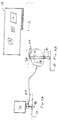
- FIG. 1 shown is a diagram illustrating a standard peripheral component interconnect (PCI) bus printed circuit board 10 having a connector 11.
- This printed circuit board 10 includes a number of components, including components shown as 12, 14, and 16.
- the component 12 is further illustrated in Figure 2A, which shows the component 12 connected to a pin 18 via conductive traces and circuitry 20.
- the conductive traces and circuitry 20 are further illustrated in Figure 2B. From the pin 18, a trace 22 extends upwards toward the component 12; from the component 12, a trace 24 extends downward toward the pin 18.
- the traces 22 and 24 could be a single trace without any intervening circuitry, but according to the invention, the circuitry 20 is included, which alternately provides for installation of a surface mount resistor 26 or a surface mount transistor 28.
- the surface mount resistor 26 has a footprint which overlaps that of the surface mount transistor 28, so the two components cannot be simultaneously installed. This is acceptable, however, because as discussed below in conjunction with Figure 3, the circuitry either requires a zero ohm resistor or a switching transistor, but not both. It will be appreciated that the conductive traces and circuitry 20 can be repeated for a plurality of the pins on the connector 11.
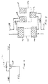
- circuitry C is shown for which the PCB layout according to the invention would be used.
- the circuit C alternatively provides for the installation of the resistor 26 or the transistor 28. If the resistor 26 is installed, it is preferably simply a short--that is, a zero ohm resistor. If the transistor 28 is installed, it is preferably a switching transistor such as a field effect transistor (FET).
- FET field effect transistor
- an address signal AD (such as from the pin 18), is directly coupled to a component address signal CAD (such as from the component 12).
- CAD such as from the component 12
- the transistor 28 is installed. In this case, a source and drain of the transistor 28 couple address and component address lines. The transistor 28 is then switched on and off by an enable signal EN, which is provided to a gate of the transistor 28.
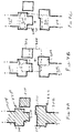
- FIG. 4 shown is a printed circuit board layout that would typically have been used to alternatively accommodate a zero ohm resistor or a switching transistor. Shown are a footprint of a surface mount zero ohm resistor 100 with two resistor pads 102 and 104. These resistor pads 102 and 104 are conductive pads etched into an insulative printed circuit board. Also shown is a footprint of a surface mount transistor 106, having three pads 108, 110, and 112. The footprints of the illustrated resistor 100 and transistor 106 correspond to a 1206 package surface mount resistor and a SOT23FT or SOT23 package surface mount transistor. These pad configurations are further illustrated below in Figures 5A and 5B, which show the pad layout 102 and 104 corresponding to the resistor 100 and the pad layout 108, 110, and 112 corresponding to the transistor 106.
- the pads 108 and 112 correspond to a source and drain of the transistor 28.
- a zero ohm resistor can be installed as the resistor 100, or a switching transistor can be installed in the transistor 106.
- the trace 114 in conjunction with the pad 102 further includes a stub 114a connected to the pad 108
- the trace 116 connected to the pad 104 further includes a trace stub 116a connected to the pad 112.
- FIG. 6 illustrated is a layout according to the invention that eliminates the stubs 114a and 116a. Shown is a first resistor pad 200 and a second resistor pad 202, which correspond to the pads 102 and 104 of Figure 4. These are conductive pads coupled to traces 204 and 206, which correspond to the traces 114 and 116. Also shown are three transistor pads 208, 210, and 212, which correspond to the pads 108, 110, and 112 of Figure 4.
- the pad 210 is electrically isolated, but provides a connection for the gate of a transistor when a transistor is installed. Also illustrated in Figure 6 are typical pad dimensions and distances associated with a 1206 resistor and a S0T23 transistor.
- Figures 7A-7C shown is an implementation of the layout of Figure 6, where the conductors as they would be laid on the printed circuit board are illustrated.
- the trace 204 connects to a small pad 220 (formed by overlapping pads 200 and 208), which does not have the stub 114a and additional pad 108 of Figure 4.
- the trace 206 connects to a small pad 222 (formed by overlapping pads 202 and 212 of Figure 7A), which again does not have the stub 116a and pad 112 of Figure 4.
- an improved printed circuit board layout is provided that reduces negative impedance characteristic and signal degradation from the traces that are necessary to allow the alternative installation of a switching transistor or a resistor. It will be appreciated that a variety of other packages can be used, so long as a portion of the footprints of pads of the transistor and the resistor overlap. This technique can be used in a variety of situations where either one or another of a component is necessary in a circuit, but not both.
- layout packages design rules checking must be overridden to allow the creation of this particular pad layout.
- layout packages require a minimum distance between various components and between traces. These distances are obviously violated, because the device envelopes actually overlap, because only one would be installed.
Landscapes
- Engineering & Computer Science (AREA)
- Microelectronics & Electronic Packaging (AREA)
- Structure Of Printed Boards (AREA)
- Electric Connection Of Electric Components To Printed Circuits (AREA)
- Semiconductor Integrated Circuits (AREA)
Applications Claiming Priority (2)
| Application Number | Priority Date | Filing Date | Title |
|---|---|---|---|
| US08/771,569 US5805428A (en) | 1996-12-20 | 1996-12-20 | Transistor/resistor printed circuit board layout |
| US771569 | 2001-01-30 |
Publications (1)
| Publication Number | Publication Date |
|---|---|
| EP0849982A1 true EP0849982A1 (en) | 1998-06-24 |
Family
ID=25092240
Family Applications (1)
| Application Number | Title | Priority Date | Filing Date |
|---|---|---|---|
| EP97310131A Withdrawn EP0849982A1 (en) | 1996-12-20 | 1997-12-16 | Improved transistor/resistor printed circuit board layout |
Country Status (3)
| Country | Link |
|---|---|
| US (1) | US5805428A (enExample) |
| EP (1) | EP0849982A1 (enExample) |
| JP (1) | JPH10190204A (enExample) |
Cited By (1)
| Publication number | Priority date | Publication date | Assignee | Title |
|---|---|---|---|---|
| ITRN20110030A1 (it) * | 2011-04-19 | 2012-10-20 | Indesit Co Spa | Dispositivo elettrico |
Families Citing this family (21)
| Publication number | Priority date | Publication date | Assignee | Title |
|---|---|---|---|---|
| US6246107B1 (en) | 1999-07-07 | 2001-06-12 | Philips Semiconductors, Inc. | Semiconductor device arrangement having configuration via adjacent bond pad coding |
| US6539449B1 (en) * | 2000-03-14 | 2003-03-25 | Intel Corporation | Capacitively loaded continuity module |
| US6985365B2 (en) * | 2001-09-28 | 2006-01-10 | Hewlett-Packard Development Company, L.P. | Topology for flexible and precise signal timing adjustment |
| US7305509B2 (en) * | 2003-03-07 | 2007-12-04 | Dell Products L.P. | Method and apparatus for zero stub serial termination capacitor of resistor mounting option in an information handling system |
| US7245501B2 (en) * | 2003-09-09 | 2007-07-17 | Hewlett-Packard Development Company, L.P. | Configurable circuit board and fabrication method |
| US7645940B2 (en) * | 2004-02-06 | 2010-01-12 | Solectron Corporation | Substrate with via and pad structures |
| CN100531516C (zh) * | 2005-07-22 | 2009-08-19 | 鸿富锦精密工业(深圳)有限公司 | 印刷电路板 |
| TWI264052B (en) * | 2005-08-19 | 2006-10-11 | Silicon Integrated Sys Corp | A switch on a package substrate for switching functions of circuit and switching method for switching functions of circuit |
| CN1942051A (zh) * | 2005-09-30 | 2007-04-04 | 鸿富锦精密工业(深圳)有限公司 | 印刷电路板的焊盘 |
| CN100544546C (zh) * | 2005-10-27 | 2009-09-23 | 鸿富锦精密工业(深圳)有限公司 | 印刷电路板 |
| US9545009B2 (en) * | 2007-05-23 | 2017-01-10 | Spectra Logic, Corporation | Passive alterable electrical component |
| CN101460007B (zh) * | 2007-12-12 | 2011-03-23 | 扬智科技股份有限公司 | 电路基板 |
| US8383952B2 (en) | 2009-08-05 | 2013-02-26 | Kovio, Inc. | Printed compatible designs and layout schemes for printed electronics |
| TWI549577B (zh) * | 2012-11-22 | 2016-09-11 | 鴻海精密工業股份有限公司 | 光纖連接器電路基板及光纖連接器 |
| TW201503768A (zh) * | 2013-07-05 | 2015-01-16 | Phison Electronics Corp | 焊墊結構及應用其之印刷電路板與記憶體儲存裝置 |
| US20150223323A1 (en) * | 2014-02-05 | 2015-08-06 | Colin Patrick O'Flynn | Footprint for Prototyping High Frequency Printed Circuit Boards |
| US9763333B2 (en) | 2015-03-09 | 2017-09-12 | Cooper Technologies Company | Shared resistor pad bypass |
| US10159151B1 (en) * | 2017-06-14 | 2018-12-18 | Unimicron Technology Corp. | Chip package circuit board module |
| CN109309269A (zh) * | 2017-07-27 | 2019-02-05 | 伊姆西Ip控股有限责任公司 | 热管理系统 |
| KR20220052395A (ko) | 2020-10-20 | 2022-04-28 | 삼성전자주식회사 | 집적 회로 및 이를 포함하는 반도체 장치 |
| US12068554B2 (en) | 2022-01-28 | 2024-08-20 | Hewlett Packard Enterprise Development Lp | Dual-path high-speed interconnect PCB layout solution |
Citations (6)
| Publication number | Priority date | Publication date | Assignee | Title |
|---|---|---|---|---|
| DE3329477A1 (de) * | 1982-11-02 | 1985-03-07 | Telefonbau Und Normalzeit Gmbh, 6000 Frankfurt | Miniatur-drahtbruecke zum herstellen von verbindungen auf baugruppen |
| JPS6351709A (ja) * | 1986-08-21 | 1988-03-04 | Matsushita Electric Ind Co Ltd | 電子回路基板 |
| JPH05102648A (ja) * | 1991-10-04 | 1993-04-23 | Hitachi Ltd | プリント基板 |
| US5266747A (en) * | 1991-08-30 | 1993-11-30 | Ford Motor Company | Minimum footprint reconfigurable input/output circuit |
| US5303122A (en) * | 1991-10-31 | 1994-04-12 | Ford Motor Company | Printed circuit board having a commonized mounting pad which different sized surface mounted devices can be mounted |
| JPH0745935A (ja) * | 1993-07-28 | 1995-02-14 | Sony Corp | プリント配線基板 |
Family Cites Families (7)
| Publication number | Priority date | Publication date | Assignee | Title |
|---|---|---|---|---|
| US3716761A (en) * | 1972-05-03 | 1973-02-13 | Microsystems Int Ltd | Universal interconnection structure for microelectronic devices |
| US4489365A (en) * | 1982-09-17 | 1984-12-18 | Burroughs Corporation | Universal leadless chip carrier mounting pad |
| FR2555011B1 (fr) * | 1983-11-15 | 1986-01-24 | Thomson Csf | Carte imprimee a empreintes |
| US5064378A (en) * | 1987-08-24 | 1991-11-12 | Zenith Data Systems Corporation | Mounting of DRAMs of different sizes and pinouts within limited footprint |
| JP3396541B2 (ja) * | 1993-08-30 | 2003-04-14 | 株式会社東芝 | 混成集積回路装置を搭載した回路基板 |
| US5557505A (en) * | 1994-07-22 | 1996-09-17 | Ast Research, Inc. | Dual pattern microprocessor package footprint |
| US5683788A (en) * | 1996-01-29 | 1997-11-04 | Dell Usa, L.P. | Apparatus for multi-component PCB mounting |
-
1996
- 1996-12-20 US US08/771,569 patent/US5805428A/en not_active Expired - Lifetime
-
1997
- 1997-12-16 EP EP97310131A patent/EP0849982A1/en not_active Withdrawn
- 1997-12-22 JP JP9353253A patent/JPH10190204A/ja active Pending
Patent Citations (6)
| Publication number | Priority date | Publication date | Assignee | Title |
|---|---|---|---|---|
| DE3329477A1 (de) * | 1982-11-02 | 1985-03-07 | Telefonbau Und Normalzeit Gmbh, 6000 Frankfurt | Miniatur-drahtbruecke zum herstellen von verbindungen auf baugruppen |
| JPS6351709A (ja) * | 1986-08-21 | 1988-03-04 | Matsushita Electric Ind Co Ltd | 電子回路基板 |
| US5266747A (en) * | 1991-08-30 | 1993-11-30 | Ford Motor Company | Minimum footprint reconfigurable input/output circuit |
| JPH05102648A (ja) * | 1991-10-04 | 1993-04-23 | Hitachi Ltd | プリント基板 |
| US5303122A (en) * | 1991-10-31 | 1994-04-12 | Ford Motor Company | Printed circuit board having a commonized mounting pad which different sized surface mounted devices can be mounted |
| JPH0745935A (ja) * | 1993-07-28 | 1995-02-14 | Sony Corp | プリント配線基板 |
Non-Patent Citations (3)
| Title |
|---|
| PATENT ABSTRACTS OF JAPAN vol. 12, no. 268 (E - 638) 27 July 1988 (1988-07-27) * |
| PATENT ABSTRACTS OF JAPAN vol. 17, no. 453 (E - 1417) 19 August 1993 (1993-08-19) * |
| PATENT ABSTRACTS OF JAPAN vol. 95, no. 5 30 June 1995 (1995-06-30) * |
Cited By (2)
| Publication number | Priority date | Publication date | Assignee | Title |
|---|---|---|---|---|
| ITRN20110030A1 (it) * | 2011-04-19 | 2012-10-20 | Indesit Co Spa | Dispositivo elettrico |
| WO2012143873A1 (en) * | 2011-04-19 | 2012-10-26 | Indesit Company S.P.A. | Electrical device |
Also Published As
| Publication number | Publication date |
|---|---|
| JPH10190204A (ja) | 1998-07-21 |
| US5805428A (en) | 1998-09-08 |
Similar Documents
| Publication | Publication Date | Title |
|---|---|---|
| US5805428A (en) | Transistor/resistor printed circuit board layout | |
| US6236572B1 (en) | Controlled impedance bus and method for a computer system | |
| US4600256A (en) | Condensed profile electrical connector | |
| US5986893A (en) | Apparatus for controlling the impedance of high speed signals on a printed circuit board | |
| KR100290445B1 (ko) | 메모리모듈과 이 메모리모듈이 삽입되는 소켓 | |
| JP2001160663A (ja) | 回路基板 | |
| US8201133B2 (en) | Printed circuit board with reduced signal distortion | |
| US20060141854A1 (en) | Printed circuit board | |
| US5184284A (en) | Method and apparatus for implementing engineering changes for integrated circuit module | |
| US20040090757A1 (en) | Printed circuit board | |
| US6840808B2 (en) | Connector for a plurality of switching assemblies with compatible interfaces | |
| US6930888B2 (en) | Mechanism to cross high-speed differential pairs | |
| US6477060B1 (en) | Dual channel bus routing using asymmetric striplines | |
| CN1179608C (zh) | 印刷线路板及具有该印刷线路板的电子设备 | |
| US12068554B2 (en) | Dual-path high-speed interconnect PCB layout solution | |
| US5519584A (en) | Laminated cylindrical backplane | |
| KR100511405B1 (ko) | 고속 버스 접속 시스템 | |
| US6495911B1 (en) | Scalable high frequency integrated circuit package | |
| US7269028B2 (en) | Trace-pad interface for improved signal quality | |
| US20070075418A1 (en) | Emi shielding device for pcb | |
| CN217936051U (zh) | 仪表pcb板及电动车仪表 | |
| JPH0555719A (ja) | 回路基板装置 | |
| JPH04324920A (ja) | 表面実装部品の実装方法 | |
| US7186922B2 (en) | Circuit board | |
| JP4258168B2 (ja) | マザーボード |
Legal Events
| Date | Code | Title | Description |
|---|---|---|---|
| PUAI | Public reference made under article 153(3) epc to a published international application that has entered the european phase |
Free format text: ORIGINAL CODE: 0009012 |
|
| AK | Designated contracting states |
Kind code of ref document: A1 Designated state(s): DE FR GB IT |
|
| AX | Request for extension of the european patent |
Free format text: AL;LT;LV;MK;RO;SI |
|
| 17P | Request for examination filed |
Effective date: 19981221 |
|
| AKX | Designation fees paid |
Free format text: DE FR GB IT |
|
| RBV | Designated contracting states (corrected) |
Designated state(s): DE FR GB IT |
|
| 17Q | First examination report despatched |
Effective date: 20031111 |
|
| STAA | Information on the status of an ep patent application or granted ep patent |
Free format text: STATUS: THE APPLICATION IS DEEMED TO BE WITHDRAWN |
|
| 18D | Application deemed to be withdrawn |
Effective date: 20060701 |