EP0848842B2 - Uhrwerk - Google Patents
Uhrwerk Download PDFInfo
- Publication number
- EP0848842B2 EP0848842B2 EP96923940A EP96923940A EP0848842B2 EP 0848842 B2 EP0848842 B2 EP 0848842B2 EP 96923940 A EP96923940 A EP 96923940A EP 96923940 A EP96923940 A EP 96923940A EP 0848842 B2 EP0848842 B2 EP 0848842B2
- Authority
- EP
- European Patent Office
- Prior art keywords
- circuit
- generator
- capacitive component
- timepiece movement
- voltage
- Prior art date
- Legal status (The legal status is an assumption and is not a legal conclusion. Google has not performed a legal analysis and makes no representation as to the accuracy of the status listed.)
- Expired - Lifetime
Links
Images


Classifications
-
- G—PHYSICS
- G04—HOROLOGY
- G04C—ELECTROMECHANICAL CLOCKS OR WATCHES
- G04C10/00—Arrangements of electric power supplies in time pieces
-
- G—PHYSICS
- G04—HOROLOGY
- G04C—ELECTROMECHANICAL CLOCKS OR WATCHES
- G04C11/00—Synchronisation of independently-driven clocks
Definitions
- the invention relates to a movement according to the preamble of patent claim 1.
- the spring via a gear train a time display and a generator supplying an AC voltage.
- the generator feeds a voltage converter circuit
- the voltage converter circuit feeds a capacitive component
- the capacitive component feeds a reference electronic circuit having a stable oscillator and an electronic control circuit.
- the electronic control circuit comprises a comparator logic circuit and an energy dissipation circuit connected to an output of the comparator logic circuit and controllable by the comparator logic circuit in its power consumption.
- One input of the comparator logic shaft is connected to the electronic reference circuit and another input of the comparator logic circuit is connected to the generator via a comparator stage and an auto-coincidence circuit.
- the comparator logic circuit is adapted to compare a clock signal from the electronic reference circuit with a clock signal from the generator, and controls the magnitude of the power consumption of the electronic control circuit over the amount of power consumption of the energy dissipation circuit, depending on the result of this comparison this way, via the control of the control circuit power consumption regulates the gear of the generator and thus the course of the time display.
- the power consumption of the Energy dissipationsscnies in the known from CH-597 636 clockwork is controlled by the comparator logic circuit according to CH-597 636, however, only in two stages. Namely, the power consumption of the energy dissipation circuit according to CH-597 636 is either maximum or zero. This means that the generator can either be braked only with maximum strength or not at all. This results in considerable control oscillations in the gear regulation of the movement. On this catfish results in a relatively poor energetic efficiency of the movement.
- the voltage converter circuit according to CH-597 636 is a rectifier.
- Diodes are commonly used in the watch-making technique for rectification, for example, as disclosed in GB-A-2,158,274, EP-A-0,326,312, US-A-4,653,931, EP-A-0,467,667, EP-A-0,326,313, EP-A -0,309,164, EP-A-0,241,219 and EP-A-0,679,968.
- Diodes are passive components. The use of diodes as a rectifier during the entire life of a clockwork affected due to the diode threshold voltage, the energetic efficiency of the movement. Fermer is referred to EP-A-0,695,978.
- General technical background, which is not relevant in the present context, is given by JP-A-58-179379. Of relevance in the present context, however, is EP-B-0,157,789.
- the required drive power consists of the mechanical drive power for the movement, the friction power and the electrical power of the generator.
- the electric power output of the generator is determined by the power consumption of an energy-consuming electronic circuit connected to the generator. It should also be noted that the frictional loss of the generator is directly related to the voltage induced by the generator. As a rough estimate is that the mass of a rotor of the generator must be higher, the higher the induced voltage should be.
- the invention has for its object to provide a clock, the spring via a gear train a time display and a generator supplying an AC voltage and can be operated in energetically particularly favorable manner.
- control oscillations can be reduced and in this way energy losses associated with the control oscillations can be reduced.
- the power consumption of the electronic control circuit in a predetermined size range is even substantially steplessly controlled. This is a comparison with the clockwork according to the CH-597 636 significant reduction in the control vibrations and related significant improvement in the energy efficiency of the movement given.
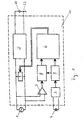
- FIG. 1 an electronic part of a movement according to the invention is shown as a block diagram.
- a generator 1 supplying an alternating voltage is connected via an unillustrated gear train to a spring, also not shown.
- the spring drives the generator 1 and a time display, not shown.
- the nominal frequency of the AC voltage of the generator 1 is advantageously 2 n Hz, where n is a non-zero natural number.
- the mechanical part of the movement according to the invention is state of the art. Reference is made in this regard to CH-597 636.
- the voltage source circuit 2 feeds a first capacitive component 10.
- the first capacitive component 10 supplies an electronic reference circuit 3, 4, 5 with a stable oscillator 3, 4 and an electronic control circuit 6, 7, 8, 9
- the stable oscillator 3, 4 has a quartz crystal 4 whose oscillation defines a reference frequency.
- the voltage converter circuit 2, the electronic control circuit 6, 7, 8, 9 and the electronic reference circuit 3, 5 with the exception of the quartz crystal 4 and with the exception of all the capacitive components present in said circuits are constructed as an IC 11. In another embodiment, even the capacitive components are integrated into the IC 11.
- the electronic control circuit 6, 7, 8, 9 has a comparator logic circuit 6, whose one input to the electronic reference circuit 3, 4, 5 and the other input via a zero crossing of the AC voltage detecting comparator stage 7 and an anti-coincidence circuit 8 with connected to the generator 1.
- the anti-coincidence circuit 8 is essentially a latch which prevents simultaneous input of pulses on both inputs of the comparator logic circuit 6.
- the electronic control circuit 6, 7, 8, 9 has a connected to an output of the comparator logic circuit 6 and controllable by the comparator logic circuit 6 in their power consumption Energydissipationsscrien 9.
- the energy dissipation circuit 9 is made up of a large number of identical ohmic resistors.
- the size of an ohmic resistor is small in comparison with the magnitude of the resistance that results when all the ohmic resistances in series are connected in series.
- the comparator logic circuit 6 controls the power consumption of the energy dissipation circuit 9 by counting a number of changed in the current path connected ohmic resistors. In this way, the power consumption of the electronic control circuit 6, 7, 8, 9 in a predetermined by the number of resistors size range is controlled substantially continuously.
- the energy dissipation circuit 9 is also possible to construct the energy dissipation circuit 9 as a controllable current source.
- the comparator logic circuit 6 compares a coming from the electronic reference circuit 3, 4, 5 clock signal with a derived from the generator 1 clock signal. Depending on the result of this comparison, the comparator logic circuit 6 controls the amount of power consumption of the electronic control circuit 6, 7, 8, 9 over the amount of power consumption of the Energydissipationsscrien 9. In this way, via the control of the control circuit power consumption of the gear of the generator 1 and thus the course of the time display regulated.
- the control is designed so that the gear of the time display is synchronized in the desired manner with the reference frequency supplied by the quartz crystal 4.
- the comparator logic circuit 6 has a counter whose count corresponds to a gear difference between the generator 1 and the electronic reference circuit 3, 4, 5.
- the power consumption of the Energydissipationsscnies 9 is controlled in dependence on the count of the counter. Depending on the state of the counter 9 more or less energy is dissipated in the Energydissipationsscnies and thus the generator 1 more or less charged. Each count is associated with a predetermined effective resistance combination in the Energydissipationsscnies 9.
- the comparator logic circuit 6, depending on the count can switch on or off the active current path, the ohmic resistances present in the energy dissipation circuit 9 individually and in various combinations in the active current path. In this case, of course, the case is provided that is switched at one or more counter readings none of said ohmic resistors in the active current path.
- the control is limited by the fact that on reaching a certain maximum level of the counter counting of generator pulses is interrupted. This is particularly necessary to ensure trouble-free starting of all electronic components of the movement in the event that the spring is first re-opened after a complete stop of the movement.
- a similar effect is achieved if the comparator logic circuit 6 and the Energydissipationsschaftung 9 so coordinated that the power consumption of the Energydissipationsscaria 9 for a predetermined Zahlerstands Scheme (eg 0 to 16) is kept minimal and linear when exceeding the predetermined meter reading range changes proportionally to the meter reading.
- control can be interrupted at a certain low level of the counter and a counting of pulses.
- the movement also has a device, not shown, for displaying the power reserve as a function of the count.
- the power reserve is displayed by means of an LCD.
- the electronic reference circuit 3, 4, 5 has a frequency divider circuit 5 connected between the stable oscillator 3, 4 and the connection to the electronic control circuit 6, 7, 8, 9. This divides the supplied from the quartz crystal 4 reference frequency in a defined manner to allow easier synchronization of the time display.
- the voltage converter circuit 2 fulfills both a rectifier function and a voltage tripler function.
- a first diode 14 is connected in series with the generator 1 and with the first capacitive component 10.
- a first switch 19 is connected in parallel with the first diode 14, but in series with the generator 1 and in series with the first capacitive component 10. The first switch 19 is actively controlled by a first comparator 21.
- the voltage converter circuit further comprises a voltage tripler circuit 12, 13, 15, 16, 17, 18, 20, 23, the input side to the generator 1 and the load side to the first capacitive element 10 and to the parallel connection of the first diode 14 and the first switch 19th is coupled.
- a load-side connection of the voltage tripler circuit 12, 13, 15, 16, 17, 18, 20, 23 opens together with the terminal of the first capacitive component 10 facing away from the first diode 14 into a ground node 22.
- the first comparator 21 compares the electrical potential at the terminal of the first capacitive component 10, which is not at ground potential, with the electrical potential of the non-ground potential load-side terminal of the voltage tripler circuit 12, 13, 15, 16, 17, 18, 20, 23.
- the first switch 19 is closed by the first comparator 21 only when the voltage of the first capacitive element 10 for operating the first comparator 21 is sufficient and the electric potential the ground-free load-side terminal of the voltage trip circuit 12, 13, 15, 16, 17, 18, 20, 23 is high enough for further charging of the first capacitive element 10.
- the first switch 19 is a first field-effect transistor and connected so that in its locked state, a part of its structure acts as a first diode 14.
- the spring, the gear train, the generator 1, the voltage converter circuit 2 and the electronic control circuit 6, 7, 8, 9 are designed so that the generator 1 immediately after a start of the movement until the time of charging of the first capacitive element 10 on the predetermined value operates at a speed which is greater than the target speed of the generator 1. In this case, charging of the first capacitive component 10 takes place via the first diode 14.
- the voltage value of the first capacitive component 10 which is sufficient for operating the first comparator 21 and for operating a second comparator 20 present in the voltage tripler circuit 12, 13, 15, 16, 17, 18, 20, 23 and explained in more detail below is shown in FIG 0.6 V.
- the voltage drop across the first diode 14 is 400 mV.
- the first comparator 21 closes, as soon as the voltage supplied by the voltage tripler circuit 12, 13, 15, 16, 17, 18, 20, 23 is higher than the voltage of the first capacitive element 10, the first switch 19, i. he opens the first field effect transistor.
- the voltage drop across the channel of the first field effect transistor is only 10 mV. The voltage loss is thus significantly reduced.
- the first comparator 21 closes the first field effect transistor. If the voltage supplied by the voltage tripler circuit 12, 13, 15, 16, 17, 18, 20, 23 again increases to a sufficiently large value, the first comparator 21 opens the first field-effect transistor again and so on. The charging of the first capacitive element 10 thus takes place only in the start-up phase of the movement on the afflicted with a highchrosveriust first diode 14.
- the voltage converter circuit 2 in addition to its rectifier function must also fulfill aaasvervielfacherfunktion, including the already mentioned,tosvervielfacherscaria 12, 13, 15, 16, 17, 18, 20, 23 is used.
- the voltage multiplier circuit 12, 13, 15, 16, 17, 18, 20, 23 is a voltage tripler circuit. Two different embodiments of the voltage tripler circuit are shown in FIGS.
- a first embodiment of the voltage tripler circuit (see FIG. 2) further comprises a parallel connection of a second diode 12 and a second switch 17 and a parallel connection of a third diode 23 and a third switch 18.
- the parallel connection of the second diode 12 and the second switch 17 is connected in series between the generator-side terminal of the second capacitive component 15 and the load-side terminal of the third capacitive component 16.
- the parallel connection of the third diode 23 and the third switch 18 is connected in series between the generator-side terminal of the third capacitive element 16 and the load-side terminal of the second capacitive element 15.
- the first embodiment of the voltage tripler circuit also has a fourth diode 13 connected in series between the load-side terminals of the second and third capacitive components 15, 16 ,
- the second, the third and the fourth diode 12, 23, 13 are connected in the same forward direction, and the first diode 14 is connected in the opposite direction of passage.
- the second comparator 20 compares the electrical potential at the connected to the second capacitive element 15 terminal of the generator 1 with the electrical potential at the load-side terminal of the third capacitive element 16.
- the second and / or the third switch 17, 18 is through the second comparator 20 closed only when the voltage of the first capacitive Component 10 is sufficient for operating the second comparator 20 and provided by the generator 1 available electrical potential for charging the second and the third capacitive element 15, 16 is high enough.
- the second switch 17 is a second field effect transistor
- the third switch 18 is a third field effect transistor.
- the second field effect transistor is connected so that in its locked state, part of its structure acts as a second diode 12.
- the third field effect transistor is switched so that in its locked state, a part of its structure acts as a third diode 23.
- the second field effect transistor and the third field effect transistor are initially blocked.
- the charging of the second capacitive component 15 and of the third capacitive component 16 takes place via the second, third and fourth diode 12, 23, 13.
- the second comparator 20 opens the second field effect transistor and the third field effect transistor.
- the charging of the second and the third capacitive component 15, 16 now takes place via the second field effect transistor and the third field effect transistor.
- the reduction of the voltage losses is analogous to the above-described reduction of the voltage loss during the transition from the first diode 14 to the first field effect transistor.
- the opening and closing of the second and the third field effect transistor by the second comparator 20 In an analogous manner, the opening and closing of the second and the third field effect transistor by the second comparator 20. If the voltage supplied by the generator 1 falls below the voltage of the third capacitive element 16, the second comparator 20 blocks the second and the third field effect transistor , As the voltage supplied by the generator 1 increases above the voltage of the third capacitive device 16, the second and third field effect transistors are opened, i. the second and third switches 17, 18 are closed. Compared to pure diode use thus results in the dosesverdreifachersciens a more economical use of the energy reserve of the movement, whereby the power reserve is increased.
- FIG. 3 shows a second embodiment of the voltage tripler circuit in which, unlike the first embodiment of the voltage tripler circuit, the circuit branch containing the fourth diode 13 is missing. Since the fourth diode 13 is not absolutely necessary for the operation of the voltage tripler circuit, the second embodiment of the voltage tripler circuit also ensures reliable operation of the voltage converter circuit 2. Of course, the respective existing diodes always have to be suitably adapted to the current circuit environment in their dimensioning. The same applies to the third embodiment of the voltage tripler circuit shown in FIG. 4, which has only the circuit branch with the fourth diode 13, but not the circuit branches with the second diode 12 and the third diode 23.
- the second switch 17 occurs alone or in the fourth embodiment of the voltage tripler circuit third switch 18 alone.
- the voltage converter circuit 2 and the electronic control circuit 6, 7, 8, 9 are tuned such that the power consumption of the Energydissipationsscrien 9 assumes a minimum value while any of the capacitive devices 10, 15, 16 is charged.
- the voltage converter circuit 2 and the electronic control circuit 6, 7, 8, 9 are designed so that the power consumption of the Energydissipationsscrien 9 at intervals of 3 x 10 -2 s regularly for 5 x 10 -4 s assumes a minimum value to the comparators 20th , 21 to allow a potential comparison according to their function. If the potential comparison were carried out at a generator load that is above the minimum load of the generator 1, then the comparators 20, 21 with respect to the charging possibilities of the capacitive components 10, 15, 16 would come to wrong conclusions, because they would be compared to the generator voltage at minimum load detect reduced generator voltage.
Landscapes
- Physics & Mathematics (AREA)
- General Physics & Mathematics (AREA)
- Engineering & Computer Science (AREA)
- Power Engineering (AREA)
- Electromechanical Clocks (AREA)
- Electric Clocks (AREA)
- Lubrication Of Internal Combustion Engines (AREA)
- Control Of Eletrric Generators (AREA)
- Magnetic Heads (AREA)
Applications Claiming Priority (3)
| Application Number | Priority Date | Filing Date | Title |
|---|---|---|---|
| CH254595 | 1995-09-07 | ||
| CH2545/95 | 1995-09-07 | ||
| PCT/EP1996/002791 WO1997009657A1 (de) | 1995-09-07 | 1996-06-26 | Uhrwerk |
Publications (3)
| Publication Number | Publication Date |
|---|---|
| EP0848842A1 EP0848842A1 (de) | 1998-06-24 |
| EP0848842B1 EP0848842B1 (de) | 1999-04-28 |
| EP0848842B2 true EP0848842B2 (de) | 2006-04-19 |
Family
ID=4236210
Family Applications (1)
| Application Number | Title | Priority Date | Filing Date |
|---|---|---|---|
| EP96923940A Expired - Lifetime EP0848842B2 (de) | 1995-09-07 | 1996-06-26 | Uhrwerk |
Country Status (10)
| Country | Link |
|---|---|
| US (1) | US5881027A (zh) |
| EP (1) | EP0848842B2 (zh) |
| JP (2) | JPH11502024A (zh) |
| CN (3) | CN1246743C (zh) |
| AT (1) | ATE179529T1 (zh) |
| DE (1) | DE59601785D1 (zh) |
| ES (1) | ES2132931T5 (zh) |
| GR (1) | GR3030192T3 (zh) |
| HK (1) | HK1012204A1 (zh) |
| WO (1) | WO1997009657A1 (zh) |
Families Citing this family (12)
| Publication number | Priority date | Publication date | Assignee | Title |
|---|---|---|---|---|
| US6169709B1 (en) * | 1995-09-07 | 2001-01-02 | Konrad Schafroth | Watch movement |
| DK0848842T3 (da) * | 1996-06-26 | 1999-11-08 | Konrad Schafroth | Urværk |
| US6421261B1 (en) | 1996-11-13 | 2002-07-16 | Seiko Epson Corporation | Power supply apparatus with unidirectional units |
| US6795378B2 (en) | 1997-09-30 | 2004-09-21 | Seiko Epson Corporation | Electronic device, electronically controlled mechanical timepiece, and control method therefor |
| US6041021A (en) * | 1997-09-30 | 2000-03-21 | Seiko Epson Corporation | Electronically controlled mechanical timepiece and control method therefor |
| US6314059B1 (en) * | 1997-09-30 | 2001-11-06 | Seiko Epson Corporation | Electronically controlled, mechanical timepiece and control method for the same |
| US6477116B1 (en) * | 1997-09-30 | 2002-11-05 | Seiko Epson Corporation | Rotation controller and rotation control method |
| CN100399217C (zh) | 1999-03-03 | 2008-07-02 | 精工爱普生株式会社 | 电子设备及其控制方法 |
| CH694621A5 (fr) | 2001-07-02 | 2005-04-29 | Richemont Int Sa | Procédé de régulation et module électronique de régulation pour mouvement d'horlogerie à remontage mécanique. |
| US7252679B2 (en) * | 2001-09-13 | 2007-08-07 | Cordis Corporation | Stent with angulated struts |
| EP2561409B1 (de) * | 2010-04-21 | 2019-08-28 | Team Smartfish GmbH | Regelorgan für ein uhrwerk, und entsprechendes verfahren |
| JP6232705B2 (ja) * | 2013-02-04 | 2017-11-22 | セイコーエプソン株式会社 | 電子制御式機械時計 |
Citations (13)
| Publication number | Priority date | Publication date | Assignee | Title |
|---|---|---|---|---|
| DE2402603A1 (de) † | 1974-01-19 | 1975-07-24 | Hubert Kalinowski | Anordnung zum spannungsvervielfacher |
| US3937001A (en) † | 1972-11-21 | 1976-02-10 | Berney Jean Claude | Watch movement driven by a spring and regulated by an electronic circuit |
| JPS5482039A (en) † | 1977-12-12 | 1979-06-29 | Seiko Instr & Electronics | Circuit for charging solar cell and secondary cell |
| WO1985001161A1 (en) † | 1983-09-02 | 1985-03-14 | American Telephone & Telegraph Company | Improvements in or relating to rectifier circuits |
| JPS63190562A (ja) † | 1987-01-29 | 1988-08-08 | Nec Corp | 倍電圧整流回路 |
| DE3906861A1 (de) † | 1988-03-04 | 1989-09-14 | Fraunhofer Ges Forschung | Energieversorgungseinheit |
| DE3834867C1 (en) † | 1988-10-13 | 1990-01-25 | Telenorma Telefonbau Und Normalzeit Gmbh, 6000 Frankfurt, De | Circuit arrangement for the parallel connection of power supply devices |
| JPH0345158A (ja) † | 1989-07-12 | 1991-02-26 | Seiko Epson Corp | 回転動力調速装置 |
| US5001685A (en) † | 1988-01-25 | 1991-03-19 | Seiko Epson Corporation | Electronic wristwatch with generator |
| JPH0365057A (ja) † | 1989-08-02 | 1991-03-20 | Nec Corp | 3倍電圧整流回路 |
| JPH077928A (ja) † | 1993-06-15 | 1995-01-10 | Fuji Electric Co Ltd | 同期整流用パワ−mosfetの制御装置 |
| EP0665634A1 (de) † | 1994-01-31 | 1995-08-02 | Siemens Aktiengesellschaft | Schaltungsanordnung mit einem Feldeffekttransistor |
| EP0870357A1 (en) † | 1995-12-29 | 1998-10-14 | EM Microelectronic-Marin SA | Active rectifier having minimal energy losses |
Family Cites Families (6)
| Publication number | Priority date | Publication date | Assignee | Title |
|---|---|---|---|---|
| JPS5367826A (en) * | 1976-11-29 | 1978-06-16 | Seiko Epson Corp | Boosting circuit |
| CH665082GA3 (zh) * | 1986-03-26 | 1988-04-29 | ||
| CH686332B5 (fr) * | 1994-04-25 | 1996-09-13 | Asulab Sa | Pièce d'horlogerie mué par une source d'énergie mécanique et régulée par un circuit électronique. |
| CH688879B5 (fr) * | 1995-08-10 | 1998-11-13 | Asulab Sa | Pièce d'horlogerie avec indication de la réserve de marche. |
| FR2748583B1 (fr) * | 1996-05-07 | 1998-06-26 | Asulab Sa | Stabilisation d'un circuit electronique de regulation du mouvement mecanique d'une piece d'horlogerie |
| FR2752070B1 (fr) * | 1996-08-01 | 1998-09-18 | Asulab Sa | Piece d'horlogerie electronique comportant une generatrice entrainee par un barillet a ressort |
-
1996
- 1996-06-26 EP EP96923940A patent/EP0848842B2/de not_active Expired - Lifetime
- 1996-06-26 CN CNB031014518A patent/CN1246743C/zh not_active Expired - Fee Related
- 1996-06-26 AT AT96923940T patent/ATE179529T1/de not_active IP Right Cessation
- 1996-06-26 WO PCT/EP1996/002791 patent/WO1997009657A1/de active IP Right Grant
- 1996-06-26 DE DE59601785T patent/DE59601785D1/de not_active Expired - Lifetime
- 1996-06-26 US US09/029,455 patent/US5881027A/en not_active Expired - Fee Related
- 1996-06-26 CN CN96196745A patent/CN1119720C/zh not_active Expired - Fee Related
- 1996-06-26 JP JP9510793A patent/JPH11502024A/ja active Pending
- 1996-06-26 CN CNB03101450XA patent/CN1235100C/zh not_active Expired - Fee Related
- 1996-06-26 ES ES96923940T patent/ES2132931T5/es not_active Expired - Lifetime
-
1998
- 1998-12-15 HK HK98113389A patent/HK1012204A1/xx not_active IP Right Cessation
-
1999
- 1999-05-11 GR GR990401281T patent/GR3030192T3/el unknown
-
2002
- 2002-05-17 JP JP2002142765A patent/JP3485557B2/ja not_active Expired - Fee Related
Patent Citations (13)
| Publication number | Priority date | Publication date | Assignee | Title |
|---|---|---|---|---|
| US3937001A (en) † | 1972-11-21 | 1976-02-10 | Berney Jean Claude | Watch movement driven by a spring and regulated by an electronic circuit |
| DE2402603A1 (de) † | 1974-01-19 | 1975-07-24 | Hubert Kalinowski | Anordnung zum spannungsvervielfacher |
| JPS5482039A (en) † | 1977-12-12 | 1979-06-29 | Seiko Instr & Electronics | Circuit for charging solar cell and secondary cell |
| WO1985001161A1 (en) † | 1983-09-02 | 1985-03-14 | American Telephone & Telegraph Company | Improvements in or relating to rectifier circuits |
| JPS63190562A (ja) † | 1987-01-29 | 1988-08-08 | Nec Corp | 倍電圧整流回路 |
| US5001685A (en) † | 1988-01-25 | 1991-03-19 | Seiko Epson Corporation | Electronic wristwatch with generator |
| DE3906861A1 (de) † | 1988-03-04 | 1989-09-14 | Fraunhofer Ges Forschung | Energieversorgungseinheit |
| DE3834867C1 (en) † | 1988-10-13 | 1990-01-25 | Telenorma Telefonbau Und Normalzeit Gmbh, 6000 Frankfurt, De | Circuit arrangement for the parallel connection of power supply devices |
| JPH0345158A (ja) † | 1989-07-12 | 1991-02-26 | Seiko Epson Corp | 回転動力調速装置 |
| JPH0365057A (ja) † | 1989-08-02 | 1991-03-20 | Nec Corp | 3倍電圧整流回路 |
| JPH077928A (ja) † | 1993-06-15 | 1995-01-10 | Fuji Electric Co Ltd | 同期整流用パワ−mosfetの制御装置 |
| EP0665634A1 (de) † | 1994-01-31 | 1995-08-02 | Siemens Aktiengesellschaft | Schaltungsanordnung mit einem Feldeffekttransistor |
| EP0870357A1 (en) † | 1995-12-29 | 1998-10-14 | EM Microelectronic-Marin SA | Active rectifier having minimal energy losses |
Also Published As
| Publication number | Publication date |
|---|---|
| EP0848842B1 (de) | 1999-04-28 |
| CN1246743C (zh) | 2006-03-22 |
| ES2132931T3 (es) | 1999-08-16 |
| CN1119720C (zh) | 2003-08-27 |
| EP0848842A1 (de) | 1998-06-24 |
| JP2003028970A (ja) | 2003-01-29 |
| HK1012204A1 (en) | 1999-07-30 |
| CN1235100C (zh) | 2006-01-04 |
| DE59601785D1 (de) | 1999-06-02 |
| JPH11502024A (ja) | 1999-02-16 |
| CN1195408A (zh) | 1998-10-07 |
| WO1997009657A1 (de) | 1997-03-13 |
| CN1441332A (zh) | 2003-09-10 |
| US5881027A (en) | 1999-03-09 |
| JP3485557B2 (ja) | 2004-01-13 |
| ES2132931T5 (es) | 2006-11-16 |
| ATE179529T1 (de) | 1999-05-15 |
| CN1441331A (zh) | 2003-09-10 |
| GR3030192T3 (en) | 1999-08-31 |
Similar Documents
| Publication | Publication Date | Title |
|---|---|---|
| EP0848842B2 (de) | Uhrwerk | |
| DE2357244C3 (de) | Mechanisches Uhrwerk, dessen Ganggenauigkeit von einer elektronischen Schaltung bestimmt wird | |
| EP0432386A1 (de) | Anordnung zur Ermittlung von Werten elektrischer Grössen, die von Messwerten mindestens zweier elektrischer Eingangsgrössen der Anordnung ableitbar sind | |
| DE2619714A1 (de) | Vorrichtung zum steuern von wechselstrommotoren | |
| EP2043243A1 (de) | Umrichterschaltung sowie Verfahren zum Betrieb einer solchen Umrichterschaltung | |
| DE2305251B2 (de) | Erreger-einrichtung fuer einen selbsterregten asynchron-generator | |
| EP0594670B1 (de) | Vorrichtung zur erzeugung von schwingungen und deren anwendung | |
| DE3823038C2 (de) | Verfahren zur Überwachung des Ladezustandes einer Batterie | |
| EP0152739A1 (de) | Verfahren zur Ermittlung des Zeitpunktes der Wiedereinschaltung eines Leistungsschalters und Gerät zur Durchführung dieses Verfahrens | |
| DE2838834A1 (de) | Digital abstimmbarer integrierter impulsgenerator mit abstimmsystem | |
| DE19703645A1 (de) | Vorrichtung und Verfahren zum Erzeugen von Vorspannungen für eine Flüssigkristallanzeige | |
| DE2605385A1 (de) | Motorantriebssystem und schaltungsanordnung fuer ein motorantriebssystem | |
| DE2233800B2 (de) | Schaltung zur geringfügigen Erhöhung der Ausgangsfrequenz eines von einem Schwingkristall angetriebenen Impulsgenerators für eine zeitanzeigende Einrichtung | |
| DE2621532A1 (de) | Verfahren zur frequenzsteuerung von elektrischen schwingungssignalen und frequenznormal-schaltungen fuer elektrische uhren | |
| DE2649096A1 (de) | Vorrichtung zur ermittlung von ermuedungsschaeden an turbinen | |
| DE2831950A1 (de) | Steuerschaltung und steuersystem fuer eine maschine | |
| DE2744798C3 (de) | Elektromechanische Kalenderuhr | |
| EP0026869A1 (de) | Wartungs-Überwachungseinrichtung für eine Anlage | |
| DE2748400A1 (de) | Anzeigegeraet | |
| DE2741205A1 (de) | Dynamisches cmos-schnell-flip-flop- system | |
| DE2826518A1 (de) | Steuerkreis fuer eine maschine | |
| WO2011151103A1 (de) | Schaltung zur taktung eines fpga | |
| DE69839389T2 (de) | Elektronisches Uhrwerk, mit von einer Zugfeder angetriebenem Generator | |
| EP1246351A2 (de) | Schaltungsanordnung zur Gewinnung einer Gleichspannung | |
| DE2558526A1 (de) | Verfahren zur ueberwachung des ladezustandes einer batterie und vorrichtung zur durchfuehrung dieses verfahrens |
Legal Events
| Date | Code | Title | Description |
|---|---|---|---|
| PUAI | Public reference made under article 153(3) epc to a published international application that has entered the european phase |
Free format text: ORIGINAL CODE: 0009012 |
|
| 17P | Request for examination filed |
Effective date: 19980218 |
|
| AK | Designated contracting states |
Kind code of ref document: A1 Designated state(s): AT BE CH DE DK ES FI FR GB GR IE IT LI LU MC NL PT SE |
|
| GRAG | Despatch of communication of intention to grant |
Free format text: ORIGINAL CODE: EPIDOS AGRA |
|
| 17Q | First examination report despatched |
Effective date: 19981022 |
|
| RBV | Designated contracting states (corrected) |
Designated state(s): AT BE CH DE DK ES FI FR GB GR IE IT LI LU MC NL PT SE |
|
| GRAG | Despatch of communication of intention to grant |
Free format text: ORIGINAL CODE: EPIDOS AGRA |
|
| GRAH | Despatch of communication of intention to grant a patent |
Free format text: ORIGINAL CODE: EPIDOS IGRA |
|
| GRAH | Despatch of communication of intention to grant a patent |
Free format text: ORIGINAL CODE: EPIDOS IGRA |
|
| RAP1 | Party data changed (applicant data changed or rights of an application transferred) |
Owner name: SCHAFROTH, KONRAD |
|
| GRAA | (expected) grant |
Free format text: ORIGINAL CODE: 0009210 |
|
| AK | Designated contracting states |
Kind code of ref document: B1 Designated state(s): AT BE CH DE DK ES FI FR GB GR IE IT LI LU MC NL PT SE |
|
| REF | Corresponds to: |
Ref document number: 179529 Country of ref document: AT Date of ref document: 19990515 Kind code of ref document: T |
|
| REG | Reference to a national code |
Ref country code: CH Ref legal event code: NV Representative=s name: ISLER & PEDRAZZINI AG Ref country code: CH Ref legal event code: EP |
|
| ITF | It: translation for a ep patent filed |
Owner name: BUGNION S.P.A. |
|
| REG | Reference to a national code |
Ref country code: IE Ref legal event code: FG4D Free format text: GERMAN |
|
| REF | Corresponds to: |
Ref document number: 59601785 Country of ref document: DE Date of ref document: 19990602 |
|
| GBT | Gb: translation of ep patent filed (gb section 77(6)(a)/1977) |
Effective date: 19990524 |
|
| REG | Reference to a national code |
Ref country code: ES Ref legal event code: FG2A Ref document number: 2132931 Country of ref document: ES Kind code of ref document: T3 |
|
| ET | Fr: translation filed | ||
| REG | Reference to a national code |
Ref country code: PT Ref legal event code: SC4A Free format text: AVAILABILITY OF NATIONAL TRANSLATION Effective date: 19990519 |
|
| REG | Reference to a national code |
Ref country code: DK Ref legal event code: T3 |
|
| PLBQ | Unpublished change to opponent data |
Free format text: ORIGINAL CODE: EPIDOS OPPO |
|
| PLBI | Opposition filed |
Free format text: ORIGINAL CODE: 0009260 |
|
| PLBF | Reply of patent proprietor to notice(s) of opposition |
Free format text: ORIGINAL CODE: EPIDOS OBSO |
|
| 26 | Opposition filed |
Opponent name: A.W. KOCH UNIV.-PROF. DR.-ING. Effective date: 20000128 Opponent name: DEREK GAMBELL Effective date: 20000128 Opponent name: ETA SA FABRIQUES D'EBAUCHES Effective date: 20000128 |
|
| NLR1 | Nl: opposition has been filed with the epo |
Opponent name: A.W. KOCH UNIV.-PROF. DR.-ING. Opponent name: DEREK GAMBELL Opponent name: ETA SA FABRIQUES D'EBAUCHES |
|
| PLBF | Reply of patent proprietor to notice(s) of opposition |
Free format text: ORIGINAL CODE: EPIDOS OBSO |
|
| PLBF | Reply of patent proprietor to notice(s) of opposition |
Free format text: ORIGINAL CODE: EPIDOS OBSO |
|
| REG | Reference to a national code |
Ref country code: GB Ref legal event code: IF02 |
|
| REG | Reference to a national code |
Ref country code: CH Ref legal event code: PUE Owner name: SCHAFROTH, KONRAD TRANSFER- CONSEILS ET MANUFACTUR Ref country code: CH Ref legal event code: NV Representative=s name: MICHELI & CIE INGENIEURS-CONSEILS |
|
| REG | Reference to a national code |
Ref country code: GB Ref legal event code: 732E |
|
| NLS | Nl: assignments of ep-patents |
Owner name: CONSEILS ET MANUFACTURES VLG SA |
|
| REG | Reference to a national code |
Ref country code: ES Ref legal event code: PC2A |
|
| REG | Reference to a national code |
Ref country code: PT Ref legal event code: PC4A Free format text: CONSEILS ET MANUFACTURES VLG SA CH Effective date: 20020417 |
|
| RAP2 | Party data changed (patent owner data changed or rights of a patent transferred) |
Owner name: CONSEILS ET MANUFACTURES VLG SA |
|
| RIN2 | Information on inventor provided after grant (corrected) |
Free format text: CONSEILS ET MANUFACTURES VLG SA |
|
| REG | Reference to a national code |
Ref country code: FR Ref legal event code: TP |
|
| NLT2 | Nl: modifications (of names), taken from the european patent patent bulletin |
Owner name: CONSEILS ET MANUFACTURES VLG SA |
|
| PLAB | Opposition data, opponent's data or that of the opponent's representative modified |
Free format text: ORIGINAL CODE: 0009299OPPO |
|
| R26 | Opposition filed (corrected) |
Opponent name: A.W. KOCHUNIV.-PROF. DR.-ING. Effective date: 20000128 Opponent name: DEREK GAMBELL Effective date: 20000128 Opponent name: ETA SA FABRIQUES D'EBAUCHES Effective date: 20000128 |
|
| NLS | Nl: assignments of ep-patents |
Owner name: CONSEILS ET MANUFACTURES VLG SA |
|
| RAP2 | Party data changed (patent owner data changed or rights of a patent transferred) |
Owner name: RICHEMONT INTERNATIONAL S.A. |
|
| RIN2 | Information on inventor provided after grant (corrected) |
Inventor name: RICHEMONT INTERNATIONAL S.A. |
|
| REG | Reference to a national code |
Ref country code: CH Ref legal event code: PUE Owner name: RICHEMONT INTERNATIONAL S.A. Free format text: CONSEILS ET MANUFACTURES VLG SA#ROUTE DES GOUTTES D'OR 40#2000 NEUCH?TEL (CH) -TRANSFER TO- RICHEMONT INTERNATIONAL S.A.#10, ROUTE DES BICHES#1752 VILLARS-SUR-GL?NE (CH) |
|
| NLR1 | Nl: opposition has been filed with the epo |
Opponent name: A.W. KOCH UNIV.-PROF. DR.-ING. Opponent name: DEREK GAMBELL Opponent name: ETA SA FABRIQUES D'EBAUCHES |
|
| NLS | Nl: assignments of ep-patents |
Owner name: RICHEMONT INTERNATIONAL S.A. |
|
| NLT2 | Nl: modifications (of names), taken from the european patent patent bulletin |
Owner name: RICHEMONT INTERNATIONAL S.A. |
|
| REG | Reference to a national code |
Ref country code: GB Ref legal event code: 732E |
|
| REG | Reference to a national code |
Ref country code: FR Ref legal event code: TP |
|
| PGFP | Annual fee paid to national office [announced via postgrant information from national office to epo] |
Ref country code: MC Payment date: 20040517 Year of fee payment: 9 |
|
| PGFP | Annual fee paid to national office [announced via postgrant information from national office to epo] |
Ref country code: LU Payment date: 20040602 Year of fee payment: 9 |
|
| APBM | Appeal reference recorded |
Free format text: ORIGINAL CODE: EPIDOSNREFNO |
|
| APBP | Date of receipt of notice of appeal recorded |
Free format text: ORIGINAL CODE: EPIDOSNNOA2O |
|
| PGFP | Annual fee paid to national office [announced via postgrant information from national office to epo] |
Ref country code: SE Payment date: 20050614 Year of fee payment: 10 Ref country code: PT Payment date: 20050614 Year of fee payment: 10 Ref country code: IE Payment date: 20050614 Year of fee payment: 10 |
|
| PGFP | Annual fee paid to national office [announced via postgrant information from national office to epo] |
Ref country code: DK Payment date: 20050615 Year of fee payment: 10 Ref country code: AT Payment date: 20050615 Year of fee payment: 10 |
|
| PGFP | Annual fee paid to national office [announced via postgrant information from national office to epo] |
Ref country code: FI Payment date: 20050616 Year of fee payment: 10 |
|
| PG25 | Lapsed in a contracting state [announced via postgrant information from national office to epo] |
Ref country code: LU Free format text: LAPSE BECAUSE OF NON-PAYMENT OF DUE FEES Effective date: 20050626 |
|
| PGFP | Annual fee paid to national office [announced via postgrant information from national office to epo] |
Ref country code: GR Payment date: 20050628 Year of fee payment: 10 |
|
| PG25 | Lapsed in a contracting state [announced via postgrant information from national office to epo] |
Ref country code: MC Free format text: LAPSE BECAUSE OF NON-PAYMENT OF DUE FEES Effective date: 20050630 |
|
| PGFP | Annual fee paid to national office [announced via postgrant information from national office to epo] |
Ref country code: BE Payment date: 20050704 Year of fee payment: 10 |
|
| APBU | Appeal procedure closed |
Free format text: ORIGINAL CODE: EPIDOSNNOA9O |
|
| APAH | Appeal reference modified |
Free format text: ORIGINAL CODE: EPIDOSCREFNO |
|
| RIC2 | Information provided on ipc code assigned after grant |
Ipc: G04C 11/00 19680901ALI20051116BHEP Ipc: G04C 10/00 19800101AFI20051116BHEP |
|
| PUAH | Patent maintained in amended form |
Free format text: ORIGINAL CODE: 0009272 |
|
| STAA | Information on the status of an ep patent application or granted ep patent |
Free format text: STATUS: PATENT MAINTAINED AS AMENDED |
|
| REG | Reference to a national code |
Ref country code: CH Ref legal event code: PK Free format text: DIE INTERNATIONALE PATENTKLASSIFIKATION WURDE BERICHTIGT: |
|
| 27A | Patent maintained in amended form |
Effective date: 20060419 |
|
| AK | Designated contracting states |
Kind code of ref document: B2 Designated state(s): AT BE CH DE DK ES FI FR GB GR IE IT LI LU MC NL PT SE |
|
| GBTA | Gb: translation of amended ep patent filed (gb section 77(6)(b)/1977) | ||
| REG | Reference to a national code |
Ref country code: CH Ref legal event code: AEN Free format text: AUFRECHTERHALTUNG DES PATENTES IN GEAENDERTER FORM |
|
| REG | Reference to a national code |
Ref country code: HK Ref legal event code: AM43 Ref document number: 1012204 Country of ref document: HK |
|
| PG25 | Lapsed in a contracting state [announced via postgrant information from national office to epo] |
Ref country code: IE Free format text: LAPSE BECAUSE OF NON-PAYMENT OF DUE FEES Effective date: 20060626 Ref country code: AT Free format text: LAPSE BECAUSE OF NON-PAYMENT OF DUE FEES Effective date: 20060626 |
|
| PG25 | Lapsed in a contracting state [announced via postgrant information from national office to epo] |
Ref country code: BE Free format text: LAPSE BECAUSE OF NON-PAYMENT OF DUE FEES Effective date: 20060630 |
|
| NLR2 | Nl: decision of opposition |
Effective date: 20060419 |
|
| PG25 | Lapsed in a contracting state [announced via postgrant information from national office to epo] |
Ref country code: DK Free format text: LAPSE BECAUSE OF FAILURE TO SUBMIT A TRANSLATION OF THE DESCRIPTION OR TO PAY THE FEE WITHIN THE PRESCRIBED TIME-LIMIT Effective date: 20060719 |
|
| NLR3 | Nl: receipt of modified translations in the netherlands language after an opposition procedure | ||
| REG | Reference to a national code |
Ref country code: ES Ref legal event code: DC2A Date of ref document: 20060705 Kind code of ref document: T5 |
|
| ET3 | Fr: translation filed ** decision concerning opposition | ||
| PG25 | Lapsed in a contracting state [announced via postgrant information from national office to epo] |
Ref country code: PT Free format text: LAPSE BECAUSE OF NON-PAYMENT OF DUE FEES Effective date: 20061226 |
|
| REG | Reference to a national code |
Ref country code: PT Ref legal event code: MM4A Free format text: LAPSE DUE TO NON-PAYMENT OF FEES Effective date: 20061226 |
|
| REG | Reference to a national code |
Ref country code: IE Ref legal event code: MM4A |
|
| BERE | Be: lapsed |
Owner name: S.A. *RICHEMONT INTERNATIONAL Effective date: 20060630 |
|
| PG25 | Lapsed in a contracting state [announced via postgrant information from national office to epo] |
Ref country code: GR Free format text: LAPSE BECAUSE OF FAILURE TO SUBMIT A TRANSLATION OF THE DESCRIPTION OR TO PAY THE FEE WITHIN THE PRESCRIBED TIME-LIMIT Effective date: 20060720 |
|
| PG25 | Lapsed in a contracting state [announced via postgrant information from national office to epo] |
Ref country code: FI Free format text: LAPSE BECAUSE OF NON-PAYMENT OF DUE FEES Effective date: 20060626 |
|
| PG25 | Lapsed in a contracting state [announced via postgrant information from national office to epo] |
Ref country code: SE Free format text: LAPSE BECAUSE OF NON-PAYMENT OF DUE FEES Effective date: 20060627 |
|
| PGFP | Annual fee paid to national office [announced via postgrant information from national office to epo] |
Ref country code: ES Payment date: 20080627 Year of fee payment: 13 |
|
| PGFP | Annual fee paid to national office [announced via postgrant information from national office to epo] |
Ref country code: IT Payment date: 20080625 Year of fee payment: 13 |
|
| PGFP | Annual fee paid to national office [announced via postgrant information from national office to epo] |
Ref country code: NL Payment date: 20080618 Year of fee payment: 13 |
|
| PGFP | Annual fee paid to national office [announced via postgrant information from national office to epo] |
Ref country code: FR Payment date: 20080613 Year of fee payment: 13 |
|
| PGFP | Annual fee paid to national office [announced via postgrant information from national office to epo] |
Ref country code: GB Payment date: 20080620 Year of fee payment: 13 |
|
| GBPC | Gb: european patent ceased through non-payment of renewal fee |
Effective date: 20090626 |
|
| NLV4 | Nl: lapsed or anulled due to non-payment of the annual fee |
Effective date: 20100101 |
|
| REG | Reference to a national code |
Ref country code: FR Ref legal event code: ST Effective date: 20100226 |
|
| PG25 | Lapsed in a contracting state [announced via postgrant information from national office to epo] |
Ref country code: FR Free format text: LAPSE BECAUSE OF NON-PAYMENT OF DUE FEES Effective date: 20090630 |
|
| PG25 | Lapsed in a contracting state [announced via postgrant information from national office to epo] |
Ref country code: GB Free format text: LAPSE BECAUSE OF NON-PAYMENT OF DUE FEES Effective date: 20090626 |
|
| PG25 | Lapsed in a contracting state [announced via postgrant information from national office to epo] |
Ref country code: NL Free format text: LAPSE BECAUSE OF NON-PAYMENT OF DUE FEES Effective date: 20100101 |
|
| REG | Reference to a national code |
Ref country code: ES Ref legal event code: FD2A Effective date: 20090627 |
|
| PG25 | Lapsed in a contracting state [announced via postgrant information from national office to epo] |
Ref country code: ES Free format text: LAPSE BECAUSE OF NON-PAYMENT OF DUE FEES Effective date: 20090627 |
|
| PG25 | Lapsed in a contracting state [announced via postgrant information from national office to epo] |
Ref country code: IT Free format text: LAPSE BECAUSE OF NON-PAYMENT OF DUE FEES Effective date: 20090626 |
|
| PGFP | Annual fee paid to national office [announced via postgrant information from national office to epo] |
Ref country code: DE Payment date: 20150619 Year of fee payment: 20 Ref country code: CH Payment date: 20150618 Year of fee payment: 20 |
|
| REG | Reference to a national code |
Ref country code: DE Ref legal event code: R071 Ref document number: 59601785 Country of ref document: DE |
|
| REG | Reference to a national code |
Ref country code: CH Ref legal event code: PL |