EP0845801A1 - Procédé de fabrication d'un empaquetage en plastique pour des dispositifs électroniques ayant un dissipateur de chaleur - Google Patents
Procédé de fabrication d'un empaquetage en plastique pour des dispositifs électroniques ayant un dissipateur de chaleur Download PDFInfo
- Publication number
- EP0845801A1 EP0845801A1 EP96830597A EP96830597A EP0845801A1 EP 0845801 A1 EP0845801 A1 EP 0845801A1 EP 96830597 A EP96830597 A EP 96830597A EP 96830597 A EP96830597 A EP 96830597A EP 0845801 A1 EP0845801 A1 EP 0845801A1
- Authority
- EP
- European Patent Office
- Prior art keywords
- heat sink
- sink element
- mold
- groove
- housing
- Prior art date
- Legal status (The legal status is an assumption and is not a legal conclusion. Google has not performed a legal analysis and makes no representation as to the accuracy of the status listed.)
- Granted
Links
Images


Classifications
-
- H—ELECTRICITY
- H01—ELECTRIC ELEMENTS
- H01L—SEMICONDUCTOR DEVICES NOT COVERED BY CLASS H10
- H01L23/00—Details of semiconductor or other solid state devices
- H01L23/34—Arrangements for cooling, heating, ventilating or temperature compensation ; Temperature sensing arrangements
- H01L23/42—Fillings or auxiliary members in containers or encapsulations selected or arranged to facilitate heating or cooling
- H01L23/433—Auxiliary members in containers characterised by their shape, e.g. pistons
- H01L23/4334—Auxiliary members in encapsulations
-
- H—ELECTRICITY
- H01—ELECTRIC ELEMENTS
- H01L—SEMICONDUCTOR DEVICES NOT COVERED BY CLASS H10
- H01L21/00—Processes or apparatus adapted for the manufacture or treatment of semiconductor or solid state devices or of parts thereof
- H01L21/02—Manufacture or treatment of semiconductor devices or of parts thereof
- H01L21/04—Manufacture or treatment of semiconductor devices or of parts thereof the devices having at least one potential-jump barrier or surface barrier, e.g. PN junction, depletion layer or carrier concentration layer
- H01L21/50—Assembly of semiconductor devices using processes or apparatus not provided for in a single one of the subgroups H01L21/06 - H01L21/326, e.g. sealing of a cap to a base of a container
- H01L21/56—Encapsulations, e.g. encapsulation layers, coatings
- H01L21/565—Moulds
-
- H—ELECTRICITY
- H01—ELECTRIC ELEMENTS
- H01L—SEMICONDUCTOR DEVICES NOT COVERED BY CLASS H10
- H01L2924/00—Indexing scheme for arrangements or methods for connecting or disconnecting semiconductor or solid-state bodies as covered by H01L24/00
- H01L2924/0001—Technical content checked by a classifier
- H01L2924/0002—Not covered by any one of groups H01L24/00, H01L24/00 and H01L2224/00
Definitions
- This invention relates to a method for forming a plastic package for an electronic device having an heat sink exposed and which extends sideways out of the case, and a mold for use with the method.
- the method of forming a plastic package for a power semiconductor electronic device to be encapsulated within a plastic case and to be coupled thermally to a heat sink element having a major surface exposed and at least one peripheral portion extending outwards from at least one side of the plastic case is of the type wherein it provide for forming the plastic case of the package be molding inside a main cavity of a mold after positioning said heat sink element with said major surface in contact with the bottom of a suitable housing provided in a lower portion of said mold which opens into said main cavity of the mold.
- PSO Physical Small Outline
- semiconductor electronic devices comprise an electronic circuit formed in a small plate or "die" of a semiconductor macerial with a surface area dimension of a few square millimeters.
- the electronic circuit is integrated monolithically on a major surface of the die.
- the die is protected thermally and mechanically by encapsulating it within a package. Reference will be made in particular to plastic packages.
- a conductive lead frame consisting of a thin wrought metal plate, comprises a plurality of narrow strips which represent electric connectors or leads having one end connected electrically to the integrated circuit.
- the peripheral ends of the leads extend outwards from the package body for allowing electric interconnection of the device.
- the peripheral terminations of the leads are bent and forms respective pins for mounting the package, typically to a printed electronic board.
- the structure supporting the die also serves a heat dissipating function, and further includes a heat sink element or slug for this purpose.
- the die is coupled thermally to the heat sink element to transfer outside the heat generated during its operation.
- the heat sink element is just a metallic element or in any case a good heat conductor whose mass is definitely larger than that of the die or of the electronic device. It usually is in the form of a copper plate of non negligible thickness.
- the semiconductor material die is mounted directly on a major surface of the heat sink element so that the surface whereon the circuit is formed remains free.
- the lead frame is attached to the heat sink element too.
- Power packages are typically formed such that the heat sink element, embedded in the plastic package body, has exposed, that is uncovered by plastic material, its major surface non contacting the die. This configuration promotes the transfer of heat from the device to outside the package.
- this exposed surface of the heat sink element may optionally be in contact with an external heat sink of even larger size and mass, and accordingly providing enhanced heat dissipation.
- the external heat sink is typically formed by the structure itself to which the case is soldered. Alternatively, could be exposed the top major surface of the heat sink element, to which a suitable external heat sink may be attached.
- the heat sink element typically has only one major surface exposed, the other major surface and all the side surfaces being insulated, that is covered with the plastic material of the case.
- side surfaces are those surfaces of the heat sink element which connect perimetrically the two major surfaces substantially parallel to each other.
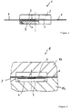
- Figure 1 Shown schematically in Figure 1 is a package having an exposed heat sink element as it appears immediately after forming the plastic case.
- the package is shown in a side view taken parallel to the direction of the leads, and partly in section in the left-hand portion of the figure. The cross-section is the obliquely hatched area.
- the package is generally denoted by 1 in that figure.
- That figure and the following ones illustrate by way of example a package of the DIP (Dual-In line Package) type, that is one having its leads projecting out from two opposite sides of the package body.
- DIP Dual-In line Package
- the semiconductor material die has been omitted from the sectional view.
- a plastic case, shown at 2 has a heat sink element 3 embedded therein such that only the bottom major surface 4 thereof, at the same level as the case bottom surface, will be exposed.
- a leadframe 5 is connected to the heat sink element 3 at the opposite side from the surface 4 by connecting means such as rivets or weldings, not shown in the sectional view.
- the leadframe is partly enclosed in the case 2, so that ends of its lead, denoted by 6 extending outside, to the left and right in the figure. Shown outside the case 2, getting out of the plane determined by the case side surface in view, is a support structure 7 of the leadframe interconnecting a number of leadframes, as explained hereinafter.
- Each heat sink element is obtained by shearing from a relatively thick sheet of metal, e.g. copper. From a thinner sheet, also typically of copper, a bearing structure is formed in the form of a strip and a series of leadframes, each including an assembly of narrow metal strips which are interconnected by transverse connecting lines and are intended to become the leads. To the bearing structure at each leadframe is connected a corresponding number of heat sink elements.
- a relatively thick sheet of metal e.g. copper.
- a bearing structure is formed in the form of a strip and a series of leadframes, each including an assembly of narrow metal strips which are interconnected by transverse connecting lines and are intended to become the leads.
- To the bearing structure at each leadframe is connected a corresponding number of heat sink elements.
- a corresponding number of dice are mounted integrally to this formed structure, such that each die locates at one leadframe/heat sink element structure.
- each die is connected, according to a standard technique, directly to the heat sink element without the leadframe interposed therebetween.
- the die is positioned in the central region of the heat sink element, isolated from the leads. Reference will be made in the following description to this case wherein the leadframe has no dedicated area for accommodating the die.
- the die is connected to the heat sink element either by soldering with an alloy such as tin/lead or by gluing with for example an epoxy glue.
- Another solution provides for the die being accommodated on a central portion of the corresponding leadframe, which is also connected to the heat sink element.
- Thin wires usually of gold or aluminum, are bonded with one end to dedicated metallized pads provided on the die surface where the integrated circuit is formed, and with the other end to the inward ends of the leads.
- each cavity is injected an electrically insulative material, in the molten state at a high temperature, which is to form the plastic body of the package.
- This material is typically a synthetic resin, e.g. an epoxy resin.
- Molding in the proper sense comprises the injection of the resin into the cavities. However, the molding process comprises several phases whereat the temperature is varied gradually to avoid cracking the semiconductor material that forms the die, or otherwise making the overall device unreliable.
- the term molding is used herein to denote all the operations carried out inside the mold cavity: melting the plastic material, letting it expand into the cavity and solidify.
- the plastic cases After an initial cooling step, and subsequent resin thermal curing steps to achieve thorough polymerization, the plastic cases will be completely formed, and the series of packages ready for removal from the mold.
- Figure 2 shows schematically a mold at a stage immediately preceding the molding step to form the package shown in the previous figure.
- the figure shows in particular a single mold cavity.
- a mold for the injection of resin is generally shown at 8. It comprises, in the common embodiment shown in the figure, an upper half-shell or top mold designated 8a, and a lower half-shell or bottom mold 8b. Both half molds have a corresponding hollow, and when the mold is closed, are arranged with their hollows facing each other to provide a single mold cavity whereinto the resin can be injected.
- the molten resin is injected through a gate type of inlet, designated 9 in Figure 2, formed in the mold, specifically in the bottom mold 8b, which has one end open into the mold cavity.
- the gate 9 has a substantially horizontal main axis. Its location is in any case such that the cavity can be filled even in its region at the extreme right in the figure, farthest from the resin entrance.
- the structure consisting of the heat sink element 3 and the leadframe 5 has been introduced for molding into the mold cavity, according to the configuration shown in the figure. Also shown in that figure is a die of a semiconductor material 10 fixed to the center of the top surface of the heat sink element 3 opposite from the major surface 4 to be left exposed.
- the leadframe 5 is located at the same level as the interface between the two half molds, and is positioned such that the terminating portions of the leads 6 are left outside the mold cavity.
- the mold 8 typically has one closure level only, when viewed in vertical cross-section, consisting of the surfaces at the interface of the two half molds and corresponding to the level of the leadframe 5. The presence of such a closure level is effective to make possible the introduction of the leadframe into the cavity in a easy way while allowing its outermost portions to remain outside.
- the heat sink element is located on the bottom of the mold cavity formed in the bottom mold 8b such that the bottom surface 4 will not be covered by the resin.
- the mold cavity has larger side dimensions than the heat sink element 5, and will therefore fully enclose it so as to keep the heat sink element 5 isolated laterally all around its perimeter.
- Both the bottom and top portions of the mold cavity have substantially the shape of a parallelepiped. Accordingly, the cavity shape for molding that type of package is particularly simple.
- the power package has a different structure from that shown.
- the heat sink element additionally to having a major surface exposed, will be partially extended sidewards out of the plastic case, from at least one of its sides.
- the heat sink element has two peripheral portions projecting from two opposed sides of the plastic case.
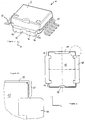
- Figure 3 is a perspective view of a known embodiment of a power package with the heat sink partially extended out of the plastic case.
- PSO package known as PSO
- the package is overall denoted by the reference numeral 11 and shown at the end of its manufacture, after bending the pins, ready to be soldered to an external electric circuit.
- the plastic case 2 partly encapsulates a heat sink element, generally denoted by 12 here, which, besides having its bottom surface exposed, extends sidewards out of the plastic case 2 in the direction denoted by y.
- a heat sink element generally denoted by 12 here, which, besides having its bottom surface exposed, extends sidewards out of the plastic case 2 in the direction denoted by y.
- the dimensions of the plastic case 2 exceed those of the corresponding sides of the heat sink element 12.
- the heat sink element 12 has in this example too peripheral portions, designated 13 in Figure 3, which symmetrically extend outwards.
- these portions 13 the top major surface 14, the side surface 15 lying in the x direction, and part of the side surfaces 16 parallel to the direction determined by the axis y are also exposed.
- the profile of the plastic case 2 and of the heat sink element 12 are determined by the particular conformation of the specific example.
- the leads, bent over to form the pins 17, are extended outside the plastic case 2 of the package 11 from opposite sides in the x direction, orthogonally to the direction along which the heat sink element 12 extends beyond the case 2.
- main cavity will be used in the following description to indicate that portion of the mold cavity which has the shape of the plastic case envelope without taking into account the presence of the heat sink element therein. Thus, it will commonly have a substantially parallelpipedic shape.
- the main mold cavity such as the mold cavity used in the example shown in Figure 2, typically results from the combination of an upper hollow formed in the top mold and a lower recess provided in the corresponding half-shell.
- the dimension of the main mold cavity along the y direction must be shorter than the length along y of the heat sink element 12.
- the mold considered overall to comprise a specific seat for the heat sink element, and in particular to provide a housing for the heat sink element which extends in the y direction outside the main mold cavity, and which is furthermore connected to the main mold cavity such that the plastic case can be formed around the heat sink element in the x direction.
- This housing is a blind hole, i.e. without side outlets, formed in the bottom portion of the mold.
- the molding technique provides for the mold to have for this purpose, additionally to a conventional first closure level corresponding to the leadframe, as in the simpler case previously discussed, a second closure level at the top major surface of the heat sink element.
- the aforementioned housing is provided at least below this level.
- Such a configuration may typically cause some drawbacks during the molding step. Specifically, problems may be encountered at the interface between the housing portions which are intended to receive the portion of the heat sink element outside the plastic case, and the main mold cavity. In fact at the second closure level, the mold sealing during the molding is specially critical. Particularly between the surfaces of the heat sink element which must be left exposed and said housing formed in the mold, the hermeticity is very difficult to achieve. Thus, during the molding step, the molten resin may partly leak out of the mold cavity in the y direction towards the most peripheral portions of the heat sink element. Over the related surfaces of the heat sink element, the leaking resin may result in the formation of flash, that is thin layers of plastic material which solidify on the external surfaces of the heat sink element.
- Figure 4 shows a schematical top view of the lower portion of a mold during the molding of the package shown in the previous figure. Both the leadframe and the semiconductor material die have been omitted, and only the heat sink element shown, for clarity reasons.
- the lower portion of the mold main cavity, denoted by 18, extends in the x direction sideways of the heat sink element 12 in connection with its central portion.
- the heat sink element 12 is disposed to have its peripheral portions 13 at the ends of a housing, denoted by 19, which is formed in the mold lower portion and extends substantially in the y direction beyond the mold main cavity 18.
- the upper closure of the housing 19 is determined by the upper structure of the mold, not shown in the figure.
- Figure 4a is an enlarged detail view of the portion enclosed within a broken line circle in Figure 4.
- a known solution to this problem provides for the use of blocking bars formed in the structure of the heat sink element at the peripheral portions thereof.
- the heat sink element/leadframe structure is formed integrally from a thick metal sheet, by shaping the heat sink element and then reducing the thickness at the sides and forming by shearing the leadframe.
- FIG. 5 A structure of this type is shown in Figure 5.
- the heavy outlined portion is the heat sink element 12, lighter lines being used to draw the leadframe 5.
- the leadframe 5 and heat sink element 12 form a mono-component and are joined to each other by blocking bars 20.
- These bars 20 of copper consist of side extensions of the peripheral portions 13 of the heat sink element 12 in the x direction. When the structure of Figure 5 is placed into the mold, the bars 20 substantially close the side channel for the resin flow indicated in Figure 4a.
- a further drawback of the known solution of Figure 5 is related to the formation of the mono-component heat sink/leadframe structure.
- the leadframe thickness cannot be less than a minimum value, if it is not to be distorted during its formation due to the weight of the heat sink element whose mass is far greater.
- Figure 6 shows schematically a vertical cross-section along the y direction through a mold made in accordance with that patent.
- Thrust elements denoted By 21, compress the heat sink element against the bottom of its housing.
- the alveolus 22 outside the heat sink element are filled with resin through suitable channels, not shown.
- Their width in the x direction is the same as that of the portions of the heat sink element which are to be left outside the plastic case.
- the plastic tips thus formed must then be removed, after taking the case out of the mold.
- This additional operation is critical especially with configurations like that shown in Figure 3 by way of example, wherein the peripheral portions of the heat sink element have the same width as the heat sink element, and substantially of the same order as the plastic case. In this instance, the plastic case may be cracked during that step.
- the underlying problem of this invention is to provide a method whereby can be formed, by only the molding process without the need of additional steps, a plastic package with an heat sink exposed and having portions extending peripherally from the plastic case kept free from resin leakouts.
- the solvent idea on which the present invention is based is founded or the consideration that it is possible to ensure, during the molding process, the hermeticity between the side surfaces of the heat sink element to be left outside the plastic case and the corresponding walls of the housing formed in the lower portion of the mold, while ensuring proper positioning of the heat sink element in its housing, by using a housing with inclined walls and by shaping the side surfaces of the heat sink element to match this inclination at least in the zone nearest the plastic case.
- a method of the type according to this invention provides for the formation of a plastic package for a power semiconductor electronic device with a partially exposed heat sink.
- the semiconductor electronic device is fully encapsulated within a plastic case and coupled thermally to a heat sink element.
- the latter has an exposed major surface and at least one peripheral portion extended outside the plastic case from at least one of its sides.
- the plastic case is formed by molding in a main cavity of a mold.
- the heat sink element has first been placed into a suitable housing provided in a lower portion of the mold, such that the major surface to be left exposed contacts the housing bottom. This housing also opens into the main cavity of the mold.
- the inclined side surfaces of the heat sink element when the mold is closed, the inclined side surfaces of the heat sink element, in its peripheral portion to be left outside the plastic case, are therefore pressed by the thrust means toward corresponding inclined walls of the housing.
- the compressive force exerted by said means and in a downward direction will have a component orthogonal to such surfaces.
- perfect temporary relative adhesion is ensured during the molding process of the side surfaces of the heat sink element to the walls of the housing in which it is located at least in the nearest zone to the mold main cavity, that is to the side of the plastic case whence the heat sink element extends. Accordingly, the hermeticity of the closure clamping of the mold is ensured even at the aforementioned second closure level by the method of this invention. In this way, bothersome leakouts of plastic material from the mold main cavity toward the peripheral portions of the heat sink element can be prevented.
- the housing for the heat sink element consists of a suitable portion of a through-going groove formed in the lower portion of the mold. According to this invention, it is indeed unnecessary to provide a blind hole for accommodating the heat sink element because the thrust elements together with the heat sink element will act as a barrier or side closure of the mold in the direction along which the heat sink element extends out of the case. The mold is, therefore, simpler to manufacture.
- each heat sink element is positioned with its central portion, to be left inside the plastic case, corresponding to widenings of the groove which will form the lower portion of the mold main cavity.
- the peripheral portion of the heat sink elements to be left outside the plastic case is properly inserted into the groove outside said widenings.
- the depths of the groove and the cavity are substantially equivalent, such that the rims of the recesses formed thereby are at the same level. In this way the lower portion of the mold can be formed by digging from the surface of the bottom mold to form both the groove and the lower portion of the cavity.
- the groove is straight and has inner side surfaces inclined through the entire groove length and has a plurality of widenings for accommodating a given number of heat sink elements positioned parallel and spaced apart from one another in the groove.
- the preferential method also provides for the heat sink elements to have inclined throughout the portion to be left outside the case those external side surfaces substantially orthogonal to the sides of the case whence they come out.
- a package for a power semiconductor electronic device comprises a plastic case to be formed by a molding process wherein at least one die of a semiconductor material is completely encapsulated which has an electronic circuit formed therein and is coupled thermally to a heat sink element having an exposed major surface and at least one peripheral portion extended out of the plastic case from at least one side thereof.
- at least side surfaces of said heat sink element extending out from said side of the plastic case form, at least in a zone adjacent to the case and in said peripheral portion, an angle substantially greater than zero with the direction of a normal line to said major surface of the heat sink element having a negative slope from outside.
- FIGS. 1 and 8 are vertical cross-section views of a mold, generally and schematically shown at 23, which embodies the principles of this invention.
- the cross-sections have been taken along directions, respectively orthogonal and parallel to the direction in which the heat sink element is extended out of the plastic case, as indicated by lines B-B and A-A, respectively, in Figure 8 and Figure 7.
- Figures 7 and 8 are parallel to the directions designated x and y, respectively.
- the figures show a single mold cavity for forming a single package, although the mold typically includes a plurality of cavities.
- the mold 23 comprises an upper half-shell or top mold 23a and a lower half-shell or bottom mold 23b. In either figures the mold is shown closed with the two half molds facing each other, as it appears typically during the molding step.
- An upper hollow and lower hollow formed in the two half molds 23a and 23b define, when the mold is closed, a mold main cavity 24 for forming the plastic case of the package.
- the two portions of the mold main cavity are marked off by an imaginary broken line between the two half molds.
- the heat sink element 25 is placed in a suitable housing, overall indicated at 26, which is formed in the lower portion of the mold 23, specifically in the bottom mold 23b.
- the bottom major surface 27 of the heat sink element is in contact with the bottom surface of the housing 26. The latter opens into the mold main cavity 24 from which it is extended outwards in the y direction, as shown in Figure 8.
- the heat sink element extends, by way of example only, out from two opposite sides of the mold main cavity and in a substantially symmetrical arrangement. However, it could be a different configuration, still remaining within the invention scope.
- the sidewalls of the housing 26 which are parallel to the y direction, that is the direction in which the heat sink element is to extended out of the plastic case, are inclined from the vertical direction, unlike conventional cases.
- these walls, indicated at 28 in the figure form an angle ⁇ with a normal direction, determined by the half lines N, to the major surfaces of the heat sink element 25, and specifically to the surface 27 or to the bottom of the housing, so as to have a positive slope from the housing interior.
- Shown at 29 in the figures are the side surfaces of the heat sink element 25 which are parallel to the y direction, to be partially enclosed within the plastic case.
- the portions of the side surfaces 29 of the heat sink element which are to be left outside the plastic case and facing said housing walls 28 are inclined, forming an angle substantially equal to ⁇ with the N direction.
- the heat sink element Prior to molding, the heat sink element must be positioned without being fixed in its housing to avoid mold wear problems and damaging the device during its removal from the mold at the end of the molding step.
- the heat sink element 25 is pushed down into the mold and caused to adhere on the inner walls in accordance with this invention during the mold closing.
- thrust means will engage from above with at least a part of the peripheral portions of the heat sink element 25 external to the mold main cavity 24 and contained within the housing 26.
- such thrust means consists of, as shown schematically in Figure 8, elements (notches) 30 jutting out of the top mold 23a and extending downwards at the side of the recess of the top mold 23a, and hence of the main mold cavity 24, and being adjacent thereto.
- the notches 30 exert a compressive force substantially downward on the peripheral portions of the heat sink element.
- the heat sink element 25, being made typically from a deformable material such as copper, undergoes a slight deformation at these portions.
- This compressive force according to this invention also applies a pressure to the side surfaces 29 of the heat sink element.
- Said force has, in fact, a non-zero component orthogonal to the latter because the direction of the force also forms an angle ⁇ with the surfaces 29.
- the latter are pressed at these portions against the corresponding inner walls 27 of the housing which are parallel to them.
- the strength of the compressive force exerted by the notches 30 is selected to cause the surfaces 29 to adhere to the walls 28.
- the barrier to the outflow of resin from the mold main cavity is provided by the combined actions of the notches down-pressing and of the heat sink element acting as a plug.
- the reliability of the resulting case is then ensured. Therefore during the package forming process no particularly complex and following steps of removing residual resin are needed. The process is, therefore, particularly simple, and the overall device packaging time is advantageously shortened.
- the angle ⁇ is selected illustratively to avoid difficulties in manufacturing the mold and heat sink element; it may be selected to be typically smaller than 30°.
- the housing 26 can be advantageously utilized as a guide in positioning the heat sink element 25 inside it. This can be seen as a self-aligning feature in the x direction since the heat sink element 25, if placed twisted by mistake, would automatically turn and regain its correct position. Due to this problem, prior processes required manual intervention or at least additional checking of the heat sink element for placing it in a proper position.
- the invention allows automatic machines of the pick-and-place type to be used which would pick and position heat sink elements without any further checking.
- the housing for the heat sink element need not be delimited in the y direction; this because of the apparatus configuration ensuring perfect closing of the mold cavities even in this direction.
- the two horizontal broken lines indicated at 32, at the level of the bottom surface 27 of the heat sink element 25, denote that the housing structure may be extended beyond the length of the heat sink element in the y direction along which it extends cut of the mold main cavity.
- a method for forming a PSO type of package such as that illustrated in connection with the prior art of Figure 3.
- the package is of the dual-in-line type, with electric interconnecting pins coming out of the package from two opposed sides and orthogonally to the direction in which the heat sink element is extended out of the plastic case.
- Figure 9 shows a perspective view of a mold open at the end of the molding operation for the plastic case of the package.
- the mold is shown referring to a single device.
- Figure 10 shows a vertical cross-section taken in the orthogonal direction to that of outward extension of the heat sink element, namely the y direction of Figure 9.
- the mold is overall shown at 33, and in both figures only its lower portion 33b is in view.
- the plastic case 2 is partially inserted into the lower portion of the mold main cavity and projects upwardly from the bottom mold 33b.
- a groove 34 is provided in the bottom mold 33b which goes through the bottom mold 33b from one side to other.
- the groove 34 has a main axis along the direction in which the heat sink element 25 is to extend out of the plastic case 2, i.e. parallel to the y direction.
- the width of the groove 34 is equal to the dimension along x of the heat sink element 25.
- the walls of the groove 34 parallel to the y direction, indicated at 28' in these figures, are inclined, according to this invention, at an angle ⁇ from the normal N.
- an angle ⁇ around the 15° range was selected.
- the depth of the groove 34 is such that its bottom locates correspondingly to the bottom surface of the package. Its edge is at the level of the leadframe, that is of the separation line between the two half molds, so that the leads can be left outside the mold cavity. Essentially, its depth is the same as that of the lower main mold cavity.
- the lower portion of the mold main cavity forms a enlargement in the x direction of the groove 34 at the location where the heat sink element 25 is to be placed.
- the heat sink element is disposed such that its central portion, to be encapsulated within the plastic case, is in correspondence with said enlargement, and with its peripheral portions within the groove 34 but outside the enlargement.
- the side surfaces 28' of the heat sink element are correspondingly inclined at least inside the groove in the portions outside the plastic case, and in contact with the groove walls.
- the central portions of the side surfaces of the heat sink element are similarly arranged, since they are engaged in the groove, without contacting any walls, being faced the enlargement formed by the lower mold cavity.
- these central portions are not inclined but are orthogonal to the bottom major surface 27 of the heat sink element.
- peripheral surfaces of the plastic case, and correspondingly therewith the inner walls, not visible, of the mold cavity, are inclined as in the conventional structure for easy removal from the mold, independently of the objects of this invention.
- the through-going groove can accommodate a given number of heat sink elements, typically some tens of them, placed parallel.
- the groove 34 could contain about fifteen heat sink elements, and the bottom mold 33b was formed with several parallel through-going trenches.
- each groove 34 is formed from one side to another into a main surface of the bottom mold. It has the appearance of a hollow with inclined walls, having a single main axis and presenting a corresponding number of widenings, also parallel to one another and spaced apart at the locations where the heat sink elements 25 will be placed.
- the heat sink elements are typically placed into the groove simultaneously, after riveting them to a single metal strip which includes their respective lead frames.
- the heat sink elements could be placed into the groove sequentially, for a different process wherein the heat sinks are attached to the leadframes after being placed into the mold.
- the heat sink element 25 can be placed into the mold 33b in a particularly easy manner, in this preferential embodiment wherein the housing for the heat sink element is other than a blind hole.
- the groove represents a straight guide having possible the placement of each heat sink element may be laid in place by inserting it laterally of the mold through one of the two side months of the groove.
- the notches are formed on the upper portion, not shown in the figures, of the groove, and fit into the groove 34 upon closing the mold, to engage the portions of the heat sink element which lie outside the main cavity. It is on this account that the notches are formed laterally of the upper portion of the mold main cavity. Their width is substantially the same as that of the groove. For each mold cavity, a pair of notches are typically provided on opposing sides such that, between adjacent cavities, there will be two limited notches in the y direction. In an alternative embodiment, two notches of two adjacent cavities may be joined into a single, extended notch between the two adjacent cavities, adapted to be inserted inside the groove. Their height is such that their tips, with the mold closed, will not reach the bottom, but stop at the same level as the upper major surface of the underlying heat sink element.
- the mold structure and in particular that of its lower portion, is therefore particularly simple according to the preferential embodiment of this invention.
- this affords lower manufacturing costs than conventional molds.
- the mold needed to have a more complicated structure. Nowhere could an "open" configuration like that of our preferential embodiment with a through-going groove be used, since it was necessary to define a delimited area in the bottom mold for containing the plastic material.
- Figure 11 shows the package, overall indicated at 35, after its removal from the mold 33 and subsequent steps wherein the individual packages are separated from one another (the singulation step) by cutting the metal strip on which the series of lead frames are formed, and the leads are bent to form the pins 17.
- the heat sink element 25 has, in the peripheral portions 36 outside the plastic case 2, as shown in the figure, its side surfaces 29, parallel to the y direction, inclined from an orthogonal straight line to the major surfaces of the heat sink element with a negative outward slope.
- the portions of such surfaces inside the plastic case, not in view in Figure 11, are instead orthogonal to the major surfaces of the heat sink element 25.
- these central portions have a different, slightly smaller width than the outwardly extended portion.
- this invention has been particularly illustrated in connection with packages of the dual-in-line type, this invention may also be applied to packages having projecting pins from one side only of the plastic case, that is of the single-in-line type.
- the pins could project for equal effect either orthogonal or parallel to the direction in which the plastic case is extended outwardly, both in the dual-in-line version illustrated herein and the single-in-line version.
- the through-going groove illustrated in the preferential embodiment could be non-straight and follow a different pattern, but always including corresponding to each heat sink element portions adapted to accommodate, for example, a single heat sink element. These portions may typically have a main axial direction parallel to the direction along which the heat sink element extends outwards from the plastic case.
- the through-going groove may have the overall pattern of a polygonal line.
- each through-going groove may vary to suit particular applications. In the extreme, each through-going groove could accommodate only one heat sink element.
- the depth of the groove described by the figures is greater than the height of the heat sink element it is to receive, but its functionality would not change even if a particular applications required a groove of smaller or equal depth, with the heat sink element extending upwardly toward the upper portion of the mold main cavity.
- the side surfaces of the heat sink element lying parallel to the y direction could be, in a different embodiment, inclined also at their central portion embedded within the plastic case, in a simplified, easily manufactured construction. In the extreme, the side surfaces parallel to the x direction and completely outside the plastic case could also be inclined, and still fall within the scope of the present invention.
- the heat sink element should extend out of the case in a symmetrical way is no strict requirement, nor is that it should be symmetrical.
- the heat sink element may have different shapes and dimensions also in the respect of the plastic case, and its width along x could be the same as that of the case, for example.
- the figures described relate to the typical instance of the beat sink element being extended outside the plastic case from two opposite sides.
- the heat sink element could come out from one side only, so being anyway determined a y direction along which the walls of its housing would be inclined.
- side surfaces of the heat sink element could jut out of the plastic case in a direction different than a direction orthogonal to the respective side of the case.
- the housing would no longer have a single main direction, but in accordance with this invention its walls would have to be inclined at least in each portion in contact with side surfaces, also correspondingly inclined, of the heat sink element, near and outside the plastic case.
Priority Applications (4)
| Application Number | Priority Date | Filing Date | Title |
|---|---|---|---|
| DE69636853T DE69636853T2 (de) | 1996-11-27 | 1996-11-27 | Herstellunsgverfahren einer Kunststoffpackung für elektronische Anordnungen mit einer Wärmesenke |
| EP96830597A EP0845801B1 (fr) | 1996-11-27 | 1996-11-27 | Procédé de fabrication d'un empaquetage en plastique pour des dispositifs électroniques ayant un dissipateur de chaleur |
| US08/978,548 US5953593A (en) | 1996-11-27 | 1997-11-26 | Method and mold for manufacturing a plastic package for an electronic device having a heat sink |
| JP9325953A JPH10256291A (ja) | 1996-11-27 | 1997-11-27 | 熱散逸器を具備する電子装置用プラスチックパッケージの製造方法 |
Applications Claiming Priority (1)
| Application Number | Priority Date | Filing Date | Title |
|---|---|---|---|
| EP96830597A EP0845801B1 (fr) | 1996-11-27 | 1996-11-27 | Procédé de fabrication d'un empaquetage en plastique pour des dispositifs électroniques ayant un dissipateur de chaleur |
Publications (2)
| Publication Number | Publication Date |
|---|---|
| EP0845801A1 true EP0845801A1 (fr) | 1998-06-03 |
| EP0845801B1 EP0845801B1 (fr) | 2007-01-17 |
Family
ID=8226062
Family Applications (1)
| Application Number | Title | Priority Date | Filing Date |
|---|---|---|---|
| EP96830597A Expired - Lifetime EP0845801B1 (fr) | 1996-11-27 | 1996-11-27 | Procédé de fabrication d'un empaquetage en plastique pour des dispositifs électroniques ayant un dissipateur de chaleur |
Country Status (4)
| Country | Link |
|---|---|
| US (1) | US5953593A (fr) |
| EP (1) | EP0845801B1 (fr) |
| JP (1) | JPH10256291A (fr) |
| DE (1) | DE69636853T2 (fr) |
Families Citing this family (8)
| Publication number | Priority date | Publication date | Assignee | Title |
|---|---|---|---|---|
| US20080258282A1 (en) * | 2007-04-23 | 2008-10-23 | Hua Yang | Lead frame free package and method of making |
| CN101765741B (zh) * | 2007-05-25 | 2012-07-04 | 莫列斯公司 | 用于发热装置与电源的散热器 |
| JP5233973B2 (ja) * | 2009-12-01 | 2013-07-10 | 株式会社デンソー | モールドパッケージの製造方法 |
| JP2011201237A (ja) * | 2010-03-26 | 2011-10-13 | Yamatake Corp | 筐体組立構造及び筐体組立方法 |
| JP5903785B2 (ja) * | 2011-07-19 | 2016-04-13 | トヨタ自動車株式会社 | 半導体装置製造方法 |
| JP2016076734A (ja) * | 2016-01-28 | 2016-05-12 | トヨタ自動車株式会社 | 半導体装置 |
| KR102420700B1 (ko) | 2017-09-28 | 2022-07-13 | 미쓰비시덴키 가부시키가이샤 | 반도체 장치, 고주파 전력 증폭기, 및, 반도체 장치의 제조 방법 |
| CN114347341B (zh) * | 2021-12-31 | 2024-04-09 | 佛山市国星光电股份有限公司 | 一种分立器件塑封装置及塑封方法 |
Citations (6)
| Publication number | Priority date | Publication date | Assignee | Title |
|---|---|---|---|---|
| DE1944098A1 (de) * | 1968-09-02 | 1970-03-12 | Sanyo Electric Co | Halbleiteranordnung |
| JPH04116942A (ja) * | 1990-09-07 | 1992-04-17 | Nec Corp | 樹脂封止型半導体装置の製造方法及び封止用金型 |
| EP0539095A2 (fr) * | 1991-10-23 | 1993-04-28 | Fujitsu Limited | Dispositif semi-conducteur comprenant une structure de radiateur et procédé de fabrication associé |
| EP0545007A1 (fr) | 1991-11-29 | 1993-06-09 | STMicroelectronics S.r.l. | Structure pour dispositif semi-conducteur comprenant un dissipateur de chaleur et un corps en plastique, et moyens extrêmement fiables pour sa connexion électrique au dissipateur de chaleur |
| JPH0661400A (ja) * | 1992-08-10 | 1994-03-04 | Fujitsu Ltd | ヒートシンク付樹脂パッケージ半導体装置の製造方法 |
| US5445995A (en) * | 1991-12-20 | 1995-08-29 | Sgs-Thomson Microelectronics, S.R.L. | Method for manufacturing plastic-encapsulated semiconductor devices with exposed metal heat sink |
-
1996
- 1996-11-27 EP EP96830597A patent/EP0845801B1/fr not_active Expired - Lifetime
- 1996-11-27 DE DE69636853T patent/DE69636853T2/de not_active Expired - Lifetime
-
1997
- 1997-11-26 US US08/978,548 patent/US5953593A/en not_active Expired - Lifetime
- 1997-11-27 JP JP9325953A patent/JPH10256291A/ja active Pending
Patent Citations (6)
| Publication number | Priority date | Publication date | Assignee | Title |
|---|---|---|---|---|
| DE1944098A1 (de) * | 1968-09-02 | 1970-03-12 | Sanyo Electric Co | Halbleiteranordnung |
| JPH04116942A (ja) * | 1990-09-07 | 1992-04-17 | Nec Corp | 樹脂封止型半導体装置の製造方法及び封止用金型 |
| EP0539095A2 (fr) * | 1991-10-23 | 1993-04-28 | Fujitsu Limited | Dispositif semi-conducteur comprenant une structure de radiateur et procédé de fabrication associé |
| EP0545007A1 (fr) | 1991-11-29 | 1993-06-09 | STMicroelectronics S.r.l. | Structure pour dispositif semi-conducteur comprenant un dissipateur de chaleur et un corps en plastique, et moyens extrêmement fiables pour sa connexion électrique au dissipateur de chaleur |
| US5445995A (en) * | 1991-12-20 | 1995-08-29 | Sgs-Thomson Microelectronics, S.R.L. | Method for manufacturing plastic-encapsulated semiconductor devices with exposed metal heat sink |
| JPH0661400A (ja) * | 1992-08-10 | 1994-03-04 | Fujitsu Ltd | ヒートシンク付樹脂パッケージ半導体装置の製造方法 |
Non-Patent Citations (3)
| Title |
|---|
| EHNERT A ET AL: "A NEW SURFACE MOUNT POWER PACKAGE", 7 March 1993, PROCEEDINGS OF THE ANNUAL APPLIED POWER ELECTRONICS CONFERENCE AND EXPOSITION (APEC), SAN DIEGO, MAR. 7 - 11, 1993, NR. CONF. 8, PAGE(S) 380 - 384, INSTITUTE OF ELECTRICAL AND ELECTRONICS ENGINEERS, XP000357919 * |
| PATENT ABSTRACTS OF JAPAN vol. 016, no. 367 (E - 1245) 7 August 1992 (1992-08-07) * |
| PATENT ABSTRACTS OF JAPAN vol. 018, no. 299 (E - 1558) 8 June 1994 (1994-06-08) * |
Also Published As
| Publication number | Publication date |
|---|---|
| JPH10256291A (ja) | 1998-09-25 |
| DE69636853D1 (de) | 2007-03-08 |
| US5953593A (en) | 1999-09-14 |
| DE69636853T2 (de) | 2007-11-08 |
| EP0845801B1 (fr) | 2007-01-17 |
Similar Documents
| Publication | Publication Date | Title |
|---|---|---|
| US5625536A (en) | Semiconductor device | |
| US5904506A (en) | Semiconductor device suitable for testing | |
| US6262480B1 (en) | Package for electronic device having a fully insulated dissipator | |
| US5278446A (en) | Reduced stress plastic package | |
| US7541669B2 (en) | Semiconductor device package with base features to reduce leakage | |
| KR100238601B1 (ko) | 전자장치 | |
| US6627976B1 (en) | Leadframe for semiconductor package and mold for molding the same | |
| US6114189A (en) | Molded array integrated circuit package | |
| KR20080027920A (ko) | 반도체 디바이스 | |
| JP2002033438A (ja) | 樹脂封入型回路装置 | |
| KR101017533B1 (ko) | 오버몰드된 플라스틱 패키지를 위한 히트싱크 또는플래그용 소형 몰드로크들 | |
| US4503452A (en) | Plastic encapsulated semiconductor device and method for manufacturing the same | |
| US5244838A (en) | Process and apparatus for assembling and resin-encapsulating a heat sink-mounted semiconductor power device | |
| EP0069390B1 (fr) | Cadre de connexion pour dispositif semiconducteur encapsulé en plastique | |
| US8466009B2 (en) | Method of fabricating a semiconductor package with mold lock opening | |
| EP0845801B1 (fr) | Procédé de fabrication d'un empaquetage en plastique pour des dispositifs électroniques ayant un dissipateur de chaleur | |
| WO1992002953A1 (fr) | Boitier de circuit integre moule | |
| US5225897A (en) | Molded package for semiconductor devices with leadframe locking structure | |
| EP0807973B1 (fr) | Dispositif semi-conducteur du type à incapsulation en plastique et procédé de fabrication | |
| EP1318544A1 (fr) | Procédé de fabrication de dispositifs à semi-conducteur en boítier | |
| JPH088375A (ja) | 半導体装置およびその製造に使用されるリードフレーム並びに金型 | |
| JP7435417B2 (ja) | 半導体装置用インサートケースの製造方法及び半導体装置 | |
| KR970010671B1 (ko) | 집적회로장치용 히트싱크를 구비한 플라스틱 몰드 패키지 | |
| JP2802966B2 (ja) | 樹脂封止型電子部品の製造方法 | |
| CN116779549A (zh) | 半导体封装结构及半导体封装器件 |
Legal Events
| Date | Code | Title | Description |
|---|---|---|---|
| PUAI | Public reference made under article 153(3) epc to a published international application that has entered the european phase |
Free format text: ORIGINAL CODE: 0009012 |
|
| AK | Designated contracting states |
Kind code of ref document: A1 Designated state(s): DE FR GB IT |
|
| AX | Request for extension of the european patent |
Free format text: AL;LT;LV;RO;SI |
|
| RAP3 | Party data changed (applicant data changed or rights of an application transferred) |
Owner name: STMICROELECTRONICS S.R.L. |
|
| 17P | Request for examination filed |
Effective date: 19981123 |
|
| AKX | Designation fees paid |
Free format text: DE FR GB IT |
|
| RBV | Designated contracting states (corrected) |
Designated state(s): DE FR GB IT |
|
| 17Q | First examination report despatched |
Effective date: 20030902 |
|
| RIC1 | Information provided on ipc code assigned before grant |
Ipc: 7H 01L 23/433 B Ipc: 7H 01L 21/56 A |
|
| GRAP | Despatch of communication of intention to grant a patent |
Free format text: ORIGINAL CODE: EPIDOSNIGR1 |
|
| GRAS | Grant fee paid |
Free format text: ORIGINAL CODE: EPIDOSNIGR3 |
|
| GRAA | (expected) grant |
Free format text: ORIGINAL CODE: 0009210 |
|
| AK | Designated contracting states |
Kind code of ref document: B1 Designated state(s): DE FR GB IT |
|
| REG | Reference to a national code |
Ref country code: GB Ref legal event code: FG4D |
|
| REF | Corresponds to: |
Ref document number: 69636853 Country of ref document: DE Date of ref document: 20070308 Kind code of ref document: P |
|
| ET | Fr: translation filed | ||
| PLBE | No opposition filed within time limit |
Free format text: ORIGINAL CODE: 0009261 |
|
| STAA | Information on the status of an ep patent application or granted ep patent |
Free format text: STATUS: NO OPPOSITION FILED WITHIN TIME LIMIT |
|
| 26N | No opposition filed |
Effective date: 20071018 |
|
| PG25 | Lapsed in a contracting state [announced via postgrant information from national office to epo] |
Ref country code: IT Free format text: LAPSE BECAUSE OF FAILURE TO SUBMIT A TRANSLATION OF THE DESCRIPTION OR TO PAY THE FEE WITHIN THE PRESCRIBED TIME-LIMIT Effective date: 20070117 |
|
| GBPC | Gb: european patent ceased through non-payment of renewal fee |
Effective date: 20071127 |
|
| PG25 | Lapsed in a contracting state [announced via postgrant information from national office to epo] |
Ref country code: GB Free format text: LAPSE BECAUSE OF NON-PAYMENT OF DUE FEES Effective date: 20071127 |
|
| PGFP | Annual fee paid to national office [announced via postgrant information from national office to epo] |
Ref country code: DE Payment date: 20131022 Year of fee payment: 18 Ref country code: FR Payment date: 20131121 Year of fee payment: 18 |
|
| REG | Reference to a national code |
Ref country code: DE Ref legal event code: R119 Ref document number: 69636853 Country of ref document: DE |
|
| REG | Reference to a national code |
Ref country code: FR Ref legal event code: ST Effective date: 20150731 |
|
| PG25 | Lapsed in a contracting state [announced via postgrant information from national office to epo] |
Ref country code: DE Free format text: LAPSE BECAUSE OF NON-PAYMENT OF DUE FEES Effective date: 20150602 |
|
| PG25 | Lapsed in a contracting state [announced via postgrant information from national office to epo] |
Ref country code: FR Free format text: LAPSE BECAUSE OF NON-PAYMENT OF DUE FEES Effective date: 20141201 |