EP0838698A2 - Lichttransparentes, Wärmestrahlung reflektierendes Schichtensystem - Google Patents
Lichttransparentes, Wärmestrahlung reflektierendes Schichtensystem Download PDFInfo
- Publication number
- EP0838698A2 EP0838698A2 EP97112249A EP97112249A EP0838698A2 EP 0838698 A2 EP0838698 A2 EP 0838698A2 EP 97112249 A EP97112249 A EP 97112249A EP 97112249 A EP97112249 A EP 97112249A EP 0838698 A2 EP0838698 A2 EP 0838698A2
- Authority
- EP
- European Patent Office
- Prior art keywords
- layer
- layer system
- carbon
- diamond
- layers
- Prior art date
- Legal status (The legal status is an assumption and is not a legal conclusion. Google has not performed a legal analysis and makes no representation as to the accuracy of the status listed.)
- Ceased
Links
- 229910003460 diamond Inorganic materials 0.000 claims abstract description 35
- 239000010432 diamond Substances 0.000 claims abstract description 35
- 239000000758 substrate Substances 0.000 claims abstract description 20
- OKTJSMMVPCPJKN-UHFFFAOYSA-N Carbon Chemical compound [C] OKTJSMMVPCPJKN-UHFFFAOYSA-N 0.000 claims abstract description 16
- 229910052799 carbon Inorganic materials 0.000 claims abstract description 16
- 230000005855 radiation Effects 0.000 claims abstract description 12
- 230000003595 spectral effect Effects 0.000 claims abstract description 12
- 230000005540 biological transmission Effects 0.000 claims abstract description 3
- 230000003287 optical effect Effects 0.000 claims description 6
- XLOMVQKBTHCTTD-UHFFFAOYSA-N Zinc monoxide Chemical compound [Zn]=O XLOMVQKBTHCTTD-UHFFFAOYSA-N 0.000 claims description 5
- 230000006978 adaptation Effects 0.000 claims description 5
- 238000000034 method Methods 0.000 claims description 5
- VYPSYNLAJGMNEJ-UHFFFAOYSA-N Silicium dioxide Chemical compound O=[Si]=O VYPSYNLAJGMNEJ-UHFFFAOYSA-N 0.000 claims description 4
- GWEVSGVZZGPLCZ-UHFFFAOYSA-N Titan oxide Chemical compound O=[Ti]=O GWEVSGVZZGPLCZ-UHFFFAOYSA-N 0.000 claims description 4
- 239000011521 glass Substances 0.000 claims description 4
- 239000000463 material Substances 0.000 claims description 4
- XOLBLPGZBRYERU-UHFFFAOYSA-N tin dioxide Chemical compound O=[Sn]=O XOLBLPGZBRYERU-UHFFFAOYSA-N 0.000 claims description 3
- 229910001887 tin oxide Inorganic materials 0.000 claims description 3
- 239000011787 zinc oxide Substances 0.000 claims description 3
- 229910052582 BN Inorganic materials 0.000 claims description 2
- ZOXJGFHDIHLPTG-UHFFFAOYSA-N Boron Chemical compound [B] ZOXJGFHDIHLPTG-UHFFFAOYSA-N 0.000 claims description 2
- PZNSFCLAULLKQX-UHFFFAOYSA-N Boron nitride Chemical compound N#B PZNSFCLAULLKQX-UHFFFAOYSA-N 0.000 claims description 2
- 229910052796 boron Inorganic materials 0.000 claims description 2
- 238000005234 chemical deposition Methods 0.000 claims description 2
- 238000005229 chemical vapour deposition Methods 0.000 claims description 2
- 239000012535 impurity Substances 0.000 claims description 2
- 238000004519 manufacturing process Methods 0.000 claims description 2
- TWNQGVIAIRXVLR-UHFFFAOYSA-N oxo(oxoalumanyloxy)alumane Chemical compound O=[Al]O[Al]=O TWNQGVIAIRXVLR-UHFFFAOYSA-N 0.000 claims description 2
- 235000012239 silicon dioxide Nutrition 0.000 claims description 2
- 239000000377 silicon dioxide Substances 0.000 claims description 2
- 239000004408 titanium dioxide Substances 0.000 claims description 2
- 150000001875 compounds Chemical class 0.000 claims 1
- 239000010410 layer Substances 0.000 description 111
- 229910052751 metal Inorganic materials 0.000 description 6
- 239000002184 metal Substances 0.000 description 6
- 229910044991 metal oxide Inorganic materials 0.000 description 6
- 230000007613 environmental effect Effects 0.000 description 5
- 150000004706 metal oxides Chemical class 0.000 description 5
- 239000000126 substance Substances 0.000 description 5
- 239000005357 flat glass Substances 0.000 description 3
- 239000011241 protective layer Substances 0.000 description 3
- -1 Compounds zinc oxide Chemical class 0.000 description 2
- BQCADISMDOOEFD-UHFFFAOYSA-N Silver Chemical compound [Ag] BQCADISMDOOEFD-UHFFFAOYSA-N 0.000 description 2
- 239000005328 architectural glass Substances 0.000 description 2
- 238000005137 deposition process Methods 0.000 description 2
- 150000002739 metals Chemical class 0.000 description 2
- 229910052709 silver Inorganic materials 0.000 description 2
- 239000004332 silver Substances 0.000 description 2
- 229910018072 Al 2 O 3 Inorganic materials 0.000 description 1
- RYGMFSIKBFXOCR-UHFFFAOYSA-N Copper Chemical compound [Cu] RYGMFSIKBFXOCR-UHFFFAOYSA-N 0.000 description 1
- YZCKVEUIGOORGS-UHFFFAOYSA-N Hydrogen atom Chemical compound [H] YZCKVEUIGOORGS-UHFFFAOYSA-N 0.000 description 1
- 229910004298 SiO 2 Inorganic materials 0.000 description 1
- 229910006404 SnO 2 Inorganic materials 0.000 description 1
- 229910010413 TiO 2 Inorganic materials 0.000 description 1
- 238000005299 abrasion Methods 0.000 description 1
- 229910045601 alloy Inorganic materials 0.000 description 1
- 239000000956 alloy Substances 0.000 description 1
- 230000003667 anti-reflective effect Effects 0.000 description 1
- 239000012876 carrier material Substances 0.000 description 1
- 238000004140 cleaning Methods 0.000 description 1
- 229910052802 copper Inorganic materials 0.000 description 1
- 239000010949 copper Substances 0.000 description 1
- 230000005672 electromagnetic field Effects 0.000 description 1
- 239000007789 gas Substances 0.000 description 1
- PCHJSUWPFVWCPO-UHFFFAOYSA-N gold Chemical compound [Au] PCHJSUWPFVWCPO-UHFFFAOYSA-N 0.000 description 1
- 229910052737 gold Inorganic materials 0.000 description 1
- 239000010931 gold Substances 0.000 description 1
- 229910052738 indium Inorganic materials 0.000 description 1
- APFVFJFRJDLVQX-UHFFFAOYSA-N indium atom Chemical compound [In] APFVFJFRJDLVQX-UHFFFAOYSA-N 0.000 description 1
- AMGQUBHHOARCQH-UHFFFAOYSA-N indium;oxotin Chemical compound [In].[Sn]=O AMGQUBHHOARCQH-UHFFFAOYSA-N 0.000 description 1
- 238000009776 industrial production Methods 0.000 description 1
- 239000002346 layers by function Substances 0.000 description 1
- 239000002245 particle Substances 0.000 description 1
- OANVFVBYPNXRLD-UHFFFAOYSA-M propyromazine bromide Chemical compound [Br-].C12=CC=CC=C2SC2=CC=CC=C2N1C(=O)C(C)[N+]1(C)CCCC1 OANVFVBYPNXRLD-UHFFFAOYSA-M 0.000 description 1
- 230000000284 resting effect Effects 0.000 description 1
- 230000000007 visual effect Effects 0.000 description 1
Images
Classifications
-
- G—PHYSICS
- G02—OPTICS
- G02B—OPTICAL ELEMENTS, SYSTEMS OR APPARATUS
- G02B5/00—Optical elements other than lenses
- G02B5/20—Filters
- G02B5/208—Filters for use with infrared or ultraviolet radiation, e.g. for separating visible light from infrared and/or ultraviolet radiation
-
- B—PERFORMING OPERATIONS; TRANSPORTING
- B32—LAYERED PRODUCTS
- B32B—LAYERED PRODUCTS, i.e. PRODUCTS BUILT-UP OF STRATA OF FLAT OR NON-FLAT, e.g. CELLULAR OR HONEYCOMB, FORM
- B32B7/00—Layered products characterised by the relation between layers; Layered products characterised by the relative orientation of features between layers, or by the relative values of a measurable parameter between layers, i.e. products comprising layers having different physical, chemical or physicochemical properties; Layered products characterised by the interconnection of layers
- B32B7/02—Physical, chemical or physicochemical properties
- B32B7/023—Optical properties
-
- B—PERFORMING OPERATIONS; TRANSPORTING
- B32—LAYERED PRODUCTS
- B32B—LAYERED PRODUCTS, i.e. PRODUCTS BUILT-UP OF STRATA OF FLAT OR NON-FLAT, e.g. CELLULAR OR HONEYCOMB, FORM
- B32B9/00—Layered products comprising a layer of a particular substance not covered by groups B32B11/00 - B32B29/00
- B32B9/005—Layered products comprising a layer of a particular substance not covered by groups B32B11/00 - B32B29/00 comprising one layer of ceramic material, e.g. porcelain, ceramic tile
- B32B9/007—Layered products comprising a layer of a particular substance not covered by groups B32B11/00 - B32B29/00 comprising one layer of ceramic material, e.g. porcelain, ceramic tile comprising carbon, e.g. graphite, composite carbon
-
- Y—GENERAL TAGGING OF NEW TECHNOLOGICAL DEVELOPMENTS; GENERAL TAGGING OF CROSS-SECTIONAL TECHNOLOGIES SPANNING OVER SEVERAL SECTIONS OF THE IPC; TECHNICAL SUBJECTS COVERED BY FORMER USPC CROSS-REFERENCE ART COLLECTIONS [XRACs] AND DIGESTS
- Y10—TECHNICAL SUBJECTS COVERED BY FORMER USPC
- Y10T—TECHNICAL SUBJECTS COVERED BY FORMER US CLASSIFICATION
- Y10T428/00—Stock material or miscellaneous articles
- Y10T428/24—Structurally defined web or sheet [e.g., overall dimension, etc.]
- Y10T428/24942—Structurally defined web or sheet [e.g., overall dimension, etc.] including components having same physical characteristic in differing degree
- Y10T428/2495—Thickness [relative or absolute]
- Y10T428/24967—Absolute thicknesses specified
- Y10T428/24975—No layer or component greater than 5 mils thick
-
- Y—GENERAL TAGGING OF NEW TECHNOLOGICAL DEVELOPMENTS; GENERAL TAGGING OF CROSS-SECTIONAL TECHNOLOGIES SPANNING OVER SEVERAL SECTIONS OF THE IPC; TECHNICAL SUBJECTS COVERED BY FORMER USPC CROSS-REFERENCE ART COLLECTIONS [XRACs] AND DIGESTS
- Y10—TECHNICAL SUBJECTS COVERED BY FORMER USPC
- Y10T—TECHNICAL SUBJECTS COVERED BY FORMER US CLASSIFICATION
- Y10T428/00—Stock material or miscellaneous articles
- Y10T428/30—Self-sustaining carbon mass or layer with impregnant or other layer
Definitions
- Such a low-E layer system is, for example described in DE 42 11 363.
- the real one Functional layer represents the metal layer are made of metals with very low radiation emission coefficients consists.
- the metal layer consists of silver, gold or also from copper or alloys of these metals.
- the metal oxide layers serve the purpose as an anti-reflective layer to act and at the same time the metal layer against mechanical and / or chemical Protect environmental impacts.
- multi-layer protective layers that determine the resistance behavior generic in relation to environmental influences Increase low-E layer systems.
- ITO indium tin oxide
- tin oxide used, e.g. for cost reasons pyrolytically applied to the carrier material and have an emissivity value of 0.4.
- the invention is based on the object Low-E layer system of the type mentioned at the beginning to create which has increased durability against chemical and / or mechanical influences has and the shortcomings of the known technical Avoids solutions.
- this object is achieved by a low-E layer system which has at least one carbon layer doped with foreign atoms and crystallized out in a diamond structure, the radiation emissivity in the heat radiation spectral range and the electrical conductivity of this diamond layer being adjustable as a function of the doping concentration c A of the foreign atoms in the carbon layer .
- Boron doping is proposed as doping material according to claim 2, whereby the diamond layer has p-type conduction.
- doped diamond layers according to the invention for low-E layer systems has the decisive advantage that layers of this type have low emissivity in the infrared spectral range on the one hand, high transparency in the visual spectral range and also the physical and chemical properties desired for such layer systems, namely a great hardness, high abrasion resistance and thus a chemical resistance to any environmental influences.
- the invention particularly advantageously provides a layer system which has comparatively low emissivity values as conventional, silver-based low-E layer systems, but avoids their low resistance to environmental influences.
- Low-E layer systems according to the invention can thus be used advantageously, for example, on the outer surfaces of glass windows.
- the inventive doped diamond layer between two high-purity to embed undoped diamond layers, so that the low-e layer system as a whole three arranged one on top of the other on a substrate Layers.
- the individual diamond layers having individual layers to produce synthetically.
- a plasma chemical deposition process preferably a chemical vapor deposition process, i.e. CVD, proposed.
- CVD chemical vapor deposition process
- Diamond layers from the gas phase with the addition of atomic hydrogen deposited on a substrate This method can be used on substrates closed, polycrystalline to be deposited Synthesize diamond layers that according to the invention can be used as low-E layers.
- the layers 14 and 18 each consist of high-purity, preferably polycrystalline, in diamond structure crystallized carbon layers.
- the layers 14, 16, 18 are each by means of a CVD deposition process deposited on the substrate 2.
- the substrate 2 consists of a light-transparent Vitreous, e.g. a window glass.
- the low-E layer systems shown in FIG. 1 or FIG. 2 are e.g. as an electrically conductive Layer system for use with automotive windows usable, the conductive layers by means of Current flow can be heated as an ohmic resistor are and for deicing the car windows to serve. Furthermore, the layer systems shown are shielding as electromagnetic fields, light-transparent wall can be used.
- the low-E layer systems shown in FIGS. 1 and 2 15 and 3 are on the order Exterior surfaces of architectural glass provided, which e.g. in climates with abrasive on glass surfaces acting particles, e.g. Sand Wind currents to be used or which through intensive cleaning processes high chemical and / or exposed to physical loads are.
- architectural glass e.g. in climates with abrasive on glass surfaces acting particles, e.g. Sand Wind currents to be used or which through intensive cleaning processes high chemical and / or exposed to physical loads are.
Landscapes
- Physics & Mathematics (AREA)
- Health & Medical Sciences (AREA)
- Toxicology (AREA)
- General Physics & Mathematics (AREA)
- Optics & Photonics (AREA)
- Chemical & Material Sciences (AREA)
- Engineering & Computer Science (AREA)
- Ceramic Engineering (AREA)
- Surface Treatment Of Glass (AREA)
- Laminated Bodies (AREA)
- Optical Filters (AREA)
Abstract
Description
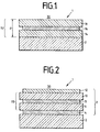
Substrat / Metalloxyd / Metall / Metalloxyd.
- Figur 1
- ein drei Einzelschichten umfassendes Low-E-Schichtensystem, aufgebracht auf einem Substrat;
- Figur 2
- ein aus fünf Einzelschichten bestehendes Low-E-Schichtensystem auf einem Substrat.
- einer ersten, auf einem Substrat 2 aufliegenden Schicht 14,
- einer zweiten, auf der Schicht 14 aufgebrachten, als Low-E-Schicht wirkenden, mit Fremdatomen dotierten Kohlenstoffschicht, welche in Diamantstruktur auskristallisiert ist und
- einer die Schicht 16 überdeckenden Schutzschicht 18.
- eine erste, auf dem Substrat 2 aufliegende Schicht 4,
- eine zweite, aus Diamant bestehende Schicht 6,
- eine dritte, Diamantstruktur aufweisende, mit Fremdatomen dotierte Kohlenstoffschicht 8,
- eine vierte, die Kohlenstoffschicht 8 bedeckende, hochreine Diamantschicht 10 und
- eine fünfte Schicht 12, die das Schichtensystem gegenüber dem umgebenden Medium abgrenzt.
- 1
- beschichtete Scheibe
- 2
- Substrat
- 3
- Schichtensystem
- 4
- erste Schicht
- 6
- zweite Schicht
- 8
- dritte Schicht, dotierte Diamantschicht
- 10
- vierte Schicht
- 12
- Deckschicht
- 13
- beschichtete Scheibe
- 14
- erste Schicht
- 16
- zweite Schicht, dotierte Diamantschicht
- 18
- Deckschicht
- 30
- umgebendes Medium, Atmosphäre
- d
- Gesamtschichtdicke
Claims (12)
- Lichttransparentes Schichtensystem (3,15) mit einem hohen Transmissionsgrad im sichtbaren Spektralbereich und einem hohen Reflexionsgrad im Wärmestrahlungsspektralbereich, welches auf einem Substrat (2) angeordnet ist, dadurch gekennzeichnet , daß das Schichtensystem (3,15) mindestens eine mit Fremdatomen dotierte, in Diamantstruktur auskristallisierte Kohlenstoffschicht (8,16) aufweist, wobei die Kohlenstoffschicht (8,16) in Abhängigkeit der Dotierungskonzentration cA der Fremdatome elektrisch leitfähig ist und niedrige Strahlungsemissivität im Wärmestrahlungsspektralbereich aufweist.
- Schichtensystem (3,15) nach Anspruch 1, dadurch gekennzeichnet , daß als Dotierungsmaterial Bor vorgesehen ist.
- Schichtensystem (3,15) nach Anspruch 1 und/oder 2, dadurch gekennzeichnet , daß die Fremdatomkonzentration cA zwischen 5x10²⁰ Atome/cm3 und 5x10²¹ Atome/cm3 beträgt.
- Schichtensystem (3,15) nach mindestens einem der Ansprüche 1 bis 3, gekennzeichnet durcheine erste, auf dem Substrat (2) aufgebrachte, aus Kohlenstoff bestehende Schicht (14), welche Diamantstruktur aufweist;eine zweite, mit Fremdatomen dotierte, in Diamantstruktur kristallisierte Kohlenstoffschicht (16);und eine dritte, die zweite Schicht (16) bedeckende, aus Kohlenstoff bestehende Schicht (18), welche eine Diamantstruktur aufweist.
- Schichtensystem (3) nach mindestens einem der Ansprüche 1 bis 4, welches auf einem lichttransparenten Substrat (2) angeordnet ist, gekennzeichnet durchwobei die erste Schicht (4) und die Deckschicht (12) jeweils aus einem derartigen Material hergestellt ist, mit welchem eine optische Anpassung zwischen dem Glassubstrat (2) und der zweiten Schicht (6) einerseits und zwischen der vierten Schicht (10) und dem angrenzenden Medium (30) bewirkt wird.eine auf dem Substrat (2) anliegende erste Schicht (4);eine auf der ersten Schicht (4) aufgebrachte, in Diamantstruktur auskristallisierte, aus Kohlenstoff bestehende zweite Schicht (6);eine dritte, mit Fremdatomen dotierte und Diamantstruktur aufweisende Kohlenstoffschicht (8), auf welchereine vierte, aus Kohlenstoff bestehende, Diamantstruktur aufweisende Schicht (10) aufliegt;eine die vierte Schicht (10) bedeckende Schicht (12),
- Schichtensystem (3) nach Anspruch 5, dadurch gekennzeichnet , daß die Anpassungsschicht (4,12) aus mindestens einer der folgenden chemischen Verbindungen besteht: Zinkoxyd, Titandioxyd, Aluminiumoxyd, Siliziumdioxyd, Zinnoxyd.
- Schichtensystem (15) nach mindestens einem der Ansprüche 1 bis 6, gekennzeichnet durch eine Gesamtschichtdicke von d ≤ 1,5 µm.
- Schichtensystem (3) nach mindestens einem der Ansprüche 5 bis 7, dadurch gekennzeichnet , daß die Anpassungsschichten (4,12) jeweils eine Schichtdicke zwischen 0,05 µm und 0,2 µm besitzen.
- Schichtensystem (3,15) nach mindestens einem der Ansprüche 1 bis 8, dadurch gekennzeichnet , daß die Fremdatomkonzentration cA der dotierten Diamantschicht (8,16) derartig gewählt ist, daß der elektrische Flächenwiderstand ζder Diamantschicht (8,16) zwischen 1 Ω/□ und 10 Ω/□ beträgt.

- Schichtensystem (3,5) nach mindestens einem der Ansprüche 1 bis 9, dadurch gekennzeichnet , daß die Schichten (4,6,10,12;,14,18) aus kubischem Bornitrid bestehen.
- Verwendung eines Schichtensystems (3,15) nach mindestens einem der vorhergehende Ansprüche, welches auf einem lichttransparenten Substrat (2) aufgebracht ist als Low-E-Schicht.
- Verfahren zur Herstellung eines Schichtensystems (3,15) nach Anspruch 1 oder Anspruch 5, dadurch gekennzeichnet , daß die Schichten (6,8,10;14,16,18) mittels eines plasmachemischen Abscheideverfahrens, vorzugsweise mittels eines Chemical-Vapor-Deposition-Verfahrens hergestellt werden.
Applications Claiming Priority (2)
| Application Number | Priority Date | Filing Date | Title |
|---|---|---|---|
| DE19643550A DE19643550A1 (de) | 1996-10-24 | 1996-10-24 | Lichttransparentes, Wärmestrahlung reflektierendes Schichtensystem |
| DE19643550 | 1996-10-24 |
Publications (2)
| Publication Number | Publication Date |
|---|---|
| EP0838698A2 true EP0838698A2 (de) | 1998-04-29 |
| EP0838698A3 EP0838698A3 (de) | 1998-09-16 |
Family
ID=7809436
Family Applications (1)
| Application Number | Title | Priority Date | Filing Date |
|---|---|---|---|
| EP97112249A Ceased EP0838698A3 (de) | 1996-10-24 | 1997-07-17 | Lichttransparentes, Wärmestrahlung reflektierendes Schichtensystem |
Country Status (6)
| Country | Link |
|---|---|
| US (1) | US5976683A (de) |
| EP (1) | EP0838698A3 (de) |
| JP (1) | JPH10133014A (de) |
| KR (1) | KR19980032328A (de) |
| DE (1) | DE19643550A1 (de) |
| TW (1) | TW493084B (de) |
Cited By (3)
| Publication number | Priority date | Publication date | Assignee | Title |
|---|---|---|---|---|
| WO2002038515A3 (en) * | 2000-10-30 | 2002-07-04 | Guardian Industries | Solar management coating system including protective dlc |
| WO2002036513A3 (en) * | 2000-10-30 | 2002-07-04 | Guardian Industries | Low-e coating system including protective dlc |
| EP1338576A1 (de) * | 1999-05-03 | 2003-08-27 | Guardian Industries Corp. | Hochtetraedrische amorphe Kohlenstofffilme auf Glas |
Families Citing this family (40)
| Publication number | Priority date | Publication date | Assignee | Title |
|---|---|---|---|---|
| EP1341947A2 (de) * | 2000-12-06 | 2003-09-10 | Frauenhofer-Gesellschaft zur Förderung der angewandten Forschung e.V. | Beschichtetes substrat geringer emissivität |
| US6783253B2 (en) | 2002-03-21 | 2004-08-31 | Guardian Industries Corp. | First surface mirror with DLC coating |
| US6934085B2 (en) * | 2003-10-21 | 2005-08-23 | Guardian Industries Corp. | First surface mirror with chromium inclusive nucleation layer |
| US7799699B2 (en) | 2004-06-04 | 2010-09-21 | The Board Of Trustees Of The University Of Illinois | Printable semiconductor structures and related methods of making and assembling |
| US7521292B2 (en) | 2004-06-04 | 2009-04-21 | The Board Of Trustees Of The University Of Illinois | Stretchable form of single crystal silicon for high performance electronics on rubber substrates |
| US7622367B1 (en) | 2004-06-04 | 2009-11-24 | The Board Of Trustees Of The University Of Illinois | Methods and devices for fabricating and assembling printable semiconductor elements |
| US7276289B2 (en) * | 2004-09-21 | 2007-10-02 | Guardian Industries Corp. | First surface mirror with metal oxide nucleation layer |
| US7678459B2 (en) * | 2004-09-21 | 2010-03-16 | Guardian Industries Corp. | First surface mirror with silicon-metal oxide nucleation layer |
| US8142035B2 (en) * | 2005-08-18 | 2012-03-27 | Guardian Industries Corp. | Mirror with selectively oxidized areas for memory effect and method of making same |
| US7771103B2 (en) * | 2005-09-20 | 2010-08-10 | Guardian Industries Corp. | Optical diffuser with IR and/or UV blocking coating |
| US20080073203A1 (en) * | 2006-09-19 | 2008-03-27 | Guardian Industries Corp. | Method of making first surface mirror with oxide graded reflecting layer structure |
| CN102176486B (zh) | 2007-01-17 | 2015-06-24 | 伊利诺伊大学评议会 | 通过基于印刷的组装制造的光学系统 |
| JP5285438B2 (ja) * | 2007-02-16 | 2013-09-11 | 株式会社カネカ | 透明導電膜付き基板およびその製造方法 |
| EP2255378B1 (de) | 2008-03-05 | 2015-08-05 | The Board of Trustees of the University of Illinois | Streckbare und klappbare elektronische anordnungen |
| US8470701B2 (en) | 2008-04-03 | 2013-06-25 | Advanced Diamond Technologies, Inc. | Printable, flexible and stretchable diamond for thermal management |
| US8389862B2 (en) | 2008-10-07 | 2013-03-05 | Mc10, Inc. | Extremely stretchable electronics |
| US8372726B2 (en) | 2008-10-07 | 2013-02-12 | Mc10, Inc. | Methods and applications of non-planar imaging arrays |
| US8097926B2 (en) | 2008-10-07 | 2012-01-17 | Mc10, Inc. | Systems, methods, and devices having stretchable integrated circuitry for sensing and delivering therapy |
| US8886334B2 (en) | 2008-10-07 | 2014-11-11 | Mc10, Inc. | Systems, methods, and devices using stretchable or flexible electronics for medical applications |
| JP5646492B2 (ja) | 2008-10-07 | 2014-12-24 | エムシー10 インコーポレイテッドMc10,Inc. | 伸縮可能な集積回路およびセンサアレイを有する装置 |
| KR101870690B1 (ko) | 2009-05-12 | 2018-06-25 | 더 보드 오브 트러스티즈 오브 더 유니버시티 오브 일리노이 | 변형가능 및 반투과 디스플레이를 위한 초박형, 미세구조 무기발광다이오드의 인쇄 어셈블리 |
| WO2011041727A1 (en) | 2009-10-01 | 2011-04-07 | Mc10, Inc. | Protective cases with integrated electronics |
| US10441185B2 (en) | 2009-12-16 | 2019-10-15 | The Board Of Trustees Of The University Of Illinois | Flexible and stretchable electronic systems for epidermal electronics |
| US9936574B2 (en) | 2009-12-16 | 2018-04-03 | The Board Of Trustees Of The University Of Illinois | Waterproof stretchable optoelectronics |
| JP6046491B2 (ja) | 2009-12-16 | 2016-12-21 | ザ ボード オブ トラスティーズ オブ ザ ユニヴァーシティー オブ イリノイ | コンフォーマル電子機器を使用した生体内での電気生理学 |
| KR101724273B1 (ko) | 2010-03-17 | 2017-04-07 | 더 보드 오브 트러스티즈 오브 더 유니버시티 오브 일리노이 | 생체흡수성 기판 상 이식가능한 바이오의료 장치 |
| US9442285B2 (en) | 2011-01-14 | 2016-09-13 | The Board Of Trustees Of The University Of Illinois | Optical component array having adjustable curvature |
| US9765934B2 (en) | 2011-05-16 | 2017-09-19 | The Board Of Trustees Of The University Of Illinois | Thermally managed LED arrays assembled by printing |
| JP2014523633A (ja) | 2011-05-27 | 2014-09-11 | エムシー10 インコーポレイテッド | 電子的、光学的、且つ/又は機械的装置及びシステム並びにこれらの装置及びシステムを製造する方法 |
| US8934965B2 (en) | 2011-06-03 | 2015-01-13 | The Board Of Trustees Of The University Of Illinois | Conformable actively multiplexed high-density surface electrode array for brain interfacing |
| HK1204205A1 (en) | 2011-12-01 | 2015-11-06 | The Board Of Trustees Of The University Of Illinois | Transient devices designed to undergo programmable transformations |
| EP2830492B1 (de) | 2012-03-30 | 2021-05-19 | The Board of Trustees of the University of Illinois | An ein körperteil montierbare, oberflächenkonformierbare, elektronische vorrichtungen und zugehöriges herstellungsverfahren |
| US9171794B2 (en) | 2012-10-09 | 2015-10-27 | Mc10, Inc. | Embedding thin chips in polymer |
| CN103407220B (zh) * | 2013-05-08 | 2015-12-02 | 上海浩驰科技股份有限公司 | 设有碳晶层的薄膜 |
| US10695872B2 (en) * | 2015-03-11 | 2020-06-30 | Lockheed Martin Corporation | Heat spreaders fabricated from metal nanoparticles |
| US20160338494A1 (en) * | 2015-05-20 | 2016-11-24 | Gregory J. Beinecke | Seatback Utility Device and Concession Holder |
| BR112017025609A2 (pt) | 2015-06-01 | 2018-08-07 | The Board Of Trustees Of The University Of Illinois | sistemas eletrônicos miniaturizados com potência sem fio e capacidades de comunicação de campo próximo |
| MX2017015587A (es) | 2015-06-01 | 2018-08-23 | Univ Illinois | Metodo alternativo para sensor uv. |
| US10925543B2 (en) | 2015-11-11 | 2021-02-23 | The Board Of Trustees Of The University Of Illinois | Bioresorbable silicon electronics for transient implants |
| EP4252045A4 (de) * | 2020-11-24 | 2025-01-22 | Applied Materials, Inc. | Planarisierte kristalline schichten für diffraktive optik |
Family Cites Families (21)
| Publication number | Priority date | Publication date | Assignee | Title |
|---|---|---|---|---|
| DE3039821A1 (de) * | 1980-10-22 | 1982-06-03 | Robert Bosch Gmbh, 7000 Stuttgart | Mehrschichtsystem fuer waermeschutzanwendung |
| DE3140100C2 (de) * | 1981-10-09 | 1986-11-27 | Robert Bosch Gmbh, 7000 Stuttgart | Mehrschichtsystem für Wärmeschutzanwendung |
| ATE12760T1 (de) * | 1981-10-09 | 1985-05-15 | Bosch Gmbh Robert | Gegen umwelteinfluesse bestaendiges mehrschichtsystem fuer waermeschutzanwendung. |
| US5138808A (en) * | 1986-10-14 | 1992-08-18 | Superlite Block | Masonry block wall system and method |
| US4939043A (en) * | 1987-02-13 | 1990-07-03 | Northrop Corporation | Optically transparent electrically conductive semiconductor windows |
| KR900008505B1 (ko) * | 1987-02-24 | 1990-11-24 | 세미콘덕터 에너지 라보라터리 캄파니 리미티드 | 탄소 석출을 위한 마이크로파 강화 cvd 방법 |
| ZA888034B (en) * | 1987-12-17 | 1989-06-28 | Gen Electric | Diamond growth process |
| DE3807600C2 (de) * | 1988-03-08 | 1999-06-17 | Interpane Entw & Beratungsges | Niederreflektierender, hochtransparenter in Durch- als auch in Außenansicht neutral wirkender Sonnenschutz- und/oder wärmedämmender Belag für ein Substrat aus transparentem Material, Verfahren zur Herstellung des Belags sowie Verwendungen des Belags |
| JPH02217397A (ja) * | 1989-02-15 | 1990-08-30 | Kobe Steel Ltd | n型半導体ダイヤモンド薄膜の気相合成法 |
| DE4020696A1 (de) * | 1990-06-29 | 1992-01-09 | Renker Gmbh & Co Kg Zweigniede | Mehrschichtsystem mit hohem reflexionsvermoegen im infrarot-spektralbereich und mit hohem transmissionsvermoegen im sichtbaren bereich |
| US5268217A (en) * | 1990-09-27 | 1993-12-07 | Diamonex, Incorporated | Abrasion wear resistant coated substrate product |
| US5254862A (en) * | 1991-08-14 | 1993-10-19 | Kobe Steel U.S.A., Inc. | Diamond field-effect transistor with a particular boron distribution profile |
| DE59205177D1 (de) * | 1991-12-13 | 1996-03-07 | Balzers Hochvakuum | Beschichtetes transparentes Substrat, Verwendung hiervon, Verfahren und Anlage zur Herstellung der Schichten, und Hafnium-Oxinitrid (HfOxNy) mit 1,5 x/y 3 und 2,6 n 2,8 |
| DE4211363A1 (de) * | 1992-04-04 | 1993-10-07 | Leybold Ag | Verfahren zum Herstellen von Scheiben mit hohem Transmissionsverhalten im sichtbaren Spektralbereich und mit hohem Reflexionsverhalten für Wärmestrahlung sowie durch das Verfahren hergestellte Scheiben |
| JPH05299705A (ja) * | 1992-04-16 | 1993-11-12 | Kobe Steel Ltd | ダイヤモンド薄膜電子デバイス及びその製造方法 |
| US5344718A (en) * | 1992-04-30 | 1994-09-06 | Guardian Industries Corp. | High performance, durable, low-E glass |
| US5362975A (en) * | 1992-09-02 | 1994-11-08 | Kobe Steel Usa | Diamond-based chemical sensors |
| US5371383A (en) * | 1993-05-14 | 1994-12-06 | Kobe Steel Usa Inc. | Highly oriented diamond film field-effect transistor |
| JP3563093B2 (ja) * | 1993-09-24 | 2004-09-08 | 住友電気工業株式会社 | 半導体装置 |
| JPH07161455A (ja) * | 1993-12-09 | 1995-06-23 | Sumitomo Electric Ind Ltd | ダイヤモンドヒ−タ |
| FR2727322B1 (fr) * | 1994-11-30 | 1996-12-27 | Kodak Pathe | Procede pour la sublimation d'un materiau solide et dispositif pour la mise en oeuvre du procede |
-
1996
- 1996-10-24 DE DE19643550A patent/DE19643550A1/de not_active Withdrawn
-
1997
- 1997-07-17 EP EP97112249A patent/EP0838698A3/de not_active Ceased
- 1997-07-28 TW TW086110717A patent/TW493084B/zh active
- 1997-08-29 KR KR1019970042523A patent/KR19980032328A/ko not_active Abandoned
- 1997-10-22 US US08/955,964 patent/US5976683A/en not_active Expired - Fee Related
- 1997-10-22 JP JP9289857A patent/JPH10133014A/ja active Pending
Cited By (7)
| Publication number | Priority date | Publication date | Assignee | Title |
|---|---|---|---|---|
| EP1338576A1 (de) * | 1999-05-03 | 2003-08-27 | Guardian Industries Corp. | Hochtetraedrische amorphe Kohlenstofffilme auf Glas |
| US6713178B2 (en) | 1999-05-03 | 2004-03-30 | Vijayen S. Veerasamy | Highly tetrahedral amorphous carbon coating on glass |
| US7067175B2 (en) | 1999-05-03 | 2006-06-27 | Guardian Industries Corp. | Method of making heat treatable coated article with diamond-like carbon (DLC) inclusive layer |
| US7632538B2 (en) | 1999-05-03 | 2009-12-15 | Guradian Industries Corp. | Method of making coating article including carbon coating on glass |
| US7858150B2 (en) | 1999-05-03 | 2010-12-28 | Guardian Industries Corp. | Method of making heat treatable coated article with protective layer |
| WO2002038515A3 (en) * | 2000-10-30 | 2002-07-04 | Guardian Industries | Solar management coating system including protective dlc |
| WO2002036513A3 (en) * | 2000-10-30 | 2002-07-04 | Guardian Industries | Low-e coating system including protective dlc |
Also Published As
| Publication number | Publication date |
|---|---|
| US5976683A (en) | 1999-11-02 |
| KR19980032328A (ko) | 1998-07-25 |
| DE19643550A1 (de) | 1998-05-14 |
| JPH10133014A (ja) | 1998-05-22 |
| EP0838698A3 (de) | 1998-09-16 |
| TW493084B (en) | 2002-07-01 |
Similar Documents
| Publication | Publication Date | Title |
|---|---|---|
| EP0838698A2 (de) | Lichttransparentes, Wärmestrahlung reflektierendes Schichtensystem | |
| EP3720701B1 (de) | Verbundscheibe mit sonnenschutzbeschichtung und wärmestrahlen reflektierender beschichtung | |
| EP2958872B1 (de) | Scheibe mit wärmestrahlung reflektierender beschichtung | |
| DE102014104799B4 (de) | Substrat mit einer Beschichtung zur Erhöhung der Kratzfestigkeit, Verfahren zu dessen Herstellung und dessen Verwendung | |
| DE69531281T2 (de) | Glasssubstrate beschichtet mit einem Dünnschichtaufbau mit reflektierenden Eigenschaften für Infrarot- und/oder Sonnenstrahlung | |
| DE60305730T2 (de) | Infrarotreflektierende geschichtete struktur | |
| DE69919904T2 (de) | Verglasungsscheibe | |
| EP2007694B1 (de) | Witterungsbeständiges schichtsystem | |
| DE102014104798B4 (de) | Harte anti-Reflex-Beschichtungen sowie deren Herstellung und Verwendung | |
| DE69920278T2 (de) | Verglasungsscheibe | |
| EP3621930A1 (de) | Scheibe mit elektrisch leitfähiger beschichtung und verringerter sichtbarkeit von fingerabdrücken | |
| DE10105199C1 (de) | Vorspannbares Low-E-Schichtsystem für Fensterscheiben sowie mit dem Low-E-Schichtsystem beschichtete transparente Scheibe | |
| WO2018192727A1 (de) | Scheibe mit beheizbarer tco-beschichtung | |
| DE102017102377A1 (de) | Beschichtete Schutzverglasung | |
| DE102014002965A1 (de) | Schichtsystem eines transparenten Substrats sowie Verfahren zur Herstellung eines Schichtsystems | |
| WO2022248260A1 (de) | Verglasung mit metallbasierter beschichtung und schutzschicht am rand | |
| DE69833099T2 (de) | Transparente Substrate mit einer Häufung von Schichten mit Infrarot und/oder Sonnenstrahlung reflektierenden Eigenschaften | |
| DE102011114669B3 (de) | Schichtsystem für Sonnenschutzglas, Sonnenschutzglas und Verfahren zur Herstellung von Sonnenschutzglas | |
| WO2003104519A1 (de) | Verfahren und vorrichtung zur beschichtung eines substrats mit einem schichtsystem (zno+ag) und beschichtetes substrat | |
| WO2024199894A1 (de) | Scheibe mit einer titancarbid-beschichtung | |
| EP4221978A1 (de) | Verbundscheibe | |
| DE102011105718B4 (de) | Teiltransparentes Schichtsystem mit hoher IR-Reflexion, Verfahren zu dessen Herstellung sowie Architekturglaslement | |
| DE202019104357U1 (de) | Verbesserte Widerstandsfähigkeit von PDLC-Folien gegen Strahlung durch IR- und UV-reflektierende Beschichtungen auf Seite II einer Verbundscheibe | |
| DE10042194A1 (de) | Wärmereflektierendes Schichtsystem für transparente Substrate und Verfahren zur Herstellung | |
| DE10131932C2 (de) | Verfahren zur Herstellung eines wärmereflektierenden Schichtsystems für transparente Substrate und danach hergestelltes Schichtsystem |
Legal Events
| Date | Code | Title | Description |
|---|---|---|---|
| PUAI | Public reference made under article 153(3) epc to a published international application that has entered the european phase |
Free format text: ORIGINAL CODE: 0009012 |
|
| AK | Designated contracting states |
Kind code of ref document: A2 Designated state(s): BE CH DE ES FR GB IT LI LU NL SE |
|
| PUAL | Search report despatched |
Free format text: ORIGINAL CODE: 0009013 |
|
| AK | Designated contracting states |
Kind code of ref document: A3 Designated state(s): AT BE CH DE DK ES FI FR GB GR IE IT LI LU MC NL PT SE |
|
| 17P | Request for examination filed |
Effective date: 19981012 |
|
| AKX | Designation fees paid |
Free format text: BE CH DE ES FR GB IT LI LU NL SE |
|
| RBV | Designated contracting states (corrected) |
Designated state(s): BE CH DE ES FR GB IT LI LU NL SE |
|
| GRAG | Despatch of communication of intention to grant |
Free format text: ORIGINAL CODE: EPIDOS AGRA |
|
| 17Q | First examination report despatched |
Effective date: 20020618 |
|
| STAA | Information on the status of an ep patent application or granted ep patent |
Free format text: STATUS: THE APPLICATION HAS BEEN REFUSED |
|
| 18R | Application refused |
Effective date: 20021220 |