EP0834883A2 - Nichtflüchtige Halbleiterspeicheranordnung - Google Patents
Nichtflüchtige Halbleiterspeicheranordnung Download PDFInfo
- Publication number
- EP0834883A2 EP0834883A2 EP97121071A EP97121071A EP0834883A2 EP 0834883 A2 EP0834883 A2 EP 0834883A2 EP 97121071 A EP97121071 A EP 97121071A EP 97121071 A EP97121071 A EP 97121071A EP 0834883 A2 EP0834883 A2 EP 0834883A2
- Authority
- EP
- European Patent Office
- Prior art keywords
- bit line
- memory cell
- voltage
- line
- potential
- Prior art date
- Legal status (The legal status is an assumption and is not a legal conclusion. Google has not performed a legal analysis and makes no representation as to the accuracy of the status listed.)
- Granted
Links
Images


Classifications
-
- G—PHYSICS
- G11—INFORMATION STORAGE
- G11C—STATIC STORES
- G11C16/00—Erasable programmable read-only memories
- G11C16/02—Erasable programmable read-only memories electrically programmable
- G11C16/06—Auxiliary circuits, e.g. for writing into memory
- G11C16/26—Sensing or reading circuits; Data output circuits
- G11C16/28—Sensing or reading circuits; Data output circuits using differential sensing or reference cells, e.g. dummy cells
-
- G—PHYSICS
- G11—INFORMATION STORAGE
- G11C—STATIC STORES
- G11C16/00—Erasable programmable read-only memories
- G11C16/02—Erasable programmable read-only memories electrically programmable
- G11C16/06—Auxiliary circuits, e.g. for writing into memory
- G11C16/24—Bit-line control circuits
Definitions
- the present invention relates to a semiconductor memory device, more particularly, a nonvolatile memory which can be electrically rewritten, for example, a semiconductor nonvolatile memory device such as a flash EEPROM.
- a dynamic random access memory (DRAM) circuit there is a so-called differential type sensing circuit (including flip-flop type), wherein, to produce a reference level for a differential sense amplifier, a reference cell referred to as a dummy cell corresponding to a storage cell is arranged in the inverted bit line on the opposite side to the side for reading data.
- DRAM dynamic random access memory
- Fig. 1 there has been adopted an open bit line system (refer to for example Document 1: "A Quick Intelligent Program Architecture for 3V-only NAND EEPROMS"; Sympo. VLSI Cir. pp 20 - 21. 1992) in which data lines DLR and DLL which become symmetrical lines around a sense amplifier (SA) 1 are separated in terms of position, and memory cell arrays (MCAR) 11 and (MCAL) 6 are connected as the storage cells and dummy cells (DCLR) 14 and (DCLL) 2 to the respective data lines (DR) 2 and (DL) 15.
- SA sense amplifier
- MCAL memory cell arrays
- a NAND type cell has been considered as a low speed and large capacity memory, and the random access time becomes about 1 ⁇ s.
- SA denotes a sense amplifier 44
- SRG denotes a storage cell 35
- DCL denotes a dummy cell 25
- WL denotes a word line 33
- DWL denotes a dummy word line 23
- BL denotes a bit line 21
- BL_ denotes an inverted bit line 22
- nt 1 to nt 4 denote n-channel MOS transistors 30, 27, 39, 41
- C B denotes a capacitor 26, 29, 37, 38; respectively.
- the folded bit line system is realized by dividing the bit line by turning on and off the transistors (nt 1 to nt 4 ) 30, 32, 39, 41 by the signals (SW1) 31 and (SW2) 40.
- An object of the present invention is to provide a nonvolatile storage apparatus, such as a semiconductor nonvolatile memory device, which can be made by a folded bit line structure.
- Another object of the present invention is to provide a nonvolatile storage apparatus which can improve an operation speed, such as a speed of the read-out time.
- a semiconductor nonvolatile memory device which adopts a differential type sensing system comprising first and second bit lines each connected to a sense amplifier, having a plurality of memory cell blocks connected to said first and second bit lines, and being provided between said respective memory cell blocks and bit lines with a selective gate at which two selective transistors are connected by a series connection to selectively connect a related memory cell block and bit line; whereby respective ones of the series-connected selection gates of the blocks associated with the first and second bit lines are controlled by the same selection signals; and one of the series connected selection gates associated with each of the blocks is an enhancement type transistor while the other one is a depletion type transistor, with those transistors of the blocks associated with the first and second bit lines which are of the same type being controlled by different ones of the control signals.
- the above-described memory cell may be a NOR type, or a NAND type.
- the first and second bit lines are held at the same potential at the time of for example a precharge, but where the read out operation is carried out from for example the first memory cell, the second bit line is held at the first potential, and the first bit line is set at a second potential which is higher than for example the first potential for a predetermined time. Then, after an elapse of a predetermined time, the data is read by the sense amplifier.
- the state of connection of the respective blocks and bit lines is controlled by the selective gate comprising the two selective transistors connected in cascade.
- Figure 3 is a circuit diagram showing a first embodiment of a semiconductor nonvolatile memory device according to the present invention.
- SA f denotes a sense amplifier 80; MC 1 and MC 2 denote floating gate type memory cells 74 and 75; BL denotes a bit line 71; BL_ denotes an inverted bit line 72; NT 1 and NT 2 denote n-channel MOS transistors 76 and 77 (hereinafter referred to as nMOS transistors); and BVA denotes a bit line voltage adjustment circuit 50; respectively.
- the sense amplifier (SA f ) 80 is constituted by a flip-flop type sense amplifier which performs the cross connection of the input and output of the two CMOS inverters (INV1) 81 and (INV2) 82.
- the output node of the inverter (INV1) 81 is connected to the bit line (BL) 71, and the output node of the inverter INV2 is connected to the inverted bit line (BL_) 72.
- the control gate thereof is connected to the word line (WL) 73, the source is grounded, and the drain is connected to the bit line (BL) 71.
- the control gate thereof is connected to the word line (WL) 73, the source is grounded, and the drain is connected to the opposite bit line (BL_) 72.
- nMOS transistor (NT 1 ) 76 is inserted and connected to between the point of connection of the drain of the memory cell (MC 1 ) 74 and the bit line (BL) 71 and the point of connection of the output node of the CMOS inverter (INV1) 81 of the sense amplifier (SA f ) 80 and the bit line (BL) 71, and the gate is connected to the input line of the SSA 78 signal.
- nMOS transistor (NT 2 ) 77 is inserted and connected to between the point of connection of the drain of the memory cell (MC 2 ) 75 and the inverted bit line (BL_) 72 and the point of connection of the output node of the CMOS inverter (INV2) 82 of the sense amplifier (SA f ) 80 and the inverted bit line (BL_) 72, and the gate is connected to the input line of the SSA 78 signal.
- the bit line voltage adjustment circuit (BVA) 50 is constituted by nMOS transistors (NT SW1 to NT SW4 ) 66 to 69; a first voltage supply line (V L1 ) 59 which is the supply line of the first voltage V P1 from the not illustrated power source; a second voltage supply line (V L2 ) 58 which is the supply line of the second voltage V P2 from the not illustrated power source; and first to fourth switch signal supply lines (SW 0L1 to SW L4 ) 60 to 63 which are the supply lines of the first to fourth switch signals PSW 1 , PSW 2 , SSW 1 , and SSW 2 controlled in their levels by a not illustrated control system.
- the nMOS transistor (NT SW1 ) 66 is connected at its source to the first voltage supply line (V L1 ) 59, connected at its drain to the bit line (BL) 71, and connected at its gate to the first switch signal supply line (SWL 1 ) 60.
- nMOS transistor (NT SW2 ) 67 is connected at its source to the first voltage supply line (V L1 ) 59, connected at its drain to the inverted bit line (BL_) 72, and connected at its gate to the second switch signal supply line (SW L2 ) 61.
- the nMOS transistor (NT SW3 ) 68 is connected at its source to the second voltage supply line (V L2 ) 58, connected at its drain to the side of point of connection between the bit line (BL) 71 and the nMOS transistor (NT SW1 ) 66, and connected at its gate to the third switch signal supply line (SWL 3 ) 62.
- the nMOS transistor (NT SW4 ) 69 is connected at its source to the second voltage supply line (V L2 ) 58, connected at its drain to the side of point of connection between the inverted bit line (BL_) 72 and the nMOS transistor (NT SW2 ) 67, and connected at its gate to the fourth switch signal supply line (SWL 4 ) 63.
- the first voltage V P1 supplied to the first voltage supply line (V L1 ) 59 and the second voltage V P2 supplied to the second voltage supply line (V L2 ) 58 satisfy the following relationship where the power source voltage is V CC : V P2 > V P1 (V CC /2)
- Fig. 4 is a view showing the change of potential of the bit line voltage V BL based on the adjustment of the bit line voltage adjustment circuit (BVA) 50 at the time of the read out operation.
- an abscissa expresses the time, and an ordinate expresses the voltage, respectively.
- the curve indicated by A denotes a bit line voltage V BL where the memory cell (MC 1 ) 74 does not pass the current; and the curve indicated by B denotes a bit line voltage V BL where the memory cell (MC 1 ) 74 passes the current.
- the bit line (BL) 71 (or the inverted bit line (BL_) 72 to which the memory cell performing the read out operation is connected is charged by the bit line voltage adjustment circuit (BVA) 50 to the second voltage V P2 which is higher than the power source voltage V CC for only the predetermined time t 1 which is a period in which the bit line BL is charged to the voltage V P2 , and the inverted bit line (BL_) 72 (or the bit line (BL) 71) is charged to the first voltage V P1 at the (1/2) V CC level.
- BVA bit line voltage adjustment circuit
- At time t 2 indicates a period in which the bit line BL is discharged by the memory cell MC 1 .
- the respective signal levels are set as follows and retained in a stand-by state.
- the first and second switch signals PSW 1 and PSW 2 are set to a high level, and the third and fourth switch signals SSW 1 and SSW 2 are set to a low level. Moreover also the levels of word line (WL) 73 and signal SSA are set at a low level.
- nMOS transistors (NT SW1 ) 66 and (NT SW2 ) 67 in the bit line voltage adjustment circuit (BVA) 50 become the ON state
- the nMOS transistors (NT SW3 ) 68 and (NT SW4 ) 69 and nMOS transistors (NT 1 ) 76 and (NT 2 ) 77 become the OFF state.
- a first voltage V P1 is supplied to the bit line (BL) 71 and inverted bit line (BL_) 72, and the potential is retained at the (V CC /2) level.
- the first switch signal PSW 1 is set at the low level and the third switch signal SSW 1 is set at the high level.
- the nMOS transistor (NT SW1 ) 66 becomes the OFF state
- the nMOS transistor (NT SW3 ) 68 becomes the ON state.
- V P2 V P1 - 0.2 to 0.5 V.
- the word line (WL) 73 is set at the high level.
- the third switch signal SSW 1 is set at the low level.
- the nMOS transistor (NT SW3 ) 68 becomes the OFF state, and the supply of the second voltage V P2 to the bit line (BL) 71 is stopped.
- the memory cell (MC 1 ) 74 If the memory cell (MC 1 ) 74 passes a current in this state for a predetermined time, for example, 5 to 20 ns, for the time for which V BL ⁇ V P1 stands, it enters a waiting state.
- the voltage V BL _ of the inverted bit line (BL_) 72 is connected to the first voltage supply line (V L1 ) 59 during this time, and therefore the potential is retained at the first voltage V P1 irrespective of whether or not the memory cell (MC 2 ) 75 passes a current.
- the signal SSA is set at the high level, and thus the binary data of a high/low state is set to the voltages VSA and VSA_ output from the sense amplifier 80, in accordance with the memory cell MC 1 .
- the current of the memory cell (MC 2 ) 75 can be completely compensated from the first voltage V P1 , but the above-described circuit can be constituted so far as ⁇ the current of memory cell MC 1 > (the current of the memory cell MC 2 - the current compensated from the first voltage V P1 ) ⁇ stands while considering variations etc.
- circuit according to the present embodiment can be applied to both NAND type and NOR type of the flash memory.
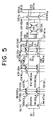
- Figure 5 is a circuit diagram showing a second embodiment of the semiconductor nonvolatile memory device according to the present invention.
- a NAND type flash memory two upper selective transistors are provided, one being made to act as a depletion transistor, whereby it is possible to adopt the folded bit line system.
- a dummy cell is used as a reference cell.
- this circuit has the same structure as that of the folded bit line of the well known DRAM circuit except the selective gate of each memory cell array is constituted by two stages.
- SA f denotes a flip-flop type sense amplifier 119 (in the same way as Fig. 3);
- BL denotes a bit line 100;
- BL_ denotes an inverted bit line 101;
- MCA 1h and MCA 2h denotes the memory cell arrays 107 and 102 connected to the bit line (BL) 100;
- MCA 1l and MCA 2l are memory cell arrays 108 and 103 connected to the inverted bit line (BL_) 101;
- DCL h denotes a dummy cell 95 connected to the bit line (BL 100;
- DCL l denotes a dummy cell 96 connected to the inverted bit line (BL_) 101;
- D denotes a data line 12;
- D_ denotes an inverted data line 125 taking a complementary level to that of the data line; and
- NT 11 to NT 16 denote nMOS transistors 93, 94, 116, 117, 123 and 124; respectively.
- Figure 6A and 6B are views showing an example of the structure of the memory cell array according to the present embodiment.
- each memory cell array is constituted by upper first and second selective transistors (SL 1 ) 133 and (SL 2 ) 135 connected in series; eight memory transistors (MT 0 to MT 7 ) 137, 139,..., 142 connected in series to the second selective transistor (SL 2 ) 135; and a lower selective transistor (SL 3 ) 144 connected in series between the memory transistor (MT 7 ) 142 and the ground.
- One of the first and second selective transistors (SL 1 ) 133 and (SL 2 ) 135 is constituted by a depletion transistor.
- the first selective transistor (SL 1 ) 133 is connected to the bit line (BL) 100 or the inverted bit line (BL_) 101.
- the first and second selective transistors (SL 1 ) 133 and (SL 2 ) 135 of the memory cell array connected to the same bit line (BL) 100 or inverted bit line (BL_) 101 are alternately constituted by the depletion transistor in an order of connection form the side of the sense amplifier SA f .
- the signals PC (92), SAG (115), and Y i (122) are set at the low level (0 V).
- the nMOS transistors (NT 11 to NT 16 ) 93, 94, 116, 117, 123, and 124 become the OFF state.
- the signals DSG and SG are set at the low level and the word line WL j and dummy word line (DWL) 97 are set at the high level (5 V).
- the VSAL (118) and VSAH (121) are set at the voltage V pc (91), and the data line (D) 126 and inverted data line (D_) 125 are set at (1/2) V CC level.
- the signals PC (92) and SAG (115) are set at the high level.
- the nMOS transistors (NT 11 to NT 14 ) 93, 94, 116 and 117 become the ON state.
- bit line (BL) 100 and inverted bit line (BL_) 101 are precharged to the voltage V pc (91).
- the word line of the almost simultaneously selected cell is set at the low level, and the signal SG is set at the high level.
- the signal DSG of the dummy cell DMC connected to the inverted bit line (BL_) 101 is set at the high level and the dummy word line (DWL) 97 is set at the low level.
- the signals SG 2 (110) and DSG 1 (99) are set at the high level, and the word line (WL) 100 and dummy word line (DWL) 97 are set at the low level.
- the signal PC (92) is set at the low level.
- the nMOS transistors (NT 11 and NT 12 ) 93 and 94 become the OFF state, and the sensing is started.
- the dummy cell DMC is set so as to pass a current at an intermediate level, the voltage V BL _ of the inverted bit line (BL_) 101 is slightly lowered.
- the signals SAG (115) and VSAL (118) are set to the low level and VSAH (121) is set to the high level.
- the voltage SA becomes the low level (0 V) and the voltage SA_ becomes the high level (5 V) due to the operation of the flip-flop-type sense amplifier SA f .
- the signal Y i (122) is set to the high level.
- the nMOS transistors (NT 15 and NT 16 ) 123 and 124 become the ON state and the voltages SA and SA_ are read out to the data line (D) 126 and the inverted data line (D_) 125.
- two selective transistors are used in each memory cell array and one selective transistor is made a depletion transistor, so it is possible to adopt a folded bit line system even in a NAND type flash memory.
- the layout is easy to set.
- various noise act in exactly the same way on the bit line (BL) 100 and the inverted bit line (BL_) 101. Therefore, the influence of the noise can be suppressed to the lowest level. Accordingly, it is possible to raise the sensitivity of the sense amplifier and to achieve an enhancement of speed.
- the cell size can be made smaller than a NOR type and the manufacturing process becomes simple as well.
- NAND type flash memory was explained as an example, but the present invention may also be applied to NOR type flash memory.
- the layout becomes easy and, further, various noise act in exactly the same way on the first and second bit lines, so the influence of noise can be suppressed to the lowest level. Accordingly, the sensitivity of the sense amplifier can be raised, and the enhancement of speed can be achieved.
Landscapes
- Read Only Memory (AREA)
- Semiconductor Memories (AREA)
Applications Claiming Priority (4)
| Application Number | Priority Date | Filing Date | Title |
|---|---|---|---|
| JP97306/93 | 1993-03-31 | ||
| JP9730693 | 1993-03-31 | ||
| JP9730693A JPH06290591A (ja) | 1993-03-31 | 1993-03-31 | 半導体不揮発性記憶装置 |
| EP94105067A EP0618589B1 (de) | 1993-03-31 | 1994-03-30 | Nichtflüchtige Speicheranordnung |
Related Parent Applications (1)
| Application Number | Title | Priority Date | Filing Date |
|---|---|---|---|
| EP94105067A Division EP0618589B1 (de) | 1993-03-31 | 1994-03-30 | Nichtflüchtige Speicheranordnung |
Publications (3)
| Publication Number | Publication Date |
|---|---|
| EP0834883A2 true EP0834883A2 (de) | 1998-04-08 |
| EP0834883A3 EP0834883A3 (de) | 1999-01-13 |
| EP0834883B1 EP0834883B1 (de) | 2001-07-25 |
Family
ID=14188812
Family Applications (2)
| Application Number | Title | Priority Date | Filing Date |
|---|---|---|---|
| EP97121071A Expired - Lifetime EP0834883B1 (de) | 1993-03-31 | 1994-03-30 | Nichtflüchtige Halbleiterspeicheranordnung |
| EP94105067A Expired - Lifetime EP0618589B1 (de) | 1993-03-31 | 1994-03-30 | Nichtflüchtige Speicheranordnung |
Family Applications After (1)
| Application Number | Title | Priority Date | Filing Date |
|---|---|---|---|
| EP94105067A Expired - Lifetime EP0618589B1 (de) | 1993-03-31 | 1994-03-30 | Nichtflüchtige Speicheranordnung |
Country Status (5)
| Country | Link |
|---|---|
| US (1) | US5459694A (de) |
| EP (2) | EP0834883B1 (de) |
| JP (1) | JPH06290591A (de) |
| KR (1) | KR940022570A (de) |
| DE (2) | DE69418521T2 (de) |
Families Citing this family (15)
| Publication number | Priority date | Publication date | Assignee | Title |
|---|---|---|---|---|
| US5761123A (en) * | 1995-06-13 | 1998-06-02 | Samsung Electronics, Co., Ltd. | Sense amplifier circuit of a nonvolatile semiconductor memory device |
| US5729493A (en) * | 1996-08-23 | 1998-03-17 | Motorola Inc. | Memory suitable for operation at low power supply voltages and sense amplifier therefor |
| KR100248868B1 (ko) * | 1996-12-14 | 2000-03-15 | 윤종용 | 플래시 불휘발성 반도체 메모리 장치 및 그 장치의 동작 모드 제어 방법 |
| KR100323554B1 (ko) | 1997-05-14 | 2002-03-08 | 니시무로 타이죠 | 불휘발성반도체메모리장치 |
| JP3359615B2 (ja) * | 1999-04-23 | 2002-12-24 | 松下電器産業株式会社 | 不揮発性半導体記憶装置 |
| US6188608B1 (en) | 1999-04-23 | 2001-02-13 | Matsushita Electric Industrial Co., Ltd. | Nonvolatile semiconductor memory device |
| JP2003157689A (ja) * | 2001-11-20 | 2003-05-30 | Hitachi Ltd | 半導体装置及びデータプロセッサ |
| JP4278438B2 (ja) * | 2003-05-27 | 2009-06-17 | 三洋電機株式会社 | 不揮発性半導体記憶装置及びその制御方法 |
| JP4484577B2 (ja) * | 2004-05-07 | 2010-06-16 | 株式会社ルネサステクノロジ | 半導体記憶装置及びその制御方法 |
| JP2006107546A (ja) * | 2004-09-30 | 2006-04-20 | Toshiba Corp | 不揮発性半導体記憶装置及びその動作方法 |
| JP4801986B2 (ja) * | 2005-02-03 | 2011-10-26 | 株式会社東芝 | 半導体記憶装置 |
| DE102007001783B4 (de) * | 2006-01-06 | 2018-03-29 | Samsung Electronics Co., Ltd. | Halbleiter-Speicherelement, Verfahren zum Schreiben oder Wiederherstellen einer Schwellspannung und zum Betreiben eines Halbleiter-Speicherelements |
| JP2010079953A (ja) * | 2008-09-24 | 2010-04-08 | Toshiba Corp | 半導体記憶装置 |
| KR101461632B1 (ko) | 2008-11-17 | 2014-11-13 | 삼성전자주식회사 | 계층적 비트 라인 구조를 가지는 반도체 메모리 장치 |
| JP5684161B2 (ja) * | 2012-01-26 | 2015-03-11 | 株式会社東芝 | 半導体装置 |
Family Cites Families (7)
| Publication number | Priority date | Publication date | Assignee | Title |
|---|---|---|---|---|
| US4305139A (en) * | 1979-12-26 | 1981-12-08 | International Business Machines Corporation | State detection for storage cells |
| US5022009A (en) * | 1988-06-02 | 1991-06-04 | Mitsubishi Denki Kabushiki Kaisha | Semiconductor memory device having reading operation of information by differential amplification |
| KR910004166B1 (ko) * | 1988-12-27 | 1991-06-22 | 삼성전자주식회사 | 낸드쎌들을 가지는 전기적으로 소거 및 프로그램 가능한 반도체 메모리장치 |
| JP2862584B2 (ja) * | 1989-08-31 | 1999-03-03 | 株式会社東芝 | 不揮発性半導体メモリ装置 |
| JPH04129092A (ja) * | 1990-09-18 | 1992-04-30 | Mitsubishi Electric Corp | 不揮発性半導体記憶装置 |
| JP2719237B2 (ja) * | 1990-12-20 | 1998-02-25 | シャープ株式会社 | ダイナミック型半導体記憶装置 |
| US5291045A (en) * | 1991-03-29 | 1994-03-01 | Kabushiki Kaisha Toshiba | Non-volatile semiconductor memory device using a differential cell in a memory cell |
-
1993
- 1993-03-31 JP JP9730693A patent/JPH06290591A/ja active Pending
-
1994
- 1994-03-29 US US08/219,542 patent/US5459694A/en not_active Expired - Fee Related
- 1994-03-29 KR KR1019940006326A patent/KR940022570A/ko not_active Withdrawn
- 1994-03-30 DE DE69418521T patent/DE69418521T2/de not_active Expired - Fee Related
- 1994-03-30 DE DE69427835T patent/DE69427835T2/de not_active Expired - Fee Related
- 1994-03-30 EP EP97121071A patent/EP0834883B1/de not_active Expired - Lifetime
- 1994-03-30 EP EP94105067A patent/EP0618589B1/de not_active Expired - Lifetime
Also Published As
| Publication number | Publication date |
|---|---|
| KR940022570A (ko) | 1994-10-21 |
| EP0834883A3 (de) | 1999-01-13 |
| EP0834883B1 (de) | 2001-07-25 |
| EP0618589A3 (en) | 1995-11-29 |
| DE69418521T2 (de) | 1999-11-18 |
| JPH06290591A (ja) | 1994-10-18 |
| DE69418521D1 (de) | 1999-06-24 |
| EP0618589A2 (de) | 1994-10-05 |
| EP0618589B1 (de) | 1999-05-19 |
| US5459694A (en) | 1995-10-17 |
| DE69427835D1 (de) | 2001-08-30 |
| DE69427835T2 (de) | 2002-04-04 |
Similar Documents
| Publication | Publication Date | Title |
|---|---|---|
| US5590073A (en) | Random access memory having flash memory | |
| KR0177776B1 (ko) | 고집적 반도체 메모리 장치의 데이타 센싱회로 | |
| US7436722B2 (en) | Semiconductor device | |
| US4841483A (en) | Semiconductor memory | |
| KR920008245B1 (ko) | 불휘발성 반도체기억장치 | |
| US5367488A (en) | DRAM having bidirectional global bit lines | |
| US6449201B1 (en) | Semiconductor memory device having a hierarchical bit line architecture | |
| US5459694A (en) | Nonvolatile storage apparatus with folded bit line structure | |
| US4654831A (en) | High speed CMOS current sense amplifier | |
| US6678198B2 (en) | Pseudo differential sensing method and apparatus for DRAM cell | |
| US6320806B1 (en) | Input/output line precharge circuit and semiconductor memory device adopting the same | |
| KR100242998B1 (ko) | 잡음특성을 개선한 셀 어레이 및 센스앰프의 구조 | |
| US4079462A (en) | Refreshing apparatus for MOS dynamic RAMs | |
| US4520466A (en) | Dynamic random access memory | |
| US4648073A (en) | Sequential shared access lines memory cells | |
| US4602355A (en) | Memory circuit with noise preventing means for word lines | |
| US4991142A (en) | Dynamic random access memory with improved sensing and refreshing | |
| US5515315A (en) | Dynamic random access memory | |
| EP1091359B1 (de) | Nichtfluechtiger halbleiterspeicher | |
| KR100318464B1 (ko) | 재쓰기회로를갖는스태틱램디바이스 | |
| JPS58147885A (ja) | ダイナミック型記憶装置 | |
| JPH0159680B2 (de) | ||
| JPH029084A (ja) | ダイナミックram | |
| JPS61148696A (ja) | 半導体記憶装置 | |
| KR20060022404A (ko) | 오픈 비트라인 구조를 갖는 반도체 메모리 장치 |
Legal Events
| Date | Code | Title | Description |
|---|---|---|---|
| PUAI | Public reference made under article 153(3) epc to a published international application that has entered the european phase |
Free format text: ORIGINAL CODE: 0009012 |
|
| 17P | Request for examination filed |
Effective date: 19971201 |
|
| AC | Divisional application: reference to earlier application |
Ref document number: 618589 Country of ref document: EP |
|
| AK | Designated contracting states |
Kind code of ref document: A2 Designated state(s): DE FR GB |
|
| PUAL | Search report despatched |
Free format text: ORIGINAL CODE: 0009013 |
|
| AK | Designated contracting states |
Kind code of ref document: A3 Designated state(s): DE FR GB |
|
| 17Q | First examination report despatched |
Effective date: 19991206 |
|
| GRAG | Despatch of communication of intention to grant |
Free format text: ORIGINAL CODE: EPIDOS AGRA |
|
| GRAG | Despatch of communication of intention to grant |
Free format text: ORIGINAL CODE: EPIDOS AGRA |
|
| GRAH | Despatch of communication of intention to grant a patent |
Free format text: ORIGINAL CODE: EPIDOS IGRA |
|
| DAX | Request for extension of the european patent (deleted) | ||
| GRAH | Despatch of communication of intention to grant a patent |
Free format text: ORIGINAL CODE: EPIDOS IGRA |
|
| GRAA | (expected) grant |
Free format text: ORIGINAL CODE: 0009210 |
|
| AC | Divisional application: reference to earlier application |
Ref document number: 618589 Country of ref document: EP |
|
| AK | Designated contracting states |
Kind code of ref document: B1 Designated state(s): DE FR GB |
|
| REF | Corresponds to: |
Ref document number: 69427835 Country of ref document: DE Date of ref document: 20010830 |
|
| EN | Fr: translation not filed | ||
| REG | Reference to a national code |
Ref country code: GB Ref legal event code: IF02 |
|
| PGFP | Annual fee paid to national office [announced via postgrant information from national office to epo] |
Ref country code: FR Payment date: 20020312 Year of fee payment: 9 |
|
| PGFP | Annual fee paid to national office [announced via postgrant information from national office to epo] |
Ref country code: GB Payment date: 20020327 Year of fee payment: 9 |
|
| PGFP | Annual fee paid to national office [announced via postgrant information from national office to epo] |
Ref country code: DE Payment date: 20020404 Year of fee payment: 9 |
|
| EN | Fr: translation not filed |
Free format text: BO 01/51 PAGES: 265, IL Y A LIEU DE SUPPRIMER: LA MENTION DE LA NON REMISE. LA REMISE EST PUBLIEE DANS LE PRESENT BOPI. |
|
| ET | Fr: translation filed | ||
| PLBE | No opposition filed within time limit |
Free format text: ORIGINAL CODE: 0009261 |
|
| 26N | No opposition filed | ||
| PG25 | Lapsed in a contracting state [announced via postgrant information from national office to epo] |
Ref country code: GB Free format text: LAPSE BECAUSE OF NON-PAYMENT OF DUE FEES Effective date: 20030330 |
|
| PG25 | Lapsed in a contracting state [announced via postgrant information from national office to epo] |
Ref country code: DE Free format text: LAPSE BECAUSE OF NON-PAYMENT OF DUE FEES Effective date: 20031001 |
|
| GBPC | Gb: european patent ceased through non-payment of renewal fee |
Effective date: 20030330 |
|
| PG25 | Lapsed in a contracting state [announced via postgrant information from national office to epo] |
Ref country code: FR Free format text: LAPSE BECAUSE OF NON-PAYMENT OF DUE FEES Effective date: 20031127 |
|
| REG | Reference to a national code |
Ref country code: FR Ref legal event code: ST |