EP0827631B1 - Verfahren zur strukturierung porösen siliciums - Google Patents
Verfahren zur strukturierung porösen siliciums Download PDFInfo
- Publication number
- EP0827631B1 EP0827631B1 EP96919582A EP96919582A EP0827631B1 EP 0827631 B1 EP0827631 B1 EP 0827631B1 EP 96919582 A EP96919582 A EP 96919582A EP 96919582 A EP96919582 A EP 96919582A EP 0827631 B1 EP0827631 B1 EP 0827631B1
- Authority
- EP
- European Patent Office
- Prior art keywords
- etching
- substrate
- silicon
- porosity
- voltage
- Prior art date
- Legal status (The legal status is an assumption and is not a legal conclusion. Google has not performed a legal analysis and makes no representation as to the accuracy of the status listed.)
- Expired - Lifetime
Links
Images



Classifications
-
- H—ELECTRICITY
- H10—SEMICONDUCTOR DEVICES; ELECTRIC SOLID-STATE DEVICES NOT OTHERWISE PROVIDED FOR
- H10P—GENERIC PROCESSES OR APPARATUS FOR THE MANUFACTURE OR TREATMENT OF DEVICES COVERED BY CLASS H10
- H10P50/00—Etching of wafers, substrates or parts of devices
-
- C—CHEMISTRY; METALLURGY
- C25—ELECTROLYTIC OR ELECTROPHORETIC PROCESSES; APPARATUS THEREFOR
- C25F—PROCESSES FOR THE ELECTROLYTIC REMOVAL OF MATERIALS FROM OBJECTS; APPARATUS THEREFOR
- C25F3/00—Electrolytic etching or polishing
- C25F3/02—Etching
- C25F3/14—Etching locally
-
- G—PHYSICS
- G02—OPTICS
- G02B—OPTICAL ELEMENTS, SYSTEMS OR APPARATUS
- G02B6/00—Light guides; Structural details of arrangements comprising light guides and other optical elements, e.g. couplings
- G02B6/10—Light guides; Structural details of arrangements comprising light guides and other optical elements, e.g. couplings of the optical waveguide type
- G02B6/12—Light guides; Structural details of arrangements comprising light guides and other optical elements, e.g. couplings of the optical waveguide type of the integrated circuit kind
- G02B6/122—Basic optical elements, e.g. light-guiding paths
-
- G—PHYSICS
- G02—OPTICS
- G02B—OPTICAL ELEMENTS, SYSTEMS OR APPARATUS
- G02B6/00—Light guides; Structural details of arrangements comprising light guides and other optical elements, e.g. couplings
- G02B6/10—Light guides; Structural details of arrangements comprising light guides and other optical elements, e.g. couplings of the optical waveguide type
- G02B6/12—Light guides; Structural details of arrangements comprising light guides and other optical elements, e.g. couplings of the optical waveguide type of the integrated circuit kind
- G02B6/13—Integrated optical circuits characterised by the manufacturing method
- G02B6/136—Integrated optical circuits characterised by the manufacturing method by etching
-
- G—PHYSICS
- G02—OPTICS
- G02B—OPTICAL ELEMENTS, SYSTEMS OR APPARATUS
- G02B6/00—Light guides; Structural details of arrangements comprising light guides and other optical elements, e.g. couplings
- G02B6/10—Light guides; Structural details of arrangements comprising light guides and other optical elements, e.g. couplings of the optical waveguide type
- G02B6/12—Light guides; Structural details of arrangements comprising light guides and other optical elements, e.g. couplings of the optical waveguide type of the integrated circuit kind
- G02B2006/12166—Manufacturing methods
- G02B2006/12173—Masking
-
- G—PHYSICS
- G02—OPTICS
- G02B—OPTICAL ELEMENTS, SYSTEMS OR APPARATUS
- G02B6/00—Light guides; Structural details of arrangements comprising light guides and other optical elements, e.g. couplings
- G02B6/10—Light guides; Structural details of arrangements comprising light guides and other optical elements, e.g. couplings of the optical waveguide type
- G02B6/12—Light guides; Structural details of arrangements comprising light guides and other optical elements, e.g. couplings of the optical waveguide type of the integrated circuit kind
- G02B2006/12166—Manufacturing methods
- G02B2006/12176—Etching
Definitions
- the invention relates to a method for structuring porous silicon according to the preamble of the claim 1.
- Porous silicon is due to its compatibility to advanced silicon (Si) microelectronics as well as its ease of manufacture a promising one Material for applications e.g. in the field of Optoelectronics as LEDs [W. Lang, P. Steiner and F. Kozlowski, "Optoelectronic properties of porous silicon.
- the electroluminescent devices ", in” Porous silicon science and technology ", Winter School Les Houches 1994, Springer Verlag Berlin Heidelberg New York], photodetector [J.P. Zheng, K.L. Jiao, W.P. Shen, W.A. Anderson and H.S. Kwok, Appl. Phys. Lett.
- US-A-4765865 discloses a method for etching Silicon at which the etch rate by applying a voltage is increased.
- the method according to the invention is concerned with influencing the etching depth and porosity profile of selectively etched PS structures and the control of the Undercutting the mask structure.
- a conductive or semiconductive layer e.g. made of metal or doped semiconductor
- the method according to the invention is concerned with influencing the etching depth and porosity profile of selectively etched PS structures and the control of the Undercutting the mask structure.
- a conductive or semiconductive layer e.g. made of metal or doped semiconductor
- an insulating layer e.g. made of photoresist, applied to the conductive layer become.
- the masking technique according to the invention also enables the control of undercutting the mask structure. For example, it is possible to underestimate the extent to reduce or a PS structure with a To coat layer of PS of other porosity, for example for waveguide applications.
- a substrate region 1 made of silicon with four trenches 5 made of porous silicon is shown in cross section in FIG. Above the substrate surface is an etching solution 4 which, when a voltage U PS is applied between it and the substrate 1, leads to the porosidization of the substrate regions 5 not shielded by photoresist 2 and in this way forms the trench structure 5.
- a structure with a substrate region 1 made of silicon and with four trenches 5 made of porous silicon is shown in cross section in FIG.
- a non-insulating layer 3 is provided on the areas of the substrate surface that are not intended for porosidization. This can be chosen to be metallic or semi-conductive and was applied to the voltage U M to the substrate 1.
- the photoresist 2 is applied to this layer 3, in particular to protect the layer 3. The photoresist 2 could be omitted if the non-insulating layer is sufficiently resistant to the etching solution 4 during the porosidization.
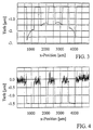
- FIG. 3 shows the result of an etching depth profile measurement of p-doped (2 ⁇ 10 15 cm -3 ), selectively anodized PS with the structure according to FIG. 1.
- the etched structure according to FIG. 1 consisted of four parallel strips, each 10 mm long and 0.50 mm wide, with a spacing of 0.50 mm each.
- the PS was removed with NaOH and the Etching depth profile measured with a surface profiler.
- the upper measurement shows the variation in the etching depth Using a conventional mask structure made of photoresist. The strong fluctuation is clearly recognizable of porosidation into the substrate within each of the trenches 5 and the large fluctuations and thus irregular partial etching from trench to trench.
- a mask structure made of 50 nm Cr, 400 nm Au and 1400 nm photoresist was used.
- the metal layers were alloyed in at 400 ° C. for 60 s.
- a desired profile can be set by specifically selecting the parameters. In particular, it is conceivable to place the five areas of the non-insulating layer 3 shown in FIG. 2, if necessary, at different voltages U M from one another for the duration of the etching for the porosidization of defined substrate areas.
- the roughness of the non-etched surface is caused by the alloyed metal.
- the etching depth is homogeneous over the entire structure.
- FIG. 5 shows a mask structure composed of a metal layer 3 and one Paint layer 2 as an insulator between metal 3 and Electrolyte 4.
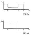
- the structuring can, for example with photolithography and lift-off technology or reactive Ion etching (RIE) take place. Can during the etching the applied voltages are kept constant or can be varied. The course over time is shown of the tensions and the resulting porosity profile for a waveguide structure.
- RIE reactive Ion etching
- a highly porous layer 5 was etched in the region 5 in order to form a waveguide in the substrate 1 in the period 0 ⁇ t ⁇ t 1 by applying a voltage U PS between the substrate 1 and the electrolyte 4 and thereby undercutting the metal mask 3 by applying it a voltage U M to the metal 3 prevented.
- the low-porosity core 6 was produced to form a waveguide 6, and undercutting was further prevented. Finally, a highly porous layer 7 was in turn etched for t 2 ⁇ t ⁇ t 3 to coat the core 6.
Landscapes
- Physics & Mathematics (AREA)
- Engineering & Computer Science (AREA)
- Microelectronics & Electronic Packaging (AREA)
- General Physics & Mathematics (AREA)
- Optics & Photonics (AREA)
- Chemical & Material Sciences (AREA)
- Chemical Kinetics & Catalysis (AREA)
- Electrochemistry (AREA)
- Materials Engineering (AREA)
- Metallurgy (AREA)
- Organic Chemistry (AREA)
- Optical Integrated Circuits (AREA)
- Weting (AREA)
- Treatments Of Macromolecular Shaped Articles (AREA)
Description
- Fig. 1:
- Struktur nach dem Stand der Technik;
- Fig. 2:
- erfindungsgemäßes Verfahren mit nicht-isolierender Schicht;
- Fig. 3:
- Ätztiefenprofil von selektiv anodisiertem PS nach Figur 1;
- Fig.4:
- Ätztiefenprofil von selektiv anodisiertem PS nach Figur 2;
- Fig. 5:
- Wellenleiter in PS;
- Fig. 6a:
- zeitliche Verlauf UPS;
- Fig. 6b:
- zeitliche Verlauf UM;
Claims (2)
- Verfahren zur Herstellung einer Struktur mit porösem Silicium, bei dem an der Oberfläche eines Siliciumsubstrats (1) mittels einer Ätzlösung (4) das Silicium porosidiert wird, wobei zwischen dem Substrat und der Ätzlösung zumindest während der Ätzung eine Spannung (UPS) angelegt wird,
dadurch gekennzeichnet, daß auf wenigstens einem nicht zur Porosidierung vorgesehenen Bereich der Substratoberfläche eine nicht-isolierende Schicht (3) aufgebracht wird und zwischen dieser Schicht und dem Substrat (1) während der Porosidierung eine elektrische Spannung (UM) angelegt wird. - Verfahren nach Anspruch 1,
dadurch gekennzeichnet, daß die Spannung (UM) zur Bildung von Bereichen unterschiedlicher Porosität zeitlich und/oder örtlich unterschiedlich eingestellt wird.
Applications Claiming Priority (3)
| Application Number | Priority Date | Filing Date | Title |
|---|---|---|---|
| DE19518371A DE19518371C1 (de) | 1995-05-22 | 1995-05-22 | Verfahren zur Strukturierung porösen Siliciums, sowie eine poröses Silicium enthaltende Struktur |
| DE19518371 | 1995-05-22 | ||
| PCT/DE1996/000913 WO1996037911A1 (de) | 1995-05-22 | 1996-05-20 | Verfahren zur strukturierung porösen siliciums, sowie eine poröses silicium enthaltende struktur |
Publications (2)
| Publication Number | Publication Date |
|---|---|
| EP0827631A1 EP0827631A1 (de) | 1998-03-11 |
| EP0827631B1 true EP0827631B1 (de) | 2002-07-24 |
Family
ID=7762320
Family Applications (1)
| Application Number | Title | Priority Date | Filing Date |
|---|---|---|---|
| EP96919582A Expired - Lifetime EP0827631B1 (de) | 1995-05-22 | 1996-05-20 | Verfahren zur strukturierung porösen siliciums |
Country Status (4)
| Country | Link |
|---|---|
| EP (1) | EP0827631B1 (de) |
| AT (1) | ATE221253T1 (de) |
| DE (2) | DE19518371C1 (de) |
| WO (1) | WO1996037911A1 (de) |
Cited By (1)
| Publication number | Priority date | Publication date | Assignee | Title |
|---|---|---|---|---|
| CN103258718A (zh) * | 2013-05-16 | 2013-08-21 | 华北电力大学 | 一种基于lsp效应制备“弹坑状”多孔硅结构的方法 |
Families Citing this family (14)
| Publication number | Priority date | Publication date | Assignee | Title |
|---|---|---|---|---|
| DE19700982A1 (de) * | 1997-01-14 | 1998-07-16 | Siemens Ag | Verfahren zur Bildung von Lochstrukturen in einem Siliziumsubstrat |
| DE19743692A1 (de) * | 1997-10-02 | 1999-04-08 | Zae Bayern | Multifunktionsschicht zur Verbesserung des Wirkungsgrades von kristallinen Dünnschicht Silizium Solarzellen |
| DE19757321A1 (de) * | 1997-12-23 | 1999-07-01 | Forschungszentrum Juelich Gmbh | Optische Komponente und Verwendung einer Beschichtung für eine solche Komponente |
| DE19757560A1 (de) * | 1997-12-23 | 1999-07-01 | Forschungszentrum Juelich Gmbh | Verfahren zur Herstellung einer porösen Schicht mit Hilfe eines elektrochemischen Ätzprozesses |
| DE19837126B4 (de) * | 1998-08-17 | 2004-02-05 | Forschungszentrum Jülich GmbH | Verfahren und Vorrichtung zur elektrischen oder elektrochemischen Manipulation von Proben |
| DE19921190A1 (de) * | 1999-05-07 | 2000-11-16 | Forschungszentrum Juelich Gmbh | Verfahren zur Herstellung eines Elements mit porosidiertem Material |
| US6277662B1 (en) | 1999-06-03 | 2001-08-21 | Seiichi Nagata | Silicon substrate and forming method thereof |
| DE10036724A1 (de) * | 2000-07-27 | 2002-02-14 | Infineon Technologies Ag | Verfahren zur Bildung eines Grabens in einem Halbleitersubstrat |
| DE10046622B4 (de) * | 2000-09-20 | 2010-05-20 | Robert Bosch Gmbh | Verfahren zur Herstellung einer Membransensoreinheit sowie Membransensoreinheit |
| DE10055872B4 (de) * | 2000-11-10 | 2004-02-05 | Robert Bosch Gmbh | Verfahren zur Herstellung einer porösen Struktur für ein Sieb oder einen Filter und poröse Struktur für ein Sieb oder einen Filter |
| DE10117486A1 (de) * | 2001-04-07 | 2002-10-17 | Bosch Gmbh Robert | Verfahren zur Herstelung eines Halbleiterbauelements sowie ein nach dem Verfahren hergestelltes Halbleiterbauelement |
| US7231123B2 (en) | 2003-12-26 | 2007-06-12 | Canon Kabushiki Kaisha | Photonic crystal optical element and manufacturing method therefor |
| EP4579296A1 (de) | 2023-12-29 | 2025-07-02 | Université catholique de Louvain | Integrierte terahertz-schaltkreisvorrichtung und verfahren zu ihrer herstellung |
| DE102024204316A1 (de) * | 2024-05-08 | 2025-11-13 | Robert Bosch Gesellschaft mit beschränkter Haftung | Verfahren zum Herstellen einer Struktur in einem Halbleitersubstrat |
Family Cites Families (6)
| Publication number | Priority date | Publication date | Assignee | Title |
|---|---|---|---|---|
| US3929529A (en) * | 1974-12-09 | 1975-12-30 | Ibm | Method for gettering contaminants in monocrystalline silicon |
| US3962052A (en) * | 1975-04-14 | 1976-06-08 | International Business Machines Corporation | Process for forming apertures in silicon bodies |
| DE3068851D1 (en) * | 1979-05-02 | 1984-09-13 | Ibm | Apparatus and process for selective electrochemical etching |
| US4765865A (en) * | 1987-05-04 | 1988-08-23 | Ford Motor Company | Silicon etch rate enhancement |
| EP0563625A3 (en) * | 1992-04-03 | 1994-05-25 | Ibm | Immersion scanning system for fabricating porous silicon films and devices |
| KR970007786B1 (ko) * | 1993-11-08 | 1997-05-16 | 이종덕 | 실리콘 필드 에미터 어레이의 제조방법 |
-
1995
- 1995-05-22 DE DE19518371A patent/DE19518371C1/de not_active Expired - Fee Related
-
1996
- 1996-05-20 AT AT96919582T patent/ATE221253T1/de not_active IP Right Cessation
- 1996-05-20 WO PCT/DE1996/000913 patent/WO1996037911A1/de not_active Ceased
- 1996-05-20 DE DE59609486T patent/DE59609486D1/de not_active Expired - Fee Related
- 1996-05-20 EP EP96919582A patent/EP0827631B1/de not_active Expired - Lifetime
Cited By (2)
| Publication number | Priority date | Publication date | Assignee | Title |
|---|---|---|---|---|
| CN103258718A (zh) * | 2013-05-16 | 2013-08-21 | 华北电力大学 | 一种基于lsp效应制备“弹坑状”多孔硅结构的方法 |
| CN103258718B (zh) * | 2013-05-16 | 2015-10-21 | 华北电力大学 | 一种基于lsp效应制备“弹坑状”多孔硅结构的方法 |
Also Published As
| Publication number | Publication date |
|---|---|
| ATE221253T1 (de) | 2002-08-15 |
| EP0827631A1 (de) | 1998-03-11 |
| DE19518371C1 (de) | 1996-10-24 |
| WO1996037911A1 (de) | 1996-11-28 |
| DE59609486D1 (de) | 2002-08-29 |
Similar Documents
| Publication | Publication Date | Title |
|---|---|---|
| DE3936694C2 (de) | Halbleiterbauteil, insbesondere DFB-Halbleiterlaser | |
| DE19518371C1 (de) | Verfahren zur Strukturierung porösen Siliciums, sowie eine poröses Silicium enthaltende Struktur | |
| DE69019530T2 (de) | Mikromechanischer schalter. | |
| EP0553464B1 (de) | Verfahren zur Herstellung einer Solarzelle aus einer Substratscheibe | |
| DE3300131C2 (de) | Integriertes optisches Bauelement und Verfahren zu seiner Herstellung | |
| EP0010596A1 (de) | Verfahren zur Ausbildung von Maskenöffnungen bei der Herstellung von Halbleiteranordnungen | |
| DE19545164A1 (de) | Optische Halbleitervorrichtung und Herstellungsverfahren dafür | |
| EP1167934A1 (de) | Mikromechanisches Bauelement, insbesondere Sensorelement, mit einer stabilisierten Membran und Verfahren zur Herstellung eines derartigen Bauelementes | |
| DE2812658C3 (de) | Verfahren zum selektiven Diffundieren von Aluminium in ein Einkristall-Siliciumhalbleitersubstrat | |
| DE69333843T2 (de) | Ätzverfahren für Silizium-Substrat | |
| EP0946890B1 (de) | Schicht mit porösem schichtbereich, eine solche schicht enthaltendes interferenzfilter sowie verfahren zu ihrer herstellung | |
| DE19843984A1 (de) | Verfahren zur Herstellung eines Strahlungssensors | |
| DE4010889C2 (de) | ||
| DE19527314A1 (de) | Siliziummembran und Verfahren zur Herstellung einer Siliziummembran | |
| DE3634140C2 (de) | ||
| EP1198844B1 (de) | Diode mit metall-halbleiterkontakt und verfahren zu ihrer herstellung | |
| DE69216061T2 (de) | Organische Feldeffekt-Schaltanordnung | |
| DE3128982C2 (de) | Verfahren zur Herstellung mindestens eines Josephson-Tunnelelementes | |
| DE3886751T2 (de) | Methode zum Ätzen von Spiegelfacetten an III-V-Halbleiterstrukturen. | |
| EP1284024A1 (de) | Bauelement für die optoelektronik und verfahren zu dessen herstellung | |
| DE60203840T2 (de) | Halbleiterlaser und Herstellungsverfahren | |
| DE4432010C2 (de) | Optische Schaltvorrichtung und Herstellungsverfahren für diese | |
| EP1042794A1 (de) | Verfahren zur herstellung einer porösen schicht mit hilfe eines elektrochemischen ätzprozesses | |
| DE102007051725B4 (de) | Verfahren zur Kontaktierung von Solarzellen | |
| EP0479837A1 (de) | Verfahren zum herstellen eines verlustarmen, optischen wellenleiters in einer epitaktischen silizium-schicht |
Legal Events
| Date | Code | Title | Description |
|---|---|---|---|
| PUAI | Public reference made under article 153(3) epc to a published international application that has entered the european phase |
Free format text: ORIGINAL CODE: 0009012 |
|
| 17P | Request for examination filed |
Effective date: 19971121 |
|
| AK | Designated contracting states |
Kind code of ref document: A1 Designated state(s): AT DE FR GB NL |
|
| 17Q | First examination report despatched |
Effective date: 19981113 |
|
| RTI1 | Title (correction) |
Free format text: PROCESS FOR STRUCTURING POROUS SILICON |
|
| RTI1 | Title (correction) |
Free format text: PROCESS FOR STRUCTURING POROUS SILICON |
|
| GRAG | Despatch of communication of intention to grant |
Free format text: ORIGINAL CODE: EPIDOS AGRA |
|
| GRAG | Despatch of communication of intention to grant |
Free format text: ORIGINAL CODE: EPIDOS AGRA |
|
| GRAH | Despatch of communication of intention to grant a patent |
Free format text: ORIGINAL CODE: EPIDOS IGRA |
|
| GRAH | Despatch of communication of intention to grant a patent |
Free format text: ORIGINAL CODE: EPIDOS IGRA |
|
| GRAA | (expected) grant |
Free format text: ORIGINAL CODE: 0009210 |
|
| RAP1 | Party data changed (applicant data changed or rights of an application transferred) |
Owner name: FORSCHUNGSZENTRUM JUELICH GMBH |
|
| AK | Designated contracting states |
Kind code of ref document: B1 Designated state(s): AT DE FR GB NL |
|
| PG25 | Lapsed in a contracting state [announced via postgrant information from national office to epo] |
Ref country code: NL Free format text: LAPSE BECAUSE OF FAILURE TO SUBMIT A TRANSLATION OF THE DESCRIPTION OR TO PAY THE FEE WITHIN THE PRESCRIBED TIME-LIMIT Effective date: 20020724 Ref country code: GB Free format text: LAPSE BECAUSE OF FAILURE TO SUBMIT A TRANSLATION OF THE DESCRIPTION OR TO PAY THE FEE WITHIN THE PRESCRIBED TIME-LIMIT Effective date: 20020724 Ref country code: FR Free format text: LAPSE BECAUSE OF NON-PAYMENT OF DUE FEES Effective date: 20020724 |
|
| REF | Corresponds to: |
Ref document number: 221253 Country of ref document: AT Date of ref document: 20020815 Kind code of ref document: T |
|
| REG | Reference to a national code |
Ref country code: GB Ref legal event code: FG4D Free format text: NOT ENGLISH |
|
| REF | Corresponds to: |
Ref document number: 59609486 Country of ref document: DE Date of ref document: 20020829 |
|
| NLV1 | Nl: lapsed or annulled due to failure to fulfill the requirements of art. 29p and 29m of the patents act | ||
| GBV | Gb: ep patent (uk) treated as always having been void in accordance with gb section 77(7)/1977 [no translation filed] |
Effective date: 20020724 |
|
| EN | Fr: translation not filed | ||
| PG25 | Lapsed in a contracting state [announced via postgrant information from national office to epo] |
Ref country code: AT Free format text: LAPSE BECAUSE OF NON-PAYMENT OF DUE FEES Effective date: 20030520 |
|
| PLBE | No opposition filed within time limit |
Free format text: ORIGINAL CODE: 0009261 |
|
| STAA | Information on the status of an ep patent application or granted ep patent |
Free format text: STATUS: NO OPPOSITION FILED WITHIN TIME LIMIT |
|
| 26N | No opposition filed |
Effective date: 20030425 |
|
| PG25 | Lapsed in a contracting state [announced via postgrant information from national office to epo] |
Ref country code: DE Free format text: LAPSE BECAUSE OF NON-PAYMENT OF DUE FEES Effective date: 20031202 |