EP0827166A1 - Vielschichtkondensator mit Wolfram-haltigem Batio3 - Google Patents
Vielschichtkondensator mit Wolfram-haltigem Batio3 Download PDFInfo
- Publication number
- EP0827166A1 EP0827166A1 EP97202578A EP97202578A EP0827166A1 EP 0827166 A1 EP0827166 A1 EP 0827166A1 EP 97202578 A EP97202578 A EP 97202578A EP 97202578 A EP97202578 A EP 97202578A EP 0827166 A1 EP0827166 A1 EP 0827166A1
- Authority
- EP
- European Patent Office
- Prior art keywords
- mol
- dielectric
- nickel
- formula unit
- electrodes
- Prior art date
- Legal status (The legal status is an assumption and is not a legal conclusion. Google has not performed a legal analysis and makes no representation as to the accuracy of the status listed.)
- Withdrawn
Links
- 239000003990 capacitor Substances 0.000 title claims abstract description 55
- WFKWXMTUELFFGS-UHFFFAOYSA-N tungsten Chemical group [W] WFKWXMTUELFFGS-UHFFFAOYSA-N 0.000 title claims abstract description 13
- 229910052721 tungsten Inorganic materials 0.000 title claims abstract description 13
- 239000010937 tungsten Substances 0.000 title claims abstract description 13
- 229910002113 barium titanate Inorganic materials 0.000 title description 4
- PXHVJJICTQNCMI-UHFFFAOYSA-N Nickel Chemical compound [Ni] PXHVJJICTQNCMI-UHFFFAOYSA-N 0.000 claims abstract description 42
- 239000000203 mixture Substances 0.000 claims abstract description 40
- 239000000919 ceramic Substances 0.000 claims abstract description 36
- 229910052759 nickel Inorganic materials 0.000 claims abstract description 21
- RTAQQCXQSZGOHL-UHFFFAOYSA-N Titanium Chemical compound [Ti] RTAQQCXQSZGOHL-UHFFFAOYSA-N 0.000 claims abstract description 13
- 239000000463 material Substances 0.000 claims abstract description 13
- 238000002360 preparation method Methods 0.000 claims abstract description 12
- VYPSYNLAJGMNEJ-UHFFFAOYSA-N Silicium dioxide Chemical compound O=[Si]=O VYPSYNLAJGMNEJ-UHFFFAOYSA-N 0.000 claims abstract description 10
- 229910052727 yttrium Inorganic materials 0.000 claims abstract description 8
- VWQVUPCCIRVNHF-UHFFFAOYSA-N yttrium atom Chemical compound [Y] VWQVUPCCIRVNHF-UHFFFAOYSA-N 0.000 claims abstract description 8
- 229910000990 Ni alloy Inorganic materials 0.000 claims abstract description 6
- HCHKCACWOHOZIP-UHFFFAOYSA-N Zinc Chemical compound [Zn] HCHKCACWOHOZIP-UHFFFAOYSA-N 0.000 claims abstract description 5
- 229910052725 zinc Inorganic materials 0.000 claims abstract description 5
- 239000011701 zinc Substances 0.000 claims abstract description 5
- 229910052769 Ytterbium Inorganic materials 0.000 claims abstract description 4
- 229910052782 aluminium Inorganic materials 0.000 claims abstract description 4
- XAGFODPZIPBFFR-UHFFFAOYSA-N aluminium Chemical compound [Al] XAGFODPZIPBFFR-UHFFFAOYSA-N 0.000 claims abstract description 4
- FUJCRWPEOMXPAD-UHFFFAOYSA-N lithium oxide Chemical compound [Li+].[Li+].[O-2] FUJCRWPEOMXPAD-UHFFFAOYSA-N 0.000 claims abstract description 4
- 229910001947 lithium oxide Inorganic materials 0.000 claims abstract description 4
- 229910052814 silicon oxide Inorganic materials 0.000 claims abstract description 4
- NAWDYIZEMPQZHO-UHFFFAOYSA-N ytterbium Chemical compound [Yb] NAWDYIZEMPQZHO-UHFFFAOYSA-N 0.000 claims abstract description 4
- GYHNNYVSQQEPJS-UHFFFAOYSA-N Gallium Chemical compound [Ga] GYHNNYVSQQEPJS-UHFFFAOYSA-N 0.000 claims abstract description 3
- 229910052733 gallium Inorganic materials 0.000 claims abstract description 3
- 238000005245 sintering Methods 0.000 claims description 35
- 239000011575 calcium Substances 0.000 claims description 10
- LVZCQZOALBUKMO-UHFFFAOYSA-N [Zr].[Ca].[Ba] Chemical compound [Zr].[Ca].[Ba] LVZCQZOALBUKMO-UHFFFAOYSA-N 0.000 claims description 8
- FQNGWRSKYZLJDK-UHFFFAOYSA-N [Ca].[Ba] Chemical compound [Ca].[Ba] FQNGWRSKYZLJDK-UHFFFAOYSA-N 0.000 abstract description 3
- 229910052845 zircon Inorganic materials 0.000 abstract description 3
- GFQYVLUOOAAOGM-UHFFFAOYSA-N zirconium(iv) silicate Chemical compound [Zr+4].[O-][Si]([O-])([O-])[O-] GFQYVLUOOAAOGM-UHFFFAOYSA-N 0.000 abstract description 3
- 239000004411 aluminium Substances 0.000 abstract 1
- 238000000034 method Methods 0.000 description 22
- 238000000227 grinding Methods 0.000 description 18
- IJGRMHOSHXDMSA-UHFFFAOYSA-N Atomic nitrogen Chemical compound N#N IJGRMHOSHXDMSA-UHFFFAOYSA-N 0.000 description 16
- 229910004298 SiO 2 Inorganic materials 0.000 description 15
- 238000004519 manufacturing process Methods 0.000 description 15
- 229910052757 nitrogen Inorganic materials 0.000 description 14
- XLYOFNOQVPJJNP-UHFFFAOYSA-N water Substances O XLYOFNOQVPJJNP-UHFFFAOYSA-N 0.000 description 14
- 238000005496 tempering Methods 0.000 description 13
- KFZMGEQAYNKOFK-UHFFFAOYSA-N Isopropanol Chemical compound CC(C)O KFZMGEQAYNKOFK-UHFFFAOYSA-N 0.000 description 12
- 239000007789 gas Substances 0.000 description 12
- 239000010936 titanium Substances 0.000 description 12
- QVGXLLKOCUKJST-UHFFFAOYSA-N atomic oxygen Chemical compound [O] QVGXLLKOCUKJST-UHFFFAOYSA-N 0.000 description 11
- 239000001301 oxygen Substances 0.000 description 11
- 229910052760 oxygen Inorganic materials 0.000 description 11
- 239000012298 atmosphere Substances 0.000 description 10
- 239000000725 suspension Substances 0.000 description 10
- 239000011230 binding agent Substances 0.000 description 8
- 239000002270 dispersing agent Substances 0.000 description 8
- 239000010931 gold Substances 0.000 description 8
- 239000011572 manganese Substances 0.000 description 8
- BASFCYQUMIYNBI-UHFFFAOYSA-N platinum Chemical compound [Pt] BASFCYQUMIYNBI-UHFFFAOYSA-N 0.000 description 8
- 239000004372 Polyvinyl alcohol Substances 0.000 description 7
- 229910052739 hydrogen Inorganic materials 0.000 description 7
- 238000009413 insulation Methods 0.000 description 7
- 229910052751 metal Inorganic materials 0.000 description 7
- 239000002184 metal Substances 0.000 description 7
- 229920002451 polyvinyl alcohol Polymers 0.000 description 7
- 229920006395 saturated elastomer Polymers 0.000 description 7
- XDTMQSROBMDMFD-UHFFFAOYSA-N Cyclohexane Chemical compound C1CCCCC1 XDTMQSROBMDMFD-UHFFFAOYSA-N 0.000 description 6
- 101100513612 Microdochium nivale MnCO gene Proteins 0.000 description 6
- 229910010413 TiO 2 Inorganic materials 0.000 description 6
- 239000012530 fluid Substances 0.000 description 6
- 238000010438 heat treatment Methods 0.000 description 6
- 239000004094 surface-active agent Substances 0.000 description 6
- 239000010953 base metal Substances 0.000 description 5
- 239000003985 ceramic capacitor Substances 0.000 description 5
- 150000001875 compounds Chemical class 0.000 description 5
- 230000001590 oxidative effect Effects 0.000 description 5
- KDLHZDBZIXYQEI-UHFFFAOYSA-N Palladium Chemical compound [Pd] KDLHZDBZIXYQEI-UHFFFAOYSA-N 0.000 description 4
- 229910052697 platinum Inorganic materials 0.000 description 4
- 239000000843 powder Substances 0.000 description 4
- YXFVVABEGXRONW-UHFFFAOYSA-N Toluene Chemical compound CC1=CC=CC=C1 YXFVVABEGXRONW-UHFFFAOYSA-N 0.000 description 3
- 239000000370 acceptor Substances 0.000 description 3
- JRPBQTZRNDNNOP-UHFFFAOYSA-N barium titanate Chemical compound [Ba+2].[Ba+2].[O-][Ti]([O-])([O-])[O-] JRPBQTZRNDNNOP-UHFFFAOYSA-N 0.000 description 3
- 229910052703 rhodium Inorganic materials 0.000 description 3
- 239000010948 rhodium Substances 0.000 description 3
- MHOVAHRLVXNVSD-UHFFFAOYSA-N rhodium atom Chemical compound [Rh] MHOVAHRLVXNVSD-UHFFFAOYSA-N 0.000 description 3
- 239000002904 solvent Substances 0.000 description 3
- 229910052719 titanium Inorganic materials 0.000 description 3
- PEDCQBHIVMGVHV-UHFFFAOYSA-N Glycerine Chemical compound OCC(O)CO PEDCQBHIVMGVHV-UHFFFAOYSA-N 0.000 description 2
- XEEYBQQBJWHFJM-UHFFFAOYSA-N Iron Chemical compound [Fe] XEEYBQQBJWHFJM-UHFFFAOYSA-N 0.000 description 2
- 229910045601 alloy Inorganic materials 0.000 description 2
- 239000000956 alloy Substances 0.000 description 2
- 238000005266 casting Methods 0.000 description 2
- 239000011651 chromium Substances 0.000 description 2
- 239000013078 crystal Substances 0.000 description 2
- 238000001704 evaporation Methods 0.000 description 2
- 238000010304 firing Methods 0.000 description 2
- PCHJSUWPFVWCPO-UHFFFAOYSA-N gold Chemical compound [Au] PCHJSUWPFVWCPO-UHFFFAOYSA-N 0.000 description 2
- 229910052737 gold Inorganic materials 0.000 description 2
- AMWRITDGCCNYAT-UHFFFAOYSA-L hydroxy(oxo)manganese;manganese Chemical compound [Mn].O[Mn]=O.O[Mn]=O AMWRITDGCCNYAT-UHFFFAOYSA-L 0.000 description 2
- WPBNNNQJVZRUHP-UHFFFAOYSA-L manganese(2+);methyl n-[[2-(methoxycarbonylcarbamothioylamino)phenyl]carbamothioyl]carbamate;n-[2-(sulfidocarbothioylamino)ethyl]carbamodithioate Chemical compound [Mn+2].[S-]C(=S)NCCNC([S-])=S.COC(=O)NC(=S)NC1=CC=CC=C1NC(=S)NC(=O)OC WPBNNNQJVZRUHP-UHFFFAOYSA-L 0.000 description 2
- 229910052763 palladium Inorganic materials 0.000 description 2
- 239000004014 plasticizer Substances 0.000 description 2
- 238000007493 shaping process Methods 0.000 description 2
- GLDUZMNCEGHSBP-UHFFFAOYSA-N 2-(2-octylphenoxy)ethanol Chemical compound CCCCCCCCC1=CC=CC=C1OCCO GLDUZMNCEGHSBP-UHFFFAOYSA-N 0.000 description 1
- ZNQVEEAIQZEUHB-UHFFFAOYSA-N 2-ethoxyethanol Chemical compound CCOCCO ZNQVEEAIQZEUHB-UHFFFAOYSA-N 0.000 description 1
- VYZAMTAEIAYCRO-UHFFFAOYSA-N Chromium Chemical compound [Cr] VYZAMTAEIAYCRO-UHFFFAOYSA-N 0.000 description 1
- RYGMFSIKBFXOCR-UHFFFAOYSA-N Copper Chemical compound [Cu] RYGMFSIKBFXOCR-UHFFFAOYSA-N 0.000 description 1
- LFQSCWFLJHTTHZ-UHFFFAOYSA-N Ethanol Chemical compound CCO LFQSCWFLJHTTHZ-UHFFFAOYSA-N 0.000 description 1
- UFHFLCQGNIYNRP-UHFFFAOYSA-N Hydrogen Chemical compound [H][H] UFHFLCQGNIYNRP-UHFFFAOYSA-N 0.000 description 1
- ZOKXTWBITQBERF-UHFFFAOYSA-N Molybdenum Chemical compound [Mo] ZOKXTWBITQBERF-UHFFFAOYSA-N 0.000 description 1
- CTQNGGLPUBDAKN-UHFFFAOYSA-N O-Xylene Chemical compound CC1=CC=CC=C1C CTQNGGLPUBDAKN-UHFFFAOYSA-N 0.000 description 1
- 239000002202 Polyethylene glycol Substances 0.000 description 1
- 239000004721 Polyphenylene oxide Substances 0.000 description 1
- BQCADISMDOOEFD-UHFFFAOYSA-N Silver Chemical compound [Ag] BQCADISMDOOEFD-UHFFFAOYSA-N 0.000 description 1
- ATJFFYVFTNAWJD-UHFFFAOYSA-N Tin Chemical compound [Sn] ATJFFYVFTNAWJD-UHFFFAOYSA-N 0.000 description 1
- XSTXAVWGXDQKEL-UHFFFAOYSA-N Trichloroethylene Chemical group ClC=C(Cl)Cl XSTXAVWGXDQKEL-UHFFFAOYSA-N 0.000 description 1
- QCWXUUIWCKQGHC-UHFFFAOYSA-N Zirconium Chemical compound [Zr] QCWXUUIWCKQGHC-UHFFFAOYSA-N 0.000 description 1
- XHCLAFWTIXFWPH-UHFFFAOYSA-N [O-2].[O-2].[O-2].[O-2].[O-2].[V+5].[V+5] Chemical compound [O-2].[O-2].[O-2].[O-2].[O-2].[V+5].[V+5] XHCLAFWTIXFWPH-UHFFFAOYSA-N 0.000 description 1
- 150000001242 acetic acid derivatives Chemical class 0.000 description 1
- 239000000654 additive Substances 0.000 description 1
- 150000001298 alcohols Chemical class 0.000 description 1
- 150000004703 alkoxides Chemical class 0.000 description 1
- 125000002877 alkyl aryl group Chemical group 0.000 description 1
- 230000015572 biosynthetic process Effects 0.000 description 1
- 150000004649 carbonic acid derivatives Chemical class 0.000 description 1
- 230000015556 catabolic process Effects 0.000 description 1
- 229910052804 chromium Inorganic materials 0.000 description 1
- 238000000975 co-precipitation Methods 0.000 description 1
- 229910017052 cobalt Inorganic materials 0.000 description 1
- 239000010941 cobalt Substances 0.000 description 1
- GUTLYIVDDKVIGB-UHFFFAOYSA-N cobalt atom Chemical compound [Co] GUTLYIVDDKVIGB-UHFFFAOYSA-N 0.000 description 1
- 229910052802 copper Inorganic materials 0.000 description 1
- 239000010949 copper Substances 0.000 description 1
- 230000008878 coupling Effects 0.000 description 1
- 238000010168 coupling process Methods 0.000 description 1
- 238000005859 coupling reaction Methods 0.000 description 1
- 238000006731 degradation reaction Methods 0.000 description 1
- 239000003989 dielectric material Substances 0.000 description 1
- 230000005684 electric field Effects 0.000 description 1
- 239000007772 electrode material Substances 0.000 description 1
- 238000005516 engineering process Methods 0.000 description 1
- 230000008020 evaporation Effects 0.000 description 1
- 235000011187 glycerol Nutrition 0.000 description 1
- 239000001257 hydrogen Substances 0.000 description 1
- 150000004679 hydroxides Chemical class 0.000 description 1
- 150000002500 ions Chemical class 0.000 description 1
- 229910052742 iron Inorganic materials 0.000 description 1
- 239000011133 lead Substances 0.000 description 1
- 238000005259 measurement Methods 0.000 description 1
- 150000002739 metals Chemical class 0.000 description 1
- 229910052750 molybdenum Inorganic materials 0.000 description 1
- 239000011733 molybdenum Substances 0.000 description 1
- QGLKJKCYBOYXKC-UHFFFAOYSA-N nonaoxidotritungsten Chemical compound O=[W]1(=O)O[W](=O)(=O)O[W](=O)(=O)O1 QGLKJKCYBOYXKC-UHFFFAOYSA-N 0.000 description 1
- 229920000620 organic polymer Polymers 0.000 description 1
- 150000003891 oxalate salts Chemical class 0.000 description 1
- 230000003647 oxidation Effects 0.000 description 1
- 238000007254 oxidation reaction Methods 0.000 description 1
- SIWVEOZUMHYXCS-UHFFFAOYSA-N oxo(oxoyttriooxy)yttrium Chemical compound O=[Y]O[Y]=O SIWVEOZUMHYXCS-UHFFFAOYSA-N 0.000 description 1
- 125000005498 phthalate group Chemical class 0.000 description 1
- 239000006187 pill Substances 0.000 description 1
- 229920002037 poly(vinyl butyral) polymer Polymers 0.000 description 1
- 229920000570 polyether Polymers 0.000 description 1
- 229920001223 polyethylene glycol Polymers 0.000 description 1
- 229920000151 polyglycol Polymers 0.000 description 1
- 239000010695 polyglycol Substances 0.000 description 1
- 239000010970 precious metal Substances 0.000 description 1
- 238000006479 redox reaction Methods 0.000 description 1
- 238000006722 reduction reaction Methods 0.000 description 1
- 238000007650 screen-printing Methods 0.000 description 1
- 229910052709 silver Inorganic materials 0.000 description 1
- 239000004332 silver Substances 0.000 description 1
- 238000001694 spray drying Methods 0.000 description 1
- 239000000126 substance Substances 0.000 description 1
- 230000001629 suppression Effects 0.000 description 1
- 229910052718 tin Inorganic materials 0.000 description 1
- 239000011135 tin Substances 0.000 description 1
- 229910001930 tungsten oxide Inorganic materials 0.000 description 1
- 229910052720 vanadium Inorganic materials 0.000 description 1
- GPPXJZIENCGNKB-UHFFFAOYSA-N vanadium Chemical compound [V]#[V] GPPXJZIENCGNKB-UHFFFAOYSA-N 0.000 description 1
- 229910001935 vanadium oxide Inorganic materials 0.000 description 1
- 239000008096 xylene Substances 0.000 description 1
- 229910052726 zirconium Inorganic materials 0.000 description 1
Images
Classifications
-
- H—ELECTRICITY
- H01—ELECTRIC ELEMENTS
- H01G—CAPACITORS; CAPACITORS, RECTIFIERS, DETECTORS, SWITCHING DEVICES, LIGHT-SENSITIVE OR TEMPERATURE-SENSITIVE DEVICES OF THE ELECTROLYTIC TYPE
- H01G4/00—Fixed capacitors; Processes of their manufacture
- H01G4/002—Details
- H01G4/018—Dielectrics
- H01G4/06—Solid dielectrics
- H01G4/08—Inorganic dielectrics
- H01G4/12—Ceramic dielectrics
- H01G4/1209—Ceramic dielectrics characterised by the ceramic dielectric material
- H01G4/1218—Ceramic dielectrics characterised by the ceramic dielectric material based on titanium oxides or titanates
- H01G4/1227—Ceramic dielectrics characterised by the ceramic dielectric material based on titanium oxides or titanates based on alkaline earth titanates
Definitions
- the invention relates to a capacitor, in particular a multilayer capacitor with inner electrodes made of base metals, with a ceramic dielectric and at least two electrodes, the dielectric consisting essentially of a dielectric composition with a doped barium calcium zircon titanate consists.
- Multilayer ceramic capacitors are usually manufactured by Layers for the dielectric made of a green dielectric ceramic preparation alternating with layers of a metal paste for the inner electrodes stacked on top of each other and then the stack of ceramic and metal layers sinters.
- the quality of multilayer capacitors is determined both by the chemical composition of the material for the dielectric or for the electrodes and by the manufacturing conditions.
- the sintering conditions play a role in the manufacturing conditions. Depending on the sintering atmosphere, different, opposite oxidation and reduction reactions can take place during the sintering. When sintering in a reducing atmosphere, barium titanate and its derivatives, for example the doped barium calcium zircon titanates, become semiconducting. In this state, they are unsuitable as a dielectric.
- the multilayer capacitors can only be sintered under oxidizing conditions if the electrode material consists of rhodium, palladium or platinum.
- Oxygen vacancies in the crystal arise that drastically shorten the life of the capacitors.
- the oxygen vacancies have high mobility in the crystal lattice and migrate underneath the influence of electrical voltage and temperature. This will decrease with time the insulation resistance.
- the formation of oxygen vacancies can be partially reversed, if the capacitors are still in a reducing atmosphere after sintering once in a weakly oxidizing atmosphere at temperatures between 600 ° C and 1100 ° C can be annealed.
- the oxygen vacancies in the grid fill up back on.
- the disadvantage of tempering is the significant decrease in the dielectric constant ⁇ and the negative influence on the ⁇ C / ⁇ t curve, i.e. on the temperature dependence the dielectric constant.
- US 5,319,517 proposes a ceramic multilayer chip capacitor with internal electrodes and dielectric layers, the dielectric material of which contains a dielectric oxide which has the following composition: [(Ba 1- xy Ca x Sr y ) O] m (Ti 1-x Zr x ) O 2 , where 0 ⁇ x ⁇ 0.25, 0 ⁇ y ⁇ 0.05, 0.1 ⁇ z ⁇ 0.3 and 1,000 ⁇ m ⁇ 1.020 and a manganese oxide and / or a compound which is converted into the oxide during firing in an amount of 0.01 to 0.5% by weight, calculated as oxide (MnO), a yttrium oxide and / or a compound which is converted to the oxide when burned in an amount of 0.05 to 0.5% by weight, calculated as oxide (Y 2 O 3 ), a vanadium oxide and / or a compound which is burned in the oxide is converted in an amount of
- the object is achieved by a capacitor with a ceramic dielectric and at least two electrodes, the dielectric consisting essentially of a dielectric ceramic preparation with a doped barium calcium zirconium titanate, which is characterized in that the doped barium calcium -Zirconium titanate has the composition (Ba 0.96 Ca 0.04 ) a [Ti 0.82-y Zr 0.18 Mn y ] O 3 with 0.001 ⁇ y ⁇ 0.01, 1.00 ⁇ a ⁇ 1.02 and with tungsten in an amount r of 0.001 to 0.005 mol / Formula unit and with at least one element A from the group aluminum, gallium, yttrium, zinc, nickel and ytterbium in an amount s with 0.001 to 0.005 mol / formula unit.
- the area of application includes in particular coupling and decoupling as well as radio interference suppression in low voltage applications.
- the material for the Electrodes are nickel or a nickel alloy.
- the capacitor have a multilayer capacitor inner electrodes made of nickel or a nickel alloy.
- y ⁇ 0.005 and the atomic ratio n of (y + s) / r is greater than 1.
- the acceptor concentration high enough to reduce the redox reactions when sintering the multilayer capacitor to make controllable with base metal electrodes and around to achieve good grain growth.
- the dielectric ceramic preparation can also be preferred for the dielectric ceramic preparation to contain 0.1-1% by weight of sintering aid, consisting of 0.16 to 0.29 mol of lithium oxide, 0.004 to 0.39 mol of one of the oxides CaO, MgO, BaO or SrO and silicon oxide. By adding this mixture, the sintering temperature can be reduced to 1150 oC .
- sintering aid consisting of 0.16 to 0.29 mol of lithium oxide, 0.004 to 0.39 mol of one of the oxides CaO, MgO, BaO or SrO and silicon oxide.
- the capacitor according to the invention is a multilayer capacitor.
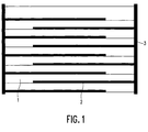
- the ceramic multilayer capacitor according to the invention comprises a ceramic dielectric 1 , which consists of a multiplicity of oxidic dielectric layers with a thickness of not more than 50 ⁇ , and a multiplicity of internal electrodes 2 , which are arranged one above the other in layers in the dielectric and alternate to form two opposing ones Extend end faces of the dielectric.
- metallic contact electrodes 3 are provided as external connections, which are connected to the corresponding inner metallic electrodes.
- the production takes place according to the usual manufacturing techniques for ceramic Capacitors, depending on the desired shape and dimensions, the desired accuracy and later use numerous manufacturing variants possible are.
- Material for the ceramic dielectric is a dielectric ceramic preparation with a doped barium calcium zirconium titanate with the composition (Ba 0.96 Ca 0.04 ) a [Ti 0.82-y Zr 0.18 Mn y ] O 3 with 0.001 ⁇ y ⁇ 0.01, 1,000 ⁇ a ⁇ 1.02 and that is doped with tungsten in an amount r of 0.001 to 0.005 mol / formula unit and yttrium in an amount s with 0.001 to 0.005 mol / formula unit.
- the dielectric ceramic preparation preferably contains SiO 2 as a sintering aid.
- the mixture can also contain 0.1-1% by weight of sintering aid consisting of 0.16 to 0.29 mol of lithium oxide, 0.004 to 0.39 mol of one of the oxides CaO, MgO, BaO or SrO and Silicon oxide, can be added. With this sintering aid, the sintering temperature can be reduced from 1300 o C to 1150 o C.
- the material selection for the electrodes is not subject to any particular restrictions, so that one uses a metal or a combination of two or more commonly used metals can use.
- the electrodes can be made Precious metals such as platinum, palladium, gold or silver exist. You can also Chromium, zirconium, vanadium, zinc, copper, tin, lead, manganese, molybdenum, Contain tungsten, titanium or aluminum. They preferably consist of a Base metal, selected from the group nickel, iron, cobalt and their Alloys.
- the production of the dielectric ceramic preparation can be carried out according to the usual Powder manufacturing methods, e.g. by the mixed oxide process, coprecipitation, Spray drying, sol / gel process, hdrothermal process or alkoxide process respectively.
- the mixed oxide process is preferred, in which the starting oxides or thermally decomposable compounds, e.g. Carbonates, hydroxides, Oxalates or acetates, mixed and ground. Then that will Starting powder calcined at 1000 ° C to 1400 ° C.
- a suspension is first produced from the calcined powder for shaping, which in addition to the powder as a further component solvent, binder and optionally contains plasticizers and dispersing agents.
- the solvent can be, for example, water, an alcohol, toluene, xylene or trichlorethylene.
- Organic polymers such as polyvinyl alcohol, Polyvinyl butyral or polymethymethacrylate is used.
- a plasticizer you can Use glycerin, polyglycols or phthalates. You can also use the suspension Dispersants such as alkylaryl polyether alcohols, polyethylene glycol ethyl ether or Add octylphenoxyethanol.
- Green ceramic films are produced from the suspension by the preferred method using a film casting process.
- the suspension is poured onto a moving carrier surface.
- a more or less flexible film remains, which is cut, printed with a metal paste in the pattern of the inner electrodes using the screen printing process and laminated.
- the individual multilayer capacitors are cut out of the laminate. These are first sintered in a weakly reducing atmosphere at temperatures between 1100 and 1400 o C and then annealed in a weakly oxidizing atmosphere at temperatures between 600 and 1100 o C. Nitrogen saturated with water vapor with an admixture of 0.5 to 2 vol.% Hydrogen can be used as the weakly reducing atmosphere, and nitrogen with 5 ppm to 100 ppm oxygen as the weakly oxidizing atmosphere.
- the outer electrodes are on the end faces of the capacitors a metal paste containing, for example, nickel, applied and baked.
- the outer electrodes can also be formed by evaporating a metal layer, for example made of gold.
- the sintered ceramic dielectric has a homogeneous microstructure Grain sizes below 5 ⁇ m.
- the dielectric constant ⁇ at 25 ° C. and the loss factor tg ⁇ were measured in a known manner.
- the service life ⁇ is measured in an accelerated service life test (ALT) at 350 o C and 900 V.
- ALT accelerated service life test
- test pills with a diameter of 5 mm and a layer thickness of 0.05 mm contacted with electrodes are produced, heated to 350 ° C. and a voltage of 1800 V / mm is applied.
- the current is measured, from which the insulation resistance is calculated.
- the insulation resistance is initially high.
- the insulation resistance remains essentially constant at a high level.
- the insulation resistance begins to drop only after a certain characteristic degradation time.
- the leakage current increases by several orders of magnitude in a short time compared to the previous measurement time.
- the lifetime ⁇ is defined as the time in which the leakage current has increased by an order of magnitude.
- Cyclohexane is used as grinding fluid and agate as grinding balls.
- the mixture is then ground for 24 h with 2mm YTZ balls in isopropanol.
- the mixture is dried in air under a surface evaporator and then calcined at 1250 ° C. for 6 hours.
- the powdery material is mixed with polyvinyl alcohol as a binder, a surface-active agent, a dispersant and water to form a slip.
- the slip is processed in a doctor blade coater to green ceramic films with a thickness of 20 microns.
- the green film is cut into film cards, printed with a nickel paste with the pattern of the inner electrodes, stacked and pressed together and separated into the individual capacitors.
- the capacitors are sintered at a temperature of 1300 o C.
- the heating rate is 300 ° C / h to 1000 ° C and 50 ° C / h to 1300 ° C.
- a gas mixture consisting of 99% N 2 and 1% H 2 is passed through the furnace, which is saturated with water vapor. It is cooled at 300 ° C / h.
- the capacitors are tempered in a tempering furnace at a temperature of 1000 ° C.
- a gas mixture consisting of nitrogen with 50 - 100 ppm oxygen is passed through the furnace.
- a 6 nm thick CrNi layer is evaporated as the outer electrodes 0.15 ⁇ m Au is coated.
- the powdery material is mixed with polyvinyl alcohol as a binder, a surface-active agent, a dispersant and water to form a suspension.
- the suspension is processed in a knife coater to green ceramic films with a thickness of 20 microns.
- the green film is cut into film cards, printed with a nickel paste with the pattern of the inner electrodes, stacked and pressed together and separated into the individual capacitors.
- the capacitors are sintered at a temperature of 1300 o C.
- the heating rate is 300 ° C / h to 1000 ° C and 50 ° C / h to 1300 ° C.
- a gas mixture consisting of 99% N 2 and 1% H 2 , which is saturated with water vapor, is passed through the furnace. It is cooled at 300 ° C./h.
- the capacitors are tempered in a tempering furnace at a temperature of 1000 ° C.
- a gas mixture consisting of nitrogen with 10-50 ppm oxygen is passed through the furnace.
- a 6 nm thick CrNi layer is evaporated as the outer electrodes 0.15 ⁇ m Au is coated.
- Cyclohexane is used as grinding fluid and agate as grinding balls.
- the mixture is then ground for 24 h with 2mm YTZ balls in isopropanol.
- the mixture is dried in air under a surface evaporator and then calcined at 1250 ° C. for 6 hours.
- the powdery material is mixed with polyvinyl alcohol as a binder, a surface-active agent, a dispersant and water to form a slip.
- the slip is processed in a doctor blade coater to green ceramic films with a thickness of 20 microns.
- the green film is cut into film cards, printed with a nickel paste with the pattern of the inner electrodes, stacked and pressed together and separated into the individual capacitors.
- the capacitors are sintered at a temperature of 1300 o C.
- the heating rate is 300 ° C / h to 1000 ° C and 50 ° C / h to 1300 ° C.
- a gas mixture consisting of 99% N 2 and 1% H 2 , which is saturated with water vapor, is passed through the furnace. It is cooled at 300 ° C./h.
- the capacitors are tempered in a tempering furnace at a temperature of 1000 ° C.
- a gas mixture consisting of nitrogen with 50 - 100 ppm oxygen is passed through the furnace.
- a 6 nm thick CrNi layer is evaporated as the outer electrodes 0.15 ⁇ m Au is coated.
- the mixture After grinding in the planetary ball mill, the mixture is dried in air under a surface evaporator and then calcined at 1250 ° C. for 6 hours.
- the powdery material is mixed with polyvinyl alcohol as a binder, a surface-active agent, a dispersant and water to form a slip.
- the slip is processed in a doctor blade coater to green ceramic films with a thickness of 20 microns.
- the green film is cut into film cards, printed with a nickel paste with the pattern of the inner electrodes, stacked and pressed together and separated into the individual capacitors.
- the capacitors are sintered at a temperature of 1300 o C.
- the heating rate is 300 ° C / h to 1000 ° C and 50 ° C / h to 1300 ° C.
- a gas mixture consisting of 99% N 2 and 1% H 2 , which is saturated with water vapor, is passed through the furnace. It is cooled at 300 ° C./h.
- the capacitors are tempered in a tempering furnace at a temperature of 1000 ° C.
- a gas mixture consisting of nitrogen with 50 - 100 ppm oxygen is passed through the furnace.
- a 6 nm thick CrNi layer is evaporated as the outer electrodes 0.15 ⁇ m Au is coated.
- Test results: ⁇ 13600; tan ⁇ ⁇ 5%, ⁇ > 150 h .
- the powdery material is mixed with polyvinyl alcohol as a binder, a surface-active agent, a dispersant and water to form a suspension.
- the suspension is processed in a knife coater to green ceramic films with a thickness of 20 microns.
- the green film is cut into film cards, printed with a nickel paste with the pattern of the inner electrodes, stacked and pressed together and separated into the individual capacitors.
- the capacitors are sintered at a temperature of 1300 o C.
- the heating rate is 300 ° C / h to 1000 ° C and 50 ° C / h to 1300 ° C.
- a gas mixture consisting of 99% N 2 and 1% H 2 , which is saturated with water vapor, is passed through the furnace. It is cooled at 300 ° C./h.
- the capacitors are tempered in a tempering furnace at a temperature of 1000 ° C.
- a gas mixture consisting of nitrogen with 10-50 ppm oxygen is passed through the furnace.
- a 6 nm thick CrNi layer is evaporated as the outer electrodes 0.15 ⁇ m Au is coated.
- Test results: ⁇ 15,800; tan ⁇ ⁇ 5%, ⁇ > 250 h .
- the powdery material is mixed with polyvinyl alcohol as a binder, a surface-active agent, a dispersant and water to form a suspension.
- the suspension is processed in a knife coater to green ceramic films with a thickness of 20 microns.
- the green film is cut into film cards, printed with a nickel paste with the pattern of the inner electrodes, stacked and pressed together and separated into the individual capacitors.
- the capacitors are sintered at a temperature of 1300 o C.
- the heating rate is 300 ° C / h to 1000 ° C and 50 ° C / h to 1300 ° C.
- a gas mixture consisting of 99% N 2 and 1% H 2 , which is saturated with water vapor, is passed through the furnace. It is cooled at 300 ° C./h.
- the capacitors are tempered in a tempering furnace at a temperature of 1000 ° C.
- a gas mixture consisting of nitrogen with 10-50 ppm oxygen is passed through the furnace.
- a 6 nm thick CrNi layer is evaporated as the outer electrodes 0.15 ⁇ m Au is coated.
Landscapes
- Engineering & Computer Science (AREA)
- Ceramic Engineering (AREA)
- Chemical & Material Sciences (AREA)
- Power Engineering (AREA)
- Inorganic Chemistry (AREA)
- Manufacturing & Machinery (AREA)
- Microelectronics & Electronic Packaging (AREA)
- Compositions Of Oxide Ceramics (AREA)
- Ceramic Capacitors (AREA)
Applications Claiming Priority (2)
| Application Number | Priority Date | Filing Date | Title |
|---|---|---|---|
| DE19635406A DE19635406B4 (de) | 1996-08-31 | 1996-08-31 | Kondensator und Vielschichtkondensator mit einem Dielektrium aus wolframhaltiger BCZT-Keramik |
| DE19635406 | 1996-08-31 |
Publications (1)
| Publication Number | Publication Date |
|---|---|
| EP0827166A1 true EP0827166A1 (de) | 1998-03-04 |
Family
ID=7804301
Family Applications (1)
| Application Number | Title | Priority Date | Filing Date |
|---|---|---|---|
| EP97202578A Withdrawn EP0827166A1 (de) | 1996-08-31 | 1997-08-21 | Vielschichtkondensator mit Wolfram-haltigem Batio3 |
Country Status (4)
| Country | Link |
|---|---|
| US (1) | US5889647A (enExample) |
| EP (1) | EP0827166A1 (enExample) |
| JP (1) | JPH1092685A (enExample) |
| DE (1) | DE19635406B4 (enExample) |
Cited By (4)
| Publication number | Priority date | Publication date | Assignee | Title |
|---|---|---|---|---|
| EP0899756A3 (de) * | 1997-08-28 | 2000-01-12 | Philips Patentverwaltung GmbH | Vielschichtkondensator mit silber- und seltenerdmetalldotiertem Bariumtitanat |
| WO2001033587A1 (de) * | 1999-10-29 | 2001-05-10 | Koninklijke Philips Electronics N.V. | Kondensator mit bczt-dielektrikum |
| EP1378922A4 (en) * | 2001-04-12 | 2007-09-12 | Tdk Corp | PROCESS FOR PRODUCING LAMINATED CERAMIC ELECTRONIC COMPONENT |
| CN118184348A (zh) * | 2024-04-07 | 2024-06-14 | 西安交通大学 | 一种兼具高储能密度和高储能效率的钛酸钡基陶瓷材料及其制备方法和用途 |
Families Citing this family (26)
| Publication number | Priority date | Publication date | Assignee | Title |
|---|---|---|---|---|
| JP3031268B2 (ja) * | 1996-11-20 | 2000-04-10 | 株式会社村田製作所 | 磁器コンデンサ |
| US6281142B1 (en) * | 1999-06-04 | 2001-08-28 | Micron Technology, Inc. | Dielectric cure for reducing oxygen vacancies |
| JP3506056B2 (ja) * | 1999-08-09 | 2004-03-15 | 株式会社村田製作所 | 正の抵抗温度特性を有する積層型半導体セラミック素子、および正の抵抗温度特性を有する積層型半導体セラミック素子の製造方法 |
| DE19939483A1 (de) * | 1999-08-20 | 2001-03-08 | Philips Corp Intellectual Pty | Passives Bauelement mit Verbundwerkstoff |
| US6337237B1 (en) * | 1999-09-01 | 2002-01-08 | Micron Technology, Inc. | Capacitor processing method and DRAM processing method |
| JP3361091B2 (ja) * | 2000-06-20 | 2003-01-07 | ティーディーケイ株式会社 | 誘電体磁器および電子部品 |
| US7914755B2 (en) * | 2001-04-12 | 2011-03-29 | Eestor, Inc. | Method of preparing ceramic powders using chelate precursors |
| JP4446324B2 (ja) * | 2001-09-27 | 2010-04-07 | 株式会社村田製作所 | 誘電体磁器組成物及びそれを用いたコンデンサ |
| KR100466072B1 (ko) * | 2002-05-24 | 2005-01-13 | 삼성전기주식회사 | 적층 세라믹 콘덴서용 유전체 조성물 및 이를 이용한 적층세라믹 콘덴서 |
| KR100506731B1 (ko) * | 2002-12-24 | 2005-08-08 | 삼성전기주식회사 | 저온 소성 유전체 조성물, 적층 세라믹 커패시터 및세라믹 전자부품 |
| JP2005057174A (ja) * | 2003-08-07 | 2005-03-03 | Matsushita Electric Ind Co Ltd | セラミック電子部品の製造方法 |
| US7218504B2 (en) * | 2004-03-02 | 2007-05-15 | Intel Corporation | Capacitor device and method |
| US20060000542A1 (en) * | 2004-06-30 | 2006-01-05 | Yongki Min | Metal oxide ceramic thin film on base metal electrode |
| US7290315B2 (en) * | 2004-10-21 | 2007-11-06 | Intel Corporation | Method for making a passive device structure |
| US20060099803A1 (en) * | 2004-10-26 | 2006-05-11 | Yongki Min | Thin film capacitor |
| US20060091495A1 (en) * | 2004-10-29 | 2006-05-04 | Palanduz Cengiz A | Ceramic thin film on base metal electrode |
| US7375412B1 (en) * | 2005-03-31 | 2008-05-20 | Intel Corporation | iTFC with optimized C(T) |
| US7629269B2 (en) * | 2005-03-31 | 2009-12-08 | Intel Corporation | High-k thin film grain size control |
| US20060220177A1 (en) * | 2005-03-31 | 2006-10-05 | Palanduz Cengiz A | Reduced porosity high-k thin film mixed grains for thin film capacitor applications |
| US7453144B2 (en) * | 2005-06-29 | 2008-11-18 | Intel Corporation | Thin film capacitors and methods of making the same |
| US8623737B2 (en) * | 2006-03-31 | 2014-01-07 | Intel Corporation | Sol-gel and mask patterning for thin-film capacitor fabrication, thin-film capacitors fabricated thereby, and systems containing same |
| US7993611B2 (en) | 2006-08-02 | 2011-08-09 | Eestor, Inc. | Method of preparing ceramic powders using ammonium oxalate |
| US8853116B2 (en) | 2006-08-02 | 2014-10-07 | Eestor, Inc. | Method of preparing ceramic powders |
| WO2010089241A1 (de) | 2009-02-04 | 2010-08-12 | Basf Se | Schwarze, uv-stabile thermoplastische formmassen |
| US7987566B2 (en) * | 2009-07-15 | 2011-08-02 | Sturzebecher Richard J | Capacitor forming method |
| KR102762893B1 (ko) * | 2018-12-12 | 2025-02-07 | 삼성전기주식회사 | 적층 세라믹 전자부품 |
Citations (1)
| Publication number | Priority date | Publication date | Assignee | Title |
|---|---|---|---|---|
| US5319517A (en) * | 1992-03-27 | 1994-06-07 | Tdk Corporation | Multilayer ceramic chip capacitor |
Family Cites Families (7)
| Publication number | Priority date | Publication date | Assignee | Title |
|---|---|---|---|---|
| JPS61250905A (ja) * | 1985-04-26 | 1986-11-08 | ティーディーケイ株式会社 | 誘電体磁器組成物及びその製造法 |
| MX172902B (es) * | 1986-05-05 | 1994-01-20 | Cabot Corp | Coformas de titanato de bario |
| DE3723082C2 (de) * | 1986-07-14 | 2003-09-25 | Cabot Corp | Verfahren zur Herstellung von submikronen Perovskiten |
| ES2006956A6 (es) * | 1987-08-12 | 1989-05-16 | Cabot Corp | Coformas de titanato de bario dopado. |
| JP2529410B2 (ja) * | 1989-09-25 | 1996-08-28 | 松下電器産業株式会社 | 誘電体磁器組成物とそれを用いた積層セラミックコンデンサとその製造方法 |
| JPH0779004B2 (ja) * | 1990-10-31 | 1995-08-23 | 株式会社村田製作所 | 誘電体磁器組成物 |
| JP2952062B2 (ja) * | 1991-02-18 | 1999-09-20 | ティーディーケイ株式会社 | 非還元性誘電体磁器組成物 |
-
1996
- 1996-08-31 DE DE19635406A patent/DE19635406B4/de not_active Expired - Fee Related
-
1997
- 1997-08-21 EP EP97202578A patent/EP0827166A1/de not_active Withdrawn
- 1997-08-26 US US08/918,847 patent/US5889647A/en not_active Expired - Fee Related
- 1997-08-28 JP JP9231920A patent/JPH1092685A/ja active Pending
Patent Citations (1)
| Publication number | Priority date | Publication date | Assignee | Title |
|---|---|---|---|---|
| US5319517A (en) * | 1992-03-27 | 1994-06-07 | Tdk Corporation | Multilayer ceramic chip capacitor |
Cited By (4)
| Publication number | Priority date | Publication date | Assignee | Title |
|---|---|---|---|---|
| EP0899756A3 (de) * | 1997-08-28 | 2000-01-12 | Philips Patentverwaltung GmbH | Vielschichtkondensator mit silber- und seltenerdmetalldotiertem Bariumtitanat |
| WO2001033587A1 (de) * | 1999-10-29 | 2001-05-10 | Koninklijke Philips Electronics N.V. | Kondensator mit bczt-dielektrikum |
| EP1378922A4 (en) * | 2001-04-12 | 2007-09-12 | Tdk Corp | PROCESS FOR PRODUCING LAMINATED CERAMIC ELECTRONIC COMPONENT |
| CN118184348A (zh) * | 2024-04-07 | 2024-06-14 | 西安交通大学 | 一种兼具高储能密度和高储能效率的钛酸钡基陶瓷材料及其制备方法和用途 |
Also Published As
| Publication number | Publication date |
|---|---|
| JPH1092685A (ja) | 1998-04-10 |
| DE19635406B4 (de) | 2005-09-01 |
| DE19635406A1 (de) | 1998-03-05 |
| US5889647A (en) | 1999-03-30 |
Similar Documents
| Publication | Publication Date | Title |
|---|---|---|
| EP0899756B1 (de) | Vielschichtkondensator mit silber- oder seltenerdmetalldotiertem Barium-Calcium-Zirkon-Titanat | |
| DE19635406B4 (de) | Kondensator und Vielschichtkondensator mit einem Dielektrium aus wolframhaltiger BCZT-Keramik | |
| DE60014225T2 (de) | Keramischer Vielschichtkondensator mit hoher Zuverlässigkeit, kompatibel mit Nickelelektroden | |
| EP0782156A2 (de) | Vielschichtkondensator mit Dielektrikum aus modifiziertem Bariumstrontiumtitanat | |
| DE69728721T2 (de) | Dielektrische keramische Zusammensetzung und dieselbe benutzender monolithischer keramischer Kondensator | |
| DE69034034T2 (de) | Keramischer Mehrschicht-Chipkondensator und Verfahren zu seiner Herstellung | |
| DE69516045T2 (de) | Keramischer Mehrschichtkondensator und Herstellungsverfahren | |
| DE69700235T2 (de) | Monolithischer keramischer Kondensator | |
| US7061748B2 (en) | Multilayer ceramic capacitor | |
| DE69710259T2 (de) | Dielektrische keramische Zusammensetzung und ihre Verwendung in einem monolithischen keramischen Kondensator | |
| DE10126099B4 (de) | Keramischer Vielschichtkondensator und Verfahren zu seiner Herstellung | |
| DE69619947T2 (de) | Dielektrische keramische Zusammensetzung und ihre Verwendung für einen monolithischen Kondensator | |
| DE102012109362B4 (de) | Dielektrische Zusammensetzung und diese enthaltendes keramisches Elektronikbauteil | |
| DE69632659T2 (de) | Vielschichtvaristor | |
| DE69209417T2 (de) | Nichtreduzierbare dielektrische keramische Zusammensetzung | |
| EP1612817B1 (en) | Multilayer ceramic capacitor | |
| DE69604510T2 (de) | Monolithische keramische Kondensatoren | |
| DE10121503A1 (de) | Dielektrische Keramik und elektronisches Bauteil mit einer solchen | |
| JPH1092685A5 (enExample) | ||
| DE60129533T2 (de) | Dielektrische porzellan zusammensetzung und elektronische teile | |
| EP1145261A1 (de) | Kondensator mit bczt-dielektrikum | |
| US8320103B2 (en) | Dielectric ceramic and laminated ceramic capacitor | |
| DE69400553T2 (de) | Nicht-reduzierbare dielektrische keramische Zusammensetzung | |
| DE69513179T2 (de) | Hochtemperaturstabiler dielektrischer Werkstoff | |
| DE60126918T2 (de) | Dielektrische Keramikkomposition, Verfahren zur Herstellung eines Keramikkondensators, Verwendung eines keramischen Dielektrikums, und Keramikkondensator |
Legal Events
| Date | Code | Title | Description |
|---|---|---|---|
| PUAI | Public reference made under article 153(3) epc to a published international application that has entered the european phase |
Free format text: ORIGINAL CODE: 0009012 |
|
| AK | Designated contracting states |
Kind code of ref document: A1 Designated state(s): DE FR GB |
|
| AX | Request for extension of the european patent |
Free format text: AL;LT;LV;RO;SI |
|
| RAP3 | Party data changed (applicant data changed or rights of an application transferred) |
Owner name: KONINKLIJKE PHILIPS ELECTRONICS N.V. Owner name: PHILIPS PATENTVERWALTUNG GMBH |
|
| 17P | Request for examination filed |
Effective date: 19980904 |
|
| AKX | Designation fees paid |
Free format text: DE FR GB |
|
| RBV | Designated contracting states (corrected) |
Designated state(s): DE FR GB |
|
| STAA | Information on the status of an ep patent application or granted ep patent |
Free format text: STATUS: THE APPLICATION HAS BEEN WITHDRAWN |
|
| 18W | Application withdrawn |
Withdrawal date: 19990531 |