EP0825638A2 - Verfahren zur Herstellung feiner Strukturen - Google Patents
Verfahren zur Herstellung feiner Strukturen Download PDFInfo
- Publication number
- EP0825638A2 EP0825638A2 EP97110326A EP97110326A EP0825638A2 EP 0825638 A2 EP0825638 A2 EP 0825638A2 EP 97110326 A EP97110326 A EP 97110326A EP 97110326 A EP97110326 A EP 97110326A EP 0825638 A2 EP0825638 A2 EP 0825638A2
- Authority
- EP
- European Patent Office
- Prior art keywords
- nuclei
- layer
- dielectric layer
- mask
- substrate
- Prior art date
- Legal status (The legal status is an assumption and is not a legal conclusion. Google has not performed a legal analysis and makes no representation as to the accuracy of the status listed.)
- Granted
Links
Images
Classifications
-
- H—ELECTRICITY
- H10—SEMICONDUCTOR DEVICES; ELECTRIC SOLID-STATE DEVICES NOT OTHERWISE PROVIDED FOR
- H10P—GENERIC PROCESSES OR APPARATUS FOR THE MANUFACTURE OR TREATMENT OF DEVICES COVERED BY CLASS H10
- H10P14/00—Formation of materials, e.g. in the shape of layers or pillars
- H10P14/20—Formation of materials, e.g. in the shape of layers or pillars of semiconductor materials
- H10P14/27—Formation of materials, e.g. in the shape of layers or pillars of semiconductor materials using selective deposition, e.g. simultaneous growth of monocrystalline and non-monocrystalline semiconductor materials
- H10P14/271—Formation of materials, e.g. in the shape of layers or pillars of semiconductor materials using selective deposition, e.g. simultaneous growth of monocrystalline and non-monocrystalline semiconductor materials characterised by the preparation of substrate for selective deposition
-
- B—PERFORMING OPERATIONS; TRANSPORTING
- B82—NANOTECHNOLOGY
- B82Y—SPECIFIC USES OR APPLICATIONS OF NANOSTRUCTURES; MEASUREMENT OR ANALYSIS OF NANOSTRUCTURES; MANUFACTURE OR TREATMENT OF NANOSTRUCTURES
- B82Y10/00—Nanotechnology for information processing, storage or transmission, e.g. quantum computing or single electron logic
-
- C—CHEMISTRY; METALLURGY
- C23—COATING METALLIC MATERIAL; COATING MATERIAL WITH METALLIC MATERIAL; CHEMICAL SURFACE TREATMENT; DIFFUSION TREATMENT OF METALLIC MATERIAL; COATING BY VACUUM EVAPORATION, BY SPUTTERING, BY ION IMPLANTATION OR BY CHEMICAL VAPOUR DEPOSITION, IN GENERAL; INHIBITING CORROSION OF METALLIC MATERIAL OR INCRUSTATION IN GENERAL
- C23C—COATING METALLIC MATERIAL; COATING MATERIAL WITH METALLIC MATERIAL; SURFACE TREATMENT OF METALLIC MATERIAL BY DIFFUSION INTO THE SURFACE, BY CHEMICAL CONVERSION OR SUBSTITUTION; COATING BY VACUUM EVAPORATION, BY SPUTTERING, BY ION IMPLANTATION OR BY CHEMICAL VAPOUR DEPOSITION, IN GENERAL
- C23C16/00—Chemical coating by decomposition of gaseous compounds, without leaving reaction products of surface material in the coating, i.e. chemical vapour deposition [CVD] processes
- C23C16/04—Coating on selected surface areas, e.g. using masks
-
- H—ELECTRICITY
- H10—SEMICONDUCTOR DEVICES; ELECTRIC SOLID-STATE DEVICES NOT OTHERWISE PROVIDED FOR
- H10B—ELECTRONIC MEMORY DEVICES
- H10B41/00—Electrically erasable-and-programmable ROM [EEPROM] devices comprising floating gates
-
- H—ELECTRICITY
- H10—SEMICONDUCTOR DEVICES; ELECTRIC SOLID-STATE DEVICES NOT OTHERWISE PROVIDED FOR
- H10D—INORGANIC ELECTRIC SEMICONDUCTOR DEVICES
- H10D30/00—Field-effect transistors [FET]
- H10D30/01—Manufacture or treatment
- H10D30/021—Manufacture or treatment of FETs having insulated gates [IGFET]
- H10D30/0411—Manufacture or treatment of FETs having insulated gates [IGFET] of FETs having floating gates
-
- H—ELECTRICITY
- H10—SEMICONDUCTOR DEVICES; ELECTRIC SOLID-STATE DEVICES NOT OTHERWISE PROVIDED FOR
- H10D—INORGANIC ELECTRIC SEMICONDUCTOR DEVICES
- H10D64/00—Electrodes of devices having potential barriers
- H10D64/01—Manufacture or treatment
- H10D64/031—Manufacture or treatment of data-storage electrodes
- H10D64/035—Manufacture or treatment of data-storage electrodes comprising conductor-insulator-conductor-insulator-semiconductor structures
-
- H—ELECTRICITY
- H10—SEMICONDUCTOR DEVICES; ELECTRIC SOLID-STATE DEVICES NOT OTHERWISE PROVIDED FOR
- H10P—GENERIC PROCESSES OR APPARATUS FOR THE MANUFACTURE OR TREATMENT OF DEVICES COVERED BY CLASS H10
- H10P14/00—Formation of materials, e.g. in the shape of layers or pillars
- H10P14/20—Formation of materials, e.g. in the shape of layers or pillars of semiconductor materials
- H10P14/24—Formation of materials, e.g. in the shape of layers or pillars of semiconductor materials using chemical vapour deposition [CVD]
-
- H—ELECTRICITY
- H10—SEMICONDUCTOR DEVICES; ELECTRIC SOLID-STATE DEVICES NOT OTHERWISE PROVIDED FOR
- H10P—GENERIC PROCESSES OR APPARATUS FOR THE MANUFACTURE OR TREATMENT OF DEVICES COVERED BY CLASS H10
- H10P14/00—Formation of materials, e.g. in the shape of layers or pillars
- H10P14/20—Formation of materials, e.g. in the shape of layers or pillars of semiconductor materials
- H10P14/29—Formation of materials, e.g. in the shape of layers or pillars of semiconductor materials characterised by the substrates
- H10P14/2901—Materials
- H10P14/2902—Materials being Group IVA materials
- H10P14/2905—Silicon, silicon germanium or germanium
-
- H—ELECTRICITY
- H10—SEMICONDUCTOR DEVICES; ELECTRIC SOLID-STATE DEVICES NOT OTHERWISE PROVIDED FOR
- H10P—GENERIC PROCESSES OR APPARATUS FOR THE MANUFACTURE OR TREATMENT OF DEVICES COVERED BY CLASS H10
- H10P14/00—Formation of materials, e.g. in the shape of layers or pillars
- H10P14/20—Formation of materials, e.g. in the shape of layers or pillars of semiconductor materials
- H10P14/29—Formation of materials, e.g. in the shape of layers or pillars of semiconductor materials characterised by the substrates
- H10P14/2901—Materials
- H10P14/2923—Materials being conductive materials, e.g. metallic silicides
-
- H—ELECTRICITY
- H10—SEMICONDUCTOR DEVICES; ELECTRIC SOLID-STATE DEVICES NOT OTHERWISE PROVIDED FOR
- H10P—GENERIC PROCESSES OR APPARATUS FOR THE MANUFACTURE OR TREATMENT OF DEVICES COVERED BY CLASS H10
- H10P14/00—Formation of materials, e.g. in the shape of layers or pillars
- H10P14/20—Formation of materials, e.g. in the shape of layers or pillars of semiconductor materials
- H10P14/34—Deposited materials, e.g. layers
- H10P14/3402—Deposited materials, e.g. layers characterised by the chemical composition
- H10P14/3404—Deposited materials, e.g. layers characterised by the chemical composition being Group IVA materials
- H10P14/3411—Silicon, silicon germanium or germanium
-
- H—ELECTRICITY
- H10—SEMICONDUCTOR DEVICES; ELECTRIC SOLID-STATE DEVICES NOT OTHERWISE PROVIDED FOR
- H10P—GENERIC PROCESSES OR APPARATUS FOR THE MANUFACTURE OR TREATMENT OF DEVICES COVERED BY CLASS H10
- H10P76/00—Manufacture or treatment of masks on semiconductor bodies, e.g. by lithography or photolithography
- H10P76/40—Manufacture or treatment of masks on semiconductor bodies, e.g. by lithography or photolithography of masks comprising inorganic materials
- H10P76/408—Manufacture or treatment of masks on semiconductor bodies, e.g. by lithography or photolithography of masks comprising inorganic materials characterised by their sizes, orientations, dispositions, behaviours or shapes
Definitions
- etching masks In view of the increasing miniaturization in the Semiconductor technology Masks with increasingly fine structures needed.
- the masks are called etching masks or implantation masks used.
- Such a device which is suitable as a volatile and non-volatile memory, is, for. B. in S. Tiwari et al, IEDM 95, pp. 521-524.
- the component comprises a MOS transistor, in the gate dielectric of which so-called silicon nano-crystals are provided as charge stores. These are small silicon crystals with a diameter of 5 nm, which are embedded in a matrix of SiO 2 . Charge is stored in these silicon crystals and, like the charge stored on a floating gate of an EEPROM, influences the threshold voltage of the MOS transistor. SiO 2 arranged below the silicon crystals acts as a tunnel oxide. The silicon crystals are formed by spontaneous decomposition and combination of material during CVD deposition. The size and packing density of the resulting silicon crystals are difficult to control.
- the invention is therefore based on the problem of a method to specify fine structures at which the packing density the fine structures are more adjustable.
- the size of the fine structures should be adjustable be.
- nuclei are formed on the surface of a substrate in a CVD process using a first process gas, which contains SiH 4 and GeH 4 in a carrier gas, which determine the dimensions of the fine structures.
- a first process gas which contains SiH 4 and GeH 4 in a carrier gas, which determine the dimensions of the fine structures.
- Such germs are also called nanocrystals. The germs emerge statistically distributed without the use of lithographic processes. Therefore, smaller structure sizes can be achieved than corresponds to the resolution of the lithography.
- the nucleation is interrupted as soon as a predetermined density of the germs is reached.
- the size of the nuclei is then adjusted by selective epitaxy of silicon.
- a second process gas is used, which contains SiH 2 CL 2 in a carrier gas, e.g. H 2.
- the selective epitaxy takes place in the temperature range between 600 ° C and 800 ° C.
- This gas mixture can also GeH 4 added to the material composition of the germs and thus material properties such.
- the nuclei are preferably formed with structure sizes in the range between 1 and 100 nm. This means that the diameters of the nuclei are in the range between 1 and 100 nm and the distances between neighboring statistically distributed mask structures are also in this size range. Packing densities in the range between 10 8 and 10 13 per cm 2 are thus achieved.
- the substrate Mask layer includes.
- the germs are on their surface educated. By anisotropic etching using the germs the mask layer then becomes an etching mask Mask formed.
- the mask can be used as an etching mask as well can be used as an implantation mask or the like. she has structures in the size of the germs.
- a substrate to apply the first dielectric layer on the surface thereof the germs are formed. Then there is a second dielectric layer and a conductive layer applied.
- the conductive layer, the first dielectric The layer and the second dielectric layer are structured. This involves a gate electrode and a gate dielectric of a MOS transistor. In the gate dielectric form the between the first dielectric layer and the second dielectric layer arranged nuclei charge storage. A source region and a drain region are formed in the substrate formed for the MOS transistor.
- the nuclei are preferably made of silicon / germanium educated.
- the work function is above the germanium portion in the germs adjustable. This is a work function engineering possible.
- a substrate z. B a semiconductor substrate, preferably made of monocrystalline silicon or an SOI substrate, the surface of which is provided with an insulating layer is.
- a layer 2 to be structured On a substrate 1 from z. B. monocrystalline silicon is a layer 2 to be structured from z. B. polysilicon, epitaxially grown silicon, metal, metal silicide, SiO 2 , Si 3 N 4 or the like.
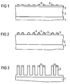
- a mask layer 3 is arranged thereon from a material which is suitable as an etching mask when structuring the layer 2 to be structured. If the layer 2 to be structured is made of silicon, then for the mask layer 3 z. B. SiO 2 suitable (see FIG. 1).
- Statistically distributed nuclei 4 are formed on the surface of the mask layer 3 during a gas phase deposition in an epitaxial system.
- An atmosphere of H 2 and SiH 4 is used as the process gas, H 2 forming the carrier gas.
- the atmosphere also includes GeH 4 added to delay the nucleation process.
- the partial pressure of SiH 4 and GeH 4 is in the range from 10 -3 to 1 mbar, the partial pressure of H 2 is in the range from 1 to 100 mbar.
- the deposition is carried out in the temperature range between 500 ° C and 700 ° C. Under these process conditions, 3 individual nuclei 4 made of silicon form on the surface of the mask layer. As soon as the density of the nuclei 4 has reached a predetermined density of approximately 10 10 / cm 2 , the nucleation process is stopped.
- the process conditions are then changed in order to selectively set the size of the germs 4.
- process conditions are set as they are used for the selective epitaxy. Under these process conditions, further nucleation on the surface of the mask layer 3 is prevented.
- the selective epitaxy takes place e.g. B. with a gas mixture of H 2 and SiH 2 Cl 2 in the temperature range between 600 ° C and 800 ° C.
- GeH 4 can also be added to this gas mixture in order to determine the material composition of the nuclei 4 and thus material properties such as. B. etching selectivities and the like.
- the deposition process is terminated.
- the germs 4 form a statistical mask.
- the mask layer 3 selectively attacks the germs 4, the mask layer 3 structured.
- the mask layer 3 becomes a mask 5 formed (see Figure 2).
- An anisotropic etching process is then carried out, which selectively attacks silicon to SiO 2 .
- the layer 2 to be structured is structured (see FIG. 3).
- the germs 4, which consist of silicon or silicon germanium, are removed.
- the anisotropic etching process is e.g. B. performed with HBr.
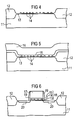
- Field oxide regions 12 formed an active area for define a MOS transistor (see FIG. 4).
- a first dielectric layer 13 made of e.g. B. SiO 2 in a layer thickness of z. B. 3 nm formed.
- Statistically distributed nuclei 14 are formed on the surface of the first dielectric layer 13 during a gas phase deposition in an epitaxial system.
- An atmosphere of H 2 and SiH 4 is used as the process gas, H 2 forming the carrier gas.
- the atmosphere also includes GeH 4 added to delay the nucleation process.
- the partial pressure of SiH 4 GeH 4 is in the range from 10 -3 to 1 mbar, the partial pressure of H 2 is in the range from 1 to 100 mbar.
- the deposition is carried out in the temperature range between 500 ° C and 700 ° C. Under these process conditions, individual nuclei 14 made of silicon are formed on the surface of the first dielectric layer 13. As soon as the density of the nuclei 14 has reached a predetermined density of approximately 10 8 / cm 2 , the nucleation process is stopped.
- the process conditions are then changed in order to selectively set the size of the germs 14.
- process conditions are set as they are used for the selective epitaxy. Under these process conditions, further nucleation on the surface of the first / dielectric layer 13 is prevented.
- the selective epitaxy takes place e.g. B. with a gas mixture of H 2 and SiH 2 Cl 2 in the temperature range between 600 ° C and 800 ° C. GeH 4 will also be added to this gas mixture in order to adjust the material composition of the nuclei 4 and thus the exit energy.
- the nuclei are formed with a diameter of, for example, 5 nm and a surface density of, for example, 10 12 cm -2 .
- the nuclei 14 form charge stores in the MOS transistor.
- the conductive layer 16 is z. B. 150 nm formed.
- the gate dielectric 18 comprises the structured first dielectric layer 13 and the structured second dielectric layer 15 as well the nuclei arranged in between. Outside the gate dielectric 18 seeds 14 arranged during the structuring also removed.
- spacers 19 of SiO 2 are formed on the flanks of the gate electrode 17 and gate dielectric 18.
- z. B. of phosphorus or Arsenic self-aligned to the gate electrode 17 and to the field oxide areas 12 source / drain regions 19 are formed.
- the MOS transistor As volatile or non-volatile memory suitable.
- the information is in the form of in the germs 14 captured charge stored.
Landscapes
- Chemical & Material Sciences (AREA)
- Engineering & Computer Science (AREA)
- Nanotechnology (AREA)
- Materials Engineering (AREA)
- Theoretical Computer Science (AREA)
- Mechanical Engineering (AREA)
- Metallurgy (AREA)
- Organic Chemistry (AREA)
- Physics & Mathematics (AREA)
- Mathematical Physics (AREA)
- Chemical Kinetics & Catalysis (AREA)
- Crystallography & Structural Chemistry (AREA)
- General Chemical & Material Sciences (AREA)
- Semiconductor Memories (AREA)
- Insulated Gate Type Field-Effect Transistor (AREA)
- Non-Volatile Memory (AREA)
- Drying Of Semiconductors (AREA)
- Chemical Vapour Deposition (AREA)
Abstract
Description
- Figur 1
- zeigt ein Substrat mit einer zu strukturierenden Schicht und einer Maskenschicht nach der Bildung von Keimen auf der Oberfläche der Maskenschicht.
- Figur 2
- zeigt das Substrat nach Strukturierung der Maskenschicht unter Verwendung der Keime als Ätzmaske.
- Figur 3
- zeigt das Substrat nach Verwendung der strukturierten Maskenschicht als Ätzmaske bei der Strukturierung der zu strukturierenden Schicht.
- Figur 4
- zeigt ein Substrat mit Feldoxidbereichen, einer ersten dielektrischen Schicht und auf der Oberfläche der ersten dielektrischen Schicht gebildeten Keimen.
- Figur 5
- zeigt das Substrat nach Aufbringen einer zweiten dielektrischen Schicht und einer leitfähigen Schicht.
- Figur 6
- zeigt das Substrat nach Bildung einer Gateelektrode und eines Gatedielektrikums sowie von Source- und Drain-Gebieten.
- 1
- Substrat
- 2
- zu strukturierende Schicht
- 3
- Maskenschicht
- 4
- Keime
- 5
- Maske
- 11
- Substrat
- 12
- Feldoxidbereiche
- 13
- erste dielektrische Schicht
- 14
- Keime
- 15
- zweite dielektrische Schicht
- 16
- leitfähige Schicht
- 17
- Gateelektrode
- 18
- Gatedielektrikum
- 19
- Spacer
- 20
- Source-/Drain-Gebiete
Claims (5)
- Verfahren zur Herstellung feiner Strukturen,bei dem auf der Oberfläche eines Substrats (1, 2, 3) in einem CVD-Verfahren unter Verwendung eines ersten Prozeßgases, das in einem Trägergas SiH4 und GeH4 enthält, Keime (4) gebildet werden, die die Abmessungen der feinen Strukturen bestimmen,bei dem das CVD-Verfahren unter Verwendung des ersten Prozeßgases unterbrochen wird, sobald die Keime (4) eine vorgegebene Dichte erreicht haben,bei dem durch selektive Epitaxie unter Verwendung eines zweiten Prozeßgases, das SiCl2H2 und/oder GeH4 in einem Trägergas enthält, die Größe der Keime (4) eingestellt wird.
- Verfahren nach Anspruch 1,
bei dem das erste Prozeßgas als Trägergas H2, N2, AR, oder He enthält. - Verfahren nach Anspruch 1 oder 2,
bei dem die Keime (4) mittlere Durchmesser und mittlere Abstände jeweils im Bereich zwischen 1 und 100 nm aufweisen. - Verfahren nach einem der Ansprüche 1 bis 3,bei dem das Substrat eine Maskenschicht (3) umfaßt, auf deren Oberfläche die Keime (4) gebildet werden,bei dem durch anisotropes Ätzen unter Verwendung der Keime als Ätzmaske aus der Maskenschicht (3) eine Maske (5) gebildet wird.
- Verfahren nach einem der Ansprüche 1 bis 3,bei dem auf das Substrat (11) eine erste dielektrische Schicht (13) aufgebracht wird, auf deren Oberfläche die Keime (14) gebildet werden,bei dem eine zweite dielektrische Schicht (15) und eine leitfähige Schicht (16) aufgebracht werden,bei dem die leitfähige Schicht (16) und die erste dielektrische Schicht (13) und die zweite dielektrische Schicht (15) strukturiert werden zur Bildung einer Gateelektrode (17) und eines Gatedielektrikums (18) eines MOS-Transistors, in dem die zwischen der ersten dielektrischen Schicht (13) und der zweiten dielektrischen Schicht (15) angeordneten Keime (14) Ladungsspeicher bilden,bei dem im Substrat (11) ein Source-Gebiet und ein Drain-Gebiet (20) für den MOS-Transistor gebildet werden.
Applications Claiming Priority (2)
| Application Number | Priority Date | Filing Date | Title |
|---|---|---|---|
| DE19632834A DE19632834C2 (de) | 1996-08-14 | 1996-08-14 | Verfahren zur Herstellung feiner Strukturen und dessen Verwendung zur Herstellung einer Maske und eines MOS-Transistors |
| DE19632834 | 1996-08-14 |
Publications (3)
| Publication Number | Publication Date |
|---|---|
| EP0825638A2 true EP0825638A2 (de) | 1998-02-25 |
| EP0825638A3 EP0825638A3 (de) | 1998-12-23 |
| EP0825638B1 EP0825638B1 (de) | 2001-10-04 |
Family
ID=7802658
Family Applications (1)
| Application Number | Title | Priority Date | Filing Date |
|---|---|---|---|
| EP97110326A Expired - Lifetime EP0825638B1 (de) | 1996-08-14 | 1997-06-24 | Verfahren zur Herstellung feiner Strukturen |
Country Status (6)
| Country | Link |
|---|---|
| US (1) | US5943571A (de) |
| EP (1) | EP0825638B1 (de) |
| JP (1) | JPH10112440A (de) |
| KR (1) | KR19980018652A (de) |
| DE (2) | DE19632834C2 (de) |
| TW (1) | TW350093B (de) |
Families Citing this family (19)
| Publication number | Priority date | Publication date | Assignee | Title |
|---|---|---|---|---|
| JP4538693B2 (ja) * | 1998-01-26 | 2010-09-08 | ソニー株式会社 | メモリ素子およびその製造方法 |
| KR100271211B1 (ko) * | 1998-07-15 | 2000-12-01 | 윤덕용 | 나노결정을 이용한 비휘발성 기억소자 형성방법 |
| JP2000106401A (ja) * | 1998-09-29 | 2000-04-11 | Sony Corp | メモリ素子およびその製造方法ならびに集積回路 |
| JP3368225B2 (ja) | 1999-03-11 | 2003-01-20 | キヤノン株式会社 | 回折光学素子の製造方法 |
| TW429607B (en) * | 1999-04-13 | 2001-04-11 | United Microelectronics Corp | Structure of dynamic random access memory capacitor and its fabricating method |
| DE10034005A1 (de) * | 2000-07-07 | 2002-01-24 | Infineon Technologies Ag | Verfahren zum Erzeugen von Mikro-Rauhigkeiten auf einer Oberfläche |
| US6455372B1 (en) * | 2000-08-14 | 2002-09-24 | Micron Technology, Inc. | Nucleation for improved flash erase characteristics |
| KR100425934B1 (ko) * | 2000-12-29 | 2004-04-03 | 주식회사 하이닉스반도체 | 실리콘-게르마늄막 형성 방법 |
| US7136441B2 (en) * | 2001-01-24 | 2006-11-14 | Matsushita Electric Industrial Co., Ltd. | Clock recovery circuit |
| US7145704B1 (en) | 2003-11-25 | 2006-12-05 | Cheetah Omni, Llc | Optical logic gate based optical router |
| US6656792B2 (en) * | 2001-10-19 | 2003-12-02 | Chartered Semiconductor Manufacturing Ltd | Nanocrystal flash memory device and manufacturing method therefor |
| KR100526463B1 (ko) * | 2003-05-07 | 2005-11-08 | 매그나칩 반도체 유한회사 | 반도체 소자의 제조 방법 |
| US7170666B2 (en) * | 2004-07-27 | 2007-01-30 | Hewlett-Packard Development Company, L.P. | Nanostructure antireflection surfaces |
| US7160775B2 (en) * | 2004-08-06 | 2007-01-09 | Freescale Semiconductor, Inc. | Method of discharging a semiconductor device |
| JP4739729B2 (ja) * | 2004-11-08 | 2011-08-03 | パナソニック株式会社 | 反射防止構造体を備えた部材の製造方法 |
| US7186616B2 (en) * | 2005-03-16 | 2007-03-06 | Freescale Semiconductor, Inc. | Method of removing nanoclusters in a semiconductor device |
| US8067803B2 (en) | 2008-10-16 | 2011-11-29 | Micron Technology, Inc. | Memory devices, transistor devices and related methods |
| US9773889B2 (en) * | 2014-07-18 | 2017-09-26 | Taiwan Semiconductor Manufacturing Company Limited | Method of semiconductor arrangement formation |
| CN111293118B (zh) * | 2018-12-10 | 2023-07-04 | 中芯国际集成电路制造(上海)有限公司 | 半导体结构及其形成方法 |
Family Cites Families (11)
| Publication number | Priority date | Publication date | Assignee | Title |
|---|---|---|---|---|
| US4698316A (en) * | 1985-01-23 | 1987-10-06 | Rca Corporation | Method of depositing uniformly thick selective epitaxial silicon |
| KR930009583B1 (ko) * | 1990-11-29 | 1993-10-07 | 삼성전자 주식회사 | 융모모양의 커패시터구조를 가진 반도체 메모리장치의 제조방법 |
| JPH0521798A (ja) * | 1991-02-18 | 1993-01-29 | Alps Electric Co Ltd | 薄膜トランジスタ |
| US5259918A (en) * | 1991-06-12 | 1993-11-09 | International Business Machines Corporation | Heteroepitaxial growth of germanium on silicon by UHV/CVD |
| EP0541033A3 (en) * | 1991-11-08 | 1993-06-30 | Siemens Aktiengesellschaft | Process of fabrication of thin-film polycristalline silicon solar cells |
| JPH0620958A (ja) * | 1992-04-10 | 1994-01-28 | Internatl Business Mach Corp <Ibm> | 粗いシリコン表面の形成およびその応用 |
| US5254503A (en) * | 1992-06-02 | 1993-10-19 | International Business Machines Corporation | Process of making and using micro mask |
| KR960001336B1 (ko) * | 1992-06-30 | 1996-01-26 | 현대전자산업주식회사 | 고집적 반도체소자의 제조방법 |
| JPH06232042A (ja) * | 1993-01-29 | 1994-08-19 | Oki Electric Ind Co Ltd | Si−Ge薄膜の形成方法 |
| EP0655788B1 (de) * | 1993-11-29 | 1998-01-21 | STMicroelectronics S.A. | Flüchtige Speicherzelle |
| JPH07321053A (ja) * | 1994-05-27 | 1995-12-08 | Sanyo Electric Co Ltd | 非晶質水素化シリコンゲルマニウム合金およびその製造方法 |
-
1996
- 1996-08-14 DE DE19632834A patent/DE19632834C2/de not_active Expired - Fee Related
-
1997
- 1997-06-24 DE DE59704768T patent/DE59704768D1/de not_active Expired - Fee Related
- 1997-06-24 EP EP97110326A patent/EP0825638B1/de not_active Expired - Lifetime
- 1997-06-26 US US08/883,571 patent/US5943571A/en not_active Expired - Fee Related
- 1997-07-11 TW TW086109797A patent/TW350093B/zh active
- 1997-08-13 JP JP9230485A patent/JPH10112440A/ja active Pending
- 1997-08-13 KR KR1019970038625A patent/KR19980018652A/ko not_active Ceased
Also Published As
| Publication number | Publication date |
|---|---|
| US5943571A (en) | 1999-08-24 |
| EP0825638A3 (de) | 1998-12-23 |
| DE59704768D1 (de) | 2001-11-08 |
| TW350093B (en) | 1999-01-11 |
| EP0825638B1 (de) | 2001-10-04 |
| DE19632834C2 (de) | 1998-11-05 |
| DE19632834A1 (de) | 1998-02-19 |
| KR19980018652A (ko) | 1998-06-05 |
| JPH10112440A (ja) | 1998-04-28 |
Similar Documents
| Publication | Publication Date | Title |
|---|---|---|
| EP0825638B1 (de) | Verfahren zur Herstellung feiner Strukturen | |
| DE19929926B4 (de) | Verfahren zur Herstellung eines Speichers mit Mehrpegel-Quantenpunktstruktur | |
| EP0838858B1 (de) | Integrierte CMOS-Schaltungsanordnung und Verfahren zu deren Herstellung | |
| EP0809279B1 (de) | Verfahren zur Herstellung eines MOS-Transistors | |
| DE69114418T2 (de) | Verfahren zur Herstellung von Polysiliziumdünnfilmtransistoren mit niedrigem Kriechverlust. | |
| DE10136682B4 (de) | Selektives Epitaxieverfahren für Halbleiterbauelemente | |
| DE3119886C2 (de) | ||
| DE3825734C2 (de) | ||
| DE19639875C1 (de) | Verfahren zur Herstellung eines MOS-Transistors | |
| EP0491976A1 (de) | Verfahren zur Herstellung einer mit Arsen dotierten glatten polykristallinen Siliziumschicht für höchstintegrierte Schaltungen | |
| DE112004002373T5 (de) | Strained-Transistor-Integration für CMOS | |
| EP0656647A1 (de) | Verfahren zur Herstellung einer integrierten Schaltungsanordnung mit mindestens einem MOS-Transistor | |
| DE19720008A1 (de) | Integrierte CMOS-Schaltungsanordnung und Verfahren zu deren Herstellung | |
| DE10310740A1 (de) | Verfahren zur Herstellung einer spannungsrelaxierten Schichtstruktur auf einem nicht gitterangepassten Substrat, sowie Verwendung eines solchen Schichtsystems in elektronischen und/oder optoelektronischen Bauelementen | |
| DE19525069C1 (de) | Verfahren zur Herstellung einer integrierten CMOS-Schaltung | |
| DE3540422C2 (de) | Verfahren zum Herstellen integrierter Strukturen mit nicht-flüchtigen Speicherzellen, die selbst-ausgerichtete Siliciumschichten und dazugehörige Transistoren aufweisen | |
| WO2000030181A2 (de) | Feldeffektgesteuerter transistor und verfahren zu dessen herstellung | |
| WO2001006570A1 (de) | Nichtflüchtige halbleiterspeicherzelle und verfahren zur herstellung derselben | |
| DE69030544T2 (de) | Verfahren zur Herstellung von EEPROM-Speicherzellen mit einer einzigen Polysiliziumebene und dünnem Oxyd mittels differenzierter Oxydation | |
| WO1999044238A1 (de) | Elektrisch programmierbare speicherzellenanordnung und verfahren zu deren herstellung | |
| EP1497855B1 (de) | Verfahren zur herstellung einer oder mehrerer einkristalliner schichten mit jeweils unterschiedlicher gitterstruktur in einer ebene einer schichtenfolge | |
| EP0062725B1 (de) | Verfahren zum Herstellen eines integrierten Planartransistors | |
| EP0756761B1 (de) | Mikroelektronisches bauelement und verfahren zu dessen herstellung | |
| EP0657930A2 (de) | Integrierte Schaltungsstruktur mit mindestens einem CMOS-NAND-Gatter und Verfahren zu deren Herstellung | |
| DE69509698T2 (de) | Verfahren zur Herstellung eines Feldeffekttransistors mit isoliertem Gate und kurzem Kanal, und entsprechender Transistor |
Legal Events
| Date | Code | Title | Description |
|---|---|---|---|
| PUAI | Public reference made under article 153(3) epc to a published international application that has entered the european phase |
Free format text: ORIGINAL CODE: 0009012 |
|
| AK | Designated contracting states |
Kind code of ref document: A2 Designated state(s): DE FR GB IT |
|
| AX | Request for extension of the european patent |
Free format text: AL;LT;LV;RO;SI |
|
| PUAL | Search report despatched |
Free format text: ORIGINAL CODE: 0009013 |
|
| AK | Designated contracting states |
Kind code of ref document: A3 Designated state(s): AT BE CH DE DK ES FI FR GB GR IE IT LI LU MC NL PT SE |
|
| AX | Request for extension of the european patent |
Free format text: AL;LT;LV;RO;SI |
|
| 17P | Request for examination filed |
Effective date: 19990120 |
|
| AKX | Designation fees paid |
Free format text: DE FR GB IT |
|
| GRAG | Despatch of communication of intention to grant |
Free format text: ORIGINAL CODE: EPIDOS AGRA |
|
| GRAG | Despatch of communication of intention to grant |
Free format text: ORIGINAL CODE: EPIDOS AGRA |
|
| GRAH | Despatch of communication of intention to grant a patent |
Free format text: ORIGINAL CODE: EPIDOS IGRA |
|
| 17Q | First examination report despatched |
Effective date: 20010226 |
|
| RAP1 | Party data changed (applicant data changed or rights of an application transferred) |
Owner name: INFINEON TECHNOLOGIES AG |
|
| GRAH | Despatch of communication of intention to grant a patent |
Free format text: ORIGINAL CODE: EPIDOS IGRA |
|
| GRAA | (expected) grant |
Free format text: ORIGINAL CODE: 0009210 |
|
| AK | Designated contracting states |
Kind code of ref document: B1 Designated state(s): DE FR GB IT |
|
| REF | Corresponds to: |
Ref document number: 59704768 Country of ref document: DE Date of ref document: 20011108 |
|
| REG | Reference to a national code |
Ref country code: GB Ref legal event code: IF02 |
|
| GBT | Gb: translation of ep patent filed (gb section 77(6)(a)/1977) |
Effective date: 20011214 |
|
| ET | Fr: translation filed | ||
| PLBE | No opposition filed within time limit |
Free format text: ORIGINAL CODE: 0009261 |
|
| STAA | Information on the status of an ep patent application or granted ep patent |
Free format text: STATUS: NO OPPOSITION FILED WITHIN TIME LIMIT |
|
| 26N | No opposition filed | ||
| PGFP | Annual fee paid to national office [announced via postgrant information from national office to epo] |
Ref country code: GB Payment date: 20060615 Year of fee payment: 10 |
|
| PGFP | Annual fee paid to national office [announced via postgrant information from national office to epo] |
Ref country code: FR Payment date: 20060619 Year of fee payment: 10 |
|
| PGFP | Annual fee paid to national office [announced via postgrant information from national office to epo] |
Ref country code: IT Payment date: 20060630 Year of fee payment: 10 |
|
| PGFP | Annual fee paid to national office [announced via postgrant information from national office to epo] |
Ref country code: DE Payment date: 20060808 Year of fee payment: 10 |
|
| GBPC | Gb: european patent ceased through non-payment of renewal fee |
Effective date: 20070624 |
|
| REG | Reference to a national code |
Ref country code: FR Ref legal event code: ST Effective date: 20080229 |
|
| PG25 | Lapsed in a contracting state [announced via postgrant information from national office to epo] |
Ref country code: DE Free format text: LAPSE BECAUSE OF NON-PAYMENT OF DUE FEES Effective date: 20080101 |
|
| PG25 | Lapsed in a contracting state [announced via postgrant information from national office to epo] |
Ref country code: GB Free format text: LAPSE BECAUSE OF NON-PAYMENT OF DUE FEES Effective date: 20070624 |
|
| PG25 | Lapsed in a contracting state [announced via postgrant information from national office to epo] |
Ref country code: FR Free format text: LAPSE BECAUSE OF NON-PAYMENT OF DUE FEES Effective date: 20070702 |
|
| PG25 | Lapsed in a contracting state [announced via postgrant information from national office to epo] |
Ref country code: IT Free format text: LAPSE BECAUSE OF NON-PAYMENT OF DUE FEES Effective date: 20070624 |