EP0818008B1 - Dynamisches ram in einem mikroprozessorsystem - Google Patents
Dynamisches ram in einem mikroprozessorsystem Download PDFInfo
- Publication number
- EP0818008B1 EP0818008B1 EP96945164A EP96945164A EP0818008B1 EP 0818008 B1 EP0818008 B1 EP 0818008B1 EP 96945164 A EP96945164 A EP 96945164A EP 96945164 A EP96945164 A EP 96945164A EP 0818008 B1 EP0818008 B1 EP 0818008B1
- Authority
- EP
- European Patent Office
- Prior art keywords
- dram
- microprocessor
- bus
- ras
- control
- Prior art date
- Legal status (The legal status is an assumption and is not a legal conclusion. Google has not performed a legal analysis and makes no representation as to the accuracy of the status listed.)
- Expired - Lifetime
Links
Images

Classifications
-
- G—PHYSICS
- G06—COMPUTING OR CALCULATING; COUNTING
- G06F—ELECTRIC DIGITAL DATA PROCESSING
- G06F13/00—Interconnection of, or transfer of information or other signals between, memories, input/output devices or central processing units
- G06F13/14—Handling requests for interconnection or transfer
- G06F13/16—Handling requests for interconnection or transfer for access to memory bus
-
- G—PHYSICS
- G06—COMPUTING OR CALCULATING; COUNTING
- G06F—ELECTRIC DIGITAL DATA PROCESSING
- G06F12/00—Accessing, addressing or allocating within memory systems or architectures
- G06F12/02—Addressing or allocation; Relocation
- G06F12/0215—Addressing or allocation; Relocation with look ahead addressing means
Definitions
- This invention relates to microprocessors, and more particularly to microprocessors for use in systems with Dynamic Random Access Memories (DRAMs).
- DRAMs Dynamic Random Access Memories
- processors or other circuits which include a processing unit (hereinafter referred to as masters), which are coupled to a common bus so that they can all access various slave devices also coupled to the bus, such as various types of memory devices, e.g. DRAMs, Static Random Access Memories (SRAMs), Read Only Memories (ROMs), or other types of peripheral devices, e.g. storage devices or communications interfaces.
- masters a processing unit
- slave devices e.g. DRAMs, Static Random Access Memories (SRAMs), Read Only Memories (ROMs), or other types of peripheral devices, e.g. storage devices or communications interfaces.
- the DRAMs are provided with Row Access Strobe (RAS) and Column Access Strobe (CAS) line inputs which are used for addressing a particular memory cell by its row and column address for both reading the cell and writing to the cell.
- RAS Row Access Strobe
- CAS Column Access Strobe
- a feature of the use of the RAS and CAS lines for addressing is that the RAS input is used to designate a so-called page of the DRAM, while the CAS input designates a particular location or address within that page, so that, as long as successive cells to be addressed are within the same page (so-called fast page mode), only the CAS input need be changed and the RAS input can remain asserted but does not need to be read each time, thus shortening the access cycle.
- DRAMs need to be refreshed in order for them to maintain the data in their memory cells, and this can be done by enabling first the CAS input and then the RAS input, instead of the RAS input first followed by the CAS input, as is done for addressing.
- Such refreshing needs to be done regularly so that the master device which controls the refreshing must obtain bus control, perform the refreshing and then relinquish control of the bus. This uses up valuable bus time, which could have been used by other master devices.
- microprocessor for use with a private DRAM which overcomes, or at least reduces the above-mentioned problems of the prior art.
- microprocessor hereafter is intended to include all master devices.
- a microprocessor having at least RAS and CAS outputs for exclusive coupling, via a bus, to RAS and CAS inputs of a private DRAM, the microprocessor comprising a DRAM Control Register having at least one bit which is set to designate whether the DRAM is private to the microprocessor, a read circuit which reads the one bit and determines whether the bit is set, and a control logic circuit coupled to the read circuit for controlling functions of the microprocessor according to whether the DRAM is private to it.
- control logic circuit controls a DRAM refresh function of the microprocessor such that the microprocessor performs the DRAM refresh function using the RAS and CAS outputs without issuing a request for, nor assuming, control of the bus, when the one bit is set to indicate that the DRAM is private.
- control logic circuit controls a DRAM addressing function of the microprocessor to allow the microprocessor to relinquish control of the bus without releasing the RAS and CAS lines, thereby allowing fast page mode access to the DRAM the next time the microprocessor has control of the bus, when the one bit is set to indicate that the DRAM is private.
- a system comprising a microprocessor of the first aspect having address, control, data, RAS and CAS pins respectively coupled to address, control, data, RAS and CAS lines of a bus, at least one DRAM having address, control, data, RAS and CAS pins respectively coupled to the address, control, data, RAS and CAS lines of the bus, the DRAM being private to the microprocessor and the RAS and CAS pins of the DRAM and the microprocessor being logically tied together so that the microprocessor cannot access any other DRAM and the DRAM cannot be accessed by any other microprocessor, the control logic circuit controlling a DRAM refresh function of the microprocessor such that the microprocessor performs the DRAM refresh function using the RAS and CAS lines of the bus without issuing a request for, nor assuming, control of the bus, when the bit is set, and the control logic circuit controlling a DRAM addressing function of the microprocessor, when the bit is set to allow the microprocessor
- the DRAM is able to be refreshed while the processor is not the bus master, and may be accessed in fast 'page mode' immediately after gaining mastership, without the need to drive row address on the address bus, and to assert RAS before.
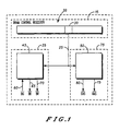
- a processor 15 comprises a programmable register 20, which is termed DCR (DRAM Control Register).
- the DCR 20 contains a status bit 30.
- the processor is coupled to various other devices via a bus 25.
- the bus 25 includes a bus grant (BG) line, a bus busy (BB) line and a bus request (BR) line, and is managed by an arbitrator (not shown).
- a bus master 35 of the arrangement is coupled to the bus 25 and includes a bus control block 40, which provides control of the bus.
- a DRAM 45 is also coupled to the bus 25 and includes a DRAM control block 50, which provides control of the DRAM 45.
- the DRAM 45 has RAS and CAS lines (not shown). If the status bit 30 of the DCR 20 is set, then the DRAM 45 is effectively private to the processor 15, and the RAS and CAS lines are driven exclusively by the processor 15.
- the bus control block 40 includes a bus grant (BG) input 60, a bus busy (BB) output 65 and a bus request (BR) 70 output coupled to the respective lines of the bus 25.
- the DRAM control block has outputs CAS 80 and RAS 75, to control the CAS and RAS lines of the DRAM 45.
- the status bit 30 of the DCR 20 is arranged to be read in parallel by the bus control block 40 and the DRAM control block 50, via the bus 25.
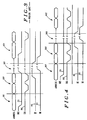
- Section 100 shows the bus release in which BR 70 is negated at the end of bus activity, BG 60 is negated by the arbitrator, and as a result BB 65 is negated by the processor 15.
- BB 65 is negated by the processor 15.
- all the processor 15 outputs become tristate (floating).
- Another processor (not shown) becomes master of the bus 25, and it asserts BB 65 to signal it's mastership. If the bit 30 is set in the DCR 20, the RAS 75 and CAS 80 lines continue to be driven by the processor 15, and do not become tristate.
- the DRAM control block 50 keeps driving the RAS line 75 asserted, when mastership is lost, as it was asserted before. Then the DRAM control block 50 starts the refresh operation (driving CAS 80 before RAS 75) immediately as the need is detected, the control block 40 controlling a DRAM refresh function of the processor 15 such that the processor 15 performs the DRAM refresh function using the RAS 75 and CAS 80 lines of the bus 25 without issuing a request for, nor assuming, control of the bus 25. The refresh is performed by asserting CAS 80 before RAS 75.
- Sections 101, 201, 301 and 401 of FIG.3 represent stages in a prior art arrangement.
- Sections 102, 202, 302 and 402 of FIG.4 represent stages found in the 'page mode' access.
- time period 402 the bus mastership is owned again by the processor 15, which starts immediately with column address driving, followed by CAS 80 assertion, and so on, thus the access time of the first access is much shorter.
- a prior art DRAM control block performs a complete access routine, as shown in section 401, with all the needed stages, row address driving, RAS assertion, column address driving, CAS assertion, etc. Again, this is also the case if the status bit 30 is not set.
Landscapes
- Engineering & Computer Science (AREA)
- Theoretical Computer Science (AREA)
- Physics & Mathematics (AREA)
- General Engineering & Computer Science (AREA)
- General Physics & Mathematics (AREA)
- Dram (AREA)
- Microcomputers (AREA)
- Memory System (AREA)
Claims (4)
- Mikroprozessor mit wenigstens RAS- und CAS-Ausgängen zur exklusiven Kopplung mit RAS- und CAS-Eingängen eines privaten DRAMs, über einen Bus, wobei der Mikroprozessor ein DRAM-Steuerregister mit wenigstens einem Bit, welches gesetzt wird, um anzuzeigen, ob der DRAM für den Mikroprozessor privat ist, eine Leseschaltung, welche das eine Bit ausliest und bestimmt, ob das Bit gesetzt ist, und eine mit der Leseschaltung gekoppelte Steuerlogikschaltung zur Steuerung von Funktionen des Mikroprozessors in Abhängigkeit davon, ob der DRAM für ihn privat ist, umfasst.
- Mikroprozessor nach Anspruch 1, wobei die Steuerlogikschaltung eine DRAM-Auffrischungsfunktion des Mikroprozessors derart steuert, dass der Mikroprozessor die DRAM-Auffrischungsfunktion unter Verwendung der RAS- und CAS-Ausgänge durchführt, ohne Ausgabe einer Anforderung nach oder einer Vermutung der Kontrolle über den Bus, wenn das eine Bit gesetzt ist, um anzuzeigen, dass der DRAM privat ist.
- Mikroprozessor nach Anspruch 1, wobei die Steuerlogikschaltung eine DRAM-Adressierungsfunktion des Mikroprozessors steuert, sodass dem Mikroprozessor, wenn das eine Bit gesetzt ist, um anzuzeigen, dass der DRAM privat ist, gestattet wird, die Kontrolle über den Bus aufzugeben, ohne die RAS- und CAS-Leitungen freizugeben, wodurch Zugriff auf den DRAM im schnellen Page-Modus ermöglich wird, wenn der Mikroprozessor das nächst Mal Kontrolle über den Bus besitzt.
- Mikroprozessorsystem, umfassend:wobei die Steuerlogikschaltung eine DRAM-Auffrischungsfunktion des Mikroprozessors derart steuert, dass der Mikroprozessor die DRAM-Auffrischungsfunktion unter Verwendung der RAS- und CAS-Leitungen des Busses durchführt, ohne Ausgabe einer Anforderung nach oder einer Vermutung der Kontrolle über den Bus, wenn das Bit gesetzt ist, und wobei die Steuerlogigschaltung eine DRAM-Adressierungsfunktion des Mikroprozessors steuert, wenn das Bit gesetzt ist, um dem Mikroprozessor, falls erwünscht, zu gestatten, die Kontrolle über den Bus aufzugeben, ohne die RAS- und CAS-Leitungen freizugeben, wodurch das nächste Mal, wenn der Mikroprozessor Kontrolle über den Bus besitzt, ein In-Page-Zugriff auf den DRAM gestattet wird.den Mikroprozessor gemäß Anspruch 1 mit Adress-, Steuer-, Daten-, RAS- und CAS-Anschlüssen, die entsprechend mit Adress-, Steuer-, Daten-, RAS- und CAS-Leitungen eines Busses gekoppelt sind;wenigstens einen DRAM, mit Adress-, Steuer-, Daten-, RAS- und CAS-Anschlüssen, welche entsprechend mit den Adress-, Steuer-, Daten-, RAS- und CAS-Leitungen des Busses gekoppelt sind, wobei der DRAM für den Mikroprozessor privat ist und die RAS- und CAS-Anschlüsse des DRAMs und des Mikroprozessors logisch miteinander verbunden sind, sodass der Mikroprozessor auf keinen anderen DRAM zugreifen kann und auf den DRAM von keinem anderen Mikroprozessor zugegriffen werden kann;
Applications Claiming Priority (3)
| Application Number | Priority Date | Filing Date | Title |
|---|---|---|---|
| GB9601693A GB2309559B (en) | 1996-01-27 | 1996-01-27 | Microprocessor and system |
| GB9601693 | 1996-01-27 | ||
| PCT/IB1996/001499 WO1997027547A2 (en) | 1996-01-27 | 1996-12-20 | Dynamic ram in a microprocessor system |
Publications (2)
| Publication Number | Publication Date |
|---|---|
| EP0818008A2 EP0818008A2 (de) | 1998-01-14 |
| EP0818008B1 true EP0818008B1 (de) | 2003-11-12 |
Family
ID=10787697
Family Applications (1)
| Application Number | Title | Priority Date | Filing Date |
|---|---|---|---|
| EP96945164A Expired - Lifetime EP0818008B1 (de) | 1996-01-27 | 1996-12-20 | Dynamisches ram in einem mikroprozessorsystem |
Country Status (9)
| Country | Link |
|---|---|
| US (1) | US6035372A (de) |
| EP (1) | EP0818008B1 (de) |
| JP (1) | JPH11503550A (de) |
| KR (1) | KR100453118B1 (de) |
| CN (1) | CN1094614C (de) |
| DE (1) | DE69630683T2 (de) |
| GB (1) | GB2309559B (de) |
| TW (1) | TW317615B (de) |
| WO (1) | WO1997027547A2 (de) |
Families Citing this family (1)
| Publication number | Priority date | Publication date | Assignee | Title |
|---|---|---|---|---|
| SE512773C2 (sv) | 1998-10-28 | 2000-05-08 | Imsys Ab | Metod och anordning för kontroll/access av DRAM-minnen |
Family Cites Families (9)
| Publication number | Priority date | Publication date | Assignee | Title |
|---|---|---|---|---|
| FR2332571A1 (fr) * | 1975-11-20 | 1977-06-17 | Labo Cent Telecommunicat | Dispositif a acces multiple a une memoire |
| IT1091633B (it) * | 1977-12-30 | 1985-07-06 | Olivetti C Ing E C Spa | Dispositivo per la gestione del l accesso diretto alla memoria di un calcolatore |
| JPH0642263B2 (ja) * | 1984-11-26 | 1994-06-01 | 株式会社日立製作所 | デ−タ処理装置 |
| US5394541A (en) * | 1990-07-17 | 1995-02-28 | Sun Microsystems, Inc. | Programmable memory timing method and apparatus for programmably generating generic and then type specific memory timing signals |
| US5448742A (en) * | 1992-05-18 | 1995-09-05 | Opti, Inc. | Method and apparatus for local memory and system bus refreshing with single-port memory controller and rotating arbitration priority |
| JPH06150023A (ja) * | 1992-11-06 | 1994-05-31 | Hitachi Ltd | マイクロコンピュータ及びマイクロコンピュータシステム |
| ATE195381T1 (de) * | 1994-06-17 | 2000-08-15 | Advanced Micro Devices Inc | Speicherübertragungsgeschwindigkeitsbegrenzung für pci-meister |
| US5873114A (en) * | 1995-08-18 | 1999-02-16 | Advanced Micro Devices, Inc. | Integrated processor and memory control unit including refresh queue logic for refreshing DRAM during idle cycles |
| US5737744A (en) * | 1995-10-13 | 1998-04-07 | Compaq Computer Corporation | Disk array controller for performing exclusive or operations |
-
1996
- 1996-01-27 GB GB9601693A patent/GB2309559B/en not_active Expired - Fee Related
- 1996-12-20 DE DE69630683T patent/DE69630683T2/de not_active Expired - Fee Related
- 1996-12-20 JP JP9526691A patent/JPH11503550A/ja not_active Ceased
- 1996-12-20 KR KR1019970706876A patent/KR100453118B1/ko not_active Expired - Fee Related
- 1996-12-20 CN CN96193623A patent/CN1094614C/zh not_active Expired - Fee Related
- 1996-12-20 WO PCT/IB1996/001499 patent/WO1997027547A2/en not_active Ceased
- 1996-12-20 US US08/817,875 patent/US6035372A/en not_active Expired - Lifetime
- 1996-12-20 EP EP96945164A patent/EP0818008B1/de not_active Expired - Lifetime
-
1997
- 1997-02-26 TW TW086102355A patent/TW317615B/zh active
Also Published As
| Publication number | Publication date |
|---|---|
| GB2309559B (en) | 2000-01-26 |
| TW317615B (de) | 1997-10-11 |
| GB9601693D0 (en) | 1996-03-27 |
| GB2309559A (en) | 1997-07-30 |
| HK1001631A1 (en) | 1998-07-03 |
| EP0818008A2 (de) | 1998-01-14 |
| KR19980703472A (ko) | 1998-11-05 |
| DE69630683T2 (de) | 2004-04-15 |
| KR100453118B1 (ko) | 2004-12-29 |
| WO1997027547A3 (en) | 1997-10-16 |
| CN1094614C (zh) | 2002-11-20 |
| WO1997027547A2 (en) | 1997-07-31 |
| DE69630683D1 (de) | 2003-12-18 |
| JPH11503550A (ja) | 1999-03-26 |
| CN1185219A (zh) | 1998-06-17 |
| US6035372A (en) | 2000-03-07 |
Similar Documents
| Publication | Publication Date | Title |
|---|---|---|
| US5463755A (en) | High-performance, multi-bank global memory card for multiprocessor systems | |
| US6233659B1 (en) | Multi-port memory device with multiple modes of operation and improved expansion characteristics | |
| US5276886A (en) | Hardware semaphores in a multi-processor environment | |
| US5226134A (en) | Data processing system including a memory controller for direct or interleave memory accessing | |
| EP0972251A1 (de) | Verfahren und gerät zur versorgung von gleichzeitigen zugriff auf gemeinschaftlichem speicher für mehrere agenten | |
| JP3039557B2 (ja) | 記憶装置 | |
| CN107257964A (zh) | 设置有整合式处理器的dram电路 | |
| US7062588B2 (en) | Data processing device accessing a memory in response to a request made by an external bus master | |
| US6292867B1 (en) | Data processing system | |
| US6529981B1 (en) | Bus arbiter | |
| EP0818008B1 (de) | Dynamisches ram in einem mikroprozessorsystem | |
| KR100353448B1 (ko) | 공유메모리 제어장치 및 방법 | |
| US5179713A (en) | Apparatus for allowing external control of local bus read using zero wait stats input of combined I/O and DRAM controller | |
| KR20240044769A (ko) | 메모리 장치 및 메모리 장치의 동작 방법 | |
| KR0176634B1 (ko) | 16비트 데이타 버스를 가진 디램 데이타 억세스 제어회로 | |
| JPS63191397A (ja) | 情報処理装置 | |
| JPH0450625B2 (de) | ||
| JPS62241045A (ja) | 記憶装置 | |
| KR100210404B1 (ko) | 공유 메모리 억세스 제어장치 | |
| JP2882202B2 (ja) | マルチポートアクセス制御回路 | |
| JPS63191398A (ja) | 情報処理装置 | |
| HK1009683A (en) | Microprocessor and system | |
| KR0145091B1 (ko) | 메모리 인터페이스 회로 | |
| JPS6280749A (ja) | I/oデバイス制御方式 | |
| JPS6224347A (ja) | バス制御装置 |
Legal Events
| Date | Code | Title | Description |
|---|---|---|---|
| PUAI | Public reference made under article 153(3) epc to a published international application that has entered the european phase |
Free format text: ORIGINAL CODE: 0009012 |
|
| AK | Designated contracting states |
Kind code of ref document: A2 Designated state(s): DE FR |
|
| 17P | Request for examination filed |
Effective date: 19980202 |
|
| 17Q | First examination report despatched |
Effective date: 20021010 |
|
| GRAH | Despatch of communication of intention to grant a patent |
Free format text: ORIGINAL CODE: EPIDOS IGRA |
|
| GRAS | Grant fee paid |
Free format text: ORIGINAL CODE: EPIDOSNIGR3 |
|
| GRAA | (expected) grant |
Free format text: ORIGINAL CODE: 0009210 |
|
| AK | Designated contracting states |
Kind code of ref document: B1 Designated state(s): DE FR |
|
| PGFP | Annual fee paid to national office [announced via postgrant information from national office to epo] |
Ref country code: FR Payment date: 20031124 Year of fee payment: 8 |
|
| REF | Corresponds to: |
Ref document number: 69630683 Country of ref document: DE Date of ref document: 20031218 Kind code of ref document: P |
|
| PLBE | No opposition filed within time limit |
Free format text: ORIGINAL CODE: 0009261 |
|
| STAA | Information on the status of an ep patent application or granted ep patent |
Free format text: STATUS: NO OPPOSITION FILED WITHIN TIME LIMIT |
|
| 26N | No opposition filed |
Effective date: 20040813 |
|
| REG | Reference to a national code |
Ref country code: FR Ref legal event code: RN |
|
| EN | Fr: translation not filed | ||
| REG | Reference to a national code |
Ref country code: FR Ref legal event code: FC |
|
| PGFP | Annual fee paid to national office [announced via postgrant information from national office to epo] |
Ref country code: DE Payment date: 20041230 Year of fee payment: 9 |
|
| ET | Fr: translation filed | ||
| REG | Reference to a national code |
Ref country code: FR Ref legal event code: TP |
|
| PG25 | Lapsed in a contracting state [announced via postgrant information from national office to epo] |
Ref country code: DE Free format text: LAPSE BECAUSE OF NON-PAYMENT OF DUE FEES Effective date: 20060701 |
|
| PG25 | Lapsed in a contracting state [announced via postgrant information from national office to epo] |
Ref country code: FR Free format text: LAPSE BECAUSE OF NON-PAYMENT OF DUE FEES Effective date: 20041231 |
|
| REG | Reference to a national code |
Ref country code: FR Ref legal event code: ST Effective date: 20110218 |