EP0813149A1 - Mécanisme de test et de diagnostic - Google Patents
Mécanisme de test et de diagnostic Download PDFInfo
- Publication number
- EP0813149A1 EP0813149A1 EP97301382A EP97301382A EP0813149A1 EP 0813149 A1 EP0813149 A1 EP 0813149A1 EP 97301382 A EP97301382 A EP 97301382A EP 97301382 A EP97301382 A EP 97301382A EP 0813149 A1 EP0813149 A1 EP 0813149A1
- Authority
- EP
- European Patent Office
- Prior art keywords
- integrated circuit
- access
- chip
- cpu
- external device
- Prior art date
- Legal status (The legal status is an assumption and is not a legal conclusion. Google has not performed a legal analysis and makes no representation as to the accuracy of the status listed.)
- Granted
Links
- 238000012360 testing method Methods 0.000 title claims abstract description 16
- 230000002093 peripheral effect Effects 0.000 claims description 17
- 238000012546 transfer Methods 0.000 description 23
- 230000006870 function Effects 0.000 description 5
- 101150073096 NRAS gene Proteins 0.000 description 3
- 238000013461 design Methods 0.000 description 2
- 238000010586 diagram Methods 0.000 description 2
- 239000000872 buffer Substances 0.000 description 1
- 230000001413 cellular effect Effects 0.000 description 1
- 238000004891 communication Methods 0.000 description 1
- 238000011161 development Methods 0.000 description 1
- 230000010354 integration Effects 0.000 description 1
- 239000004973 liquid crystal related substance Substances 0.000 description 1
- 238000012986 modification Methods 0.000 description 1
- 230000004048 modification Effects 0.000 description 1
- 238000012545 processing Methods 0.000 description 1
- 239000013598 vector Substances 0.000 description 1
Images

Classifications
-
- G—PHYSICS
- G06—COMPUTING; CALCULATING OR COUNTING
- G06F—ELECTRIC DIGITAL DATA PROCESSING
- G06F11/00—Error detection; Error correction; Monitoring
- G06F11/22—Detection or location of defective computer hardware by testing during standby operation or during idle time, e.g. start-up testing
-
- G—PHYSICS
- G06—COMPUTING; CALCULATING OR COUNTING
- G06F—ELECTRIC DIGITAL DATA PROCESSING
- G06F11/00—Error detection; Error correction; Monitoring
- G06F11/22—Detection or location of defective computer hardware by testing during standby operation or during idle time, e.g. start-up testing
- G06F11/26—Functional testing
- G06F11/273—Tester hardware, i.e. output processing circuits
- G06F11/2736—Tester hardware, i.e. output processing circuits using a dedicated service processor for test
-
- G—PHYSICS
- G06—COMPUTING; CALCULATING OR COUNTING
- G06F—ELECTRIC DIGITAL DATA PROCESSING
- G06F11/00—Error detection; Error correction; Monitoring
- G06F11/22—Detection or location of defective computer hardware by testing during standby operation or during idle time, e.g. start-up testing
- G06F11/26—Functional testing
- G06F11/273—Tester hardware, i.e. output processing circuits
- G06F11/2733—Test interface between tester and unit under test
Definitions
- the invention relates to integrated circuits, and specifically to a testing and diagnostic mechanism for use in an integrated circuit which includes a reduced instruction set computer (RISC) central processing unit (CPU) which is intended for use in portable devices which incorporates a block of on-chip memory which may be used as a cache or as RAM.
- RISC reduced instruction set computer
- CPU central processing unit
- Portable devices include electronic instruments such as personal information manager, cellular telephones, digital cameras, hand-held games, bar-code scanners, medical equipment, electronic instrumentation, and navigation systems, specifically global positioning satellite navigation systems.
- portable devices require integrated circuits which are low in cost, have low power requirements to insure long battery life, and have high standards of performance to insure that their output is accurate and usable. Additionally, the interface between the integrated circuit and the remainder of the portable device must be of a plug-and-play design so that a single type of integrated circuit may be used with a number of portable devices. Part of such flexibility is that the designer of a portable device must be able to easily incorporate the IC into the device as an off-the-shelf component, which does not require any internal modification to be used in a variety of applications.
- RISC Reduced instruction set computers
- the RISC architecture enables an IC to have a significantly smaller die size, because the smaller instruction set of the RISC technology requires fewer transistors to implement, which leads to simpler designs which consequently take less time to complete and to debug. Additionally, smaller chips having shorter signal paths mean that each instruction cycle is of a shorter duration.
- the relative size of a RISC CPU is significantly smaller than a CISC CPU, for instance, the Intel 386 SL chip is approximately 170 mm 2 , while a RISC chip having similar computational abilities is slightly more than 5 mm 2 .
- RISC-based CPUs make the RISC architecture ideal for "system-on-chip” (SOC) applications, wherein the CPU and a number of other structures are located on a single chip.
- SOC system-on-chip
- a SOC architecture will generally include the RISC CPU and some type of local RAM and/or data cache.
- the chip may include internal and external bus controllers, various types of communication ports, an interrupt controller, and pulse width modulator, various configuration registers, various timer/counter structures, and some type of output controller, such as an LCD controller.
- Such a structure may be configured in a 32-bit architecture, with associated peripherals integrated onto the chip, which integration allows the designer of the portable device incorporating the chip to reduce the development cycle and accelerate the product introduction to market.
- the chip structure may have an external 16-bit data bus with an integrated, programmable bus controller capable of supporting 8 or 16-bit SRAM, DRAM, EPROM and/or memory devices, which do not require additional buffers in order to function with the integrated circuit
- the chip may be operated at either 3.3 volts or 5 volts, which will require between 100 mW and 350 mW respectively.
- the integrated circuit may include a memory interface which provides multiple programmable chip enables, allowing users to set wait states and memory width, 8 or 16-bits wide.
- the integrated circuit provides for address decoding and DRAM control logic, which allows an external bus master to perform data transfers without requiring external address decoding or external DRAM controllers. In the case where sequential accesses are being used, the integrated circuit automatically increments the initial memory address supplied by the external bus master, thereby speeding transfers.
- the invention of this application is a testing and diagnostic mechanism which includes an external bus master controller, and which allows access of virtually all internal registers on the integrated circuit, and which allows the on-chip SRAM/DRAM controllers to access external memory.
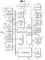
- Fig. 1 is block diagram of the system on chip structure of the invention.
- Fig. 2 is a block diagram of the pin connections between the integrated circuit of the invention and the off-chip devices connected thereto.
- IC 10 includes a 32-bit RISC CPU 12 which is connected to a 32-bit internal bus 14.
- CPU 12 is directly connected to internal bus controller 16, which in turn is connected to bus 14 and to a bus map 18.
- IC 10 further includes a local RAM (SRAM) 20, a combined instruction/data cache 22, and an external access port 24.
- SRAM local RAM
- IC 10 is intended to connect to a liquid crystal display (LCD) and to that end, includes a LCD controller 26 which is connected to an LCD panel interface 28.
- An external bus controller 30 is provided and is connected to a 26-bit external memory interface 32 and external chip selects 34.
- configuration registers 36 are provided, whose functions will be described later herein.
- configuration registers 36 are located in internal bus controller 16.
- a number of internal “peripherals” reside on integrated circuit 10, and are connected to internal bus 14, and include a universal asynchronous receiver/transmitter (UART) 38, a parallel port 40, a timer/counter 42, an interrupt controller 44, and a pulse width modulator (PWM) 46.
- UART universal asynchronous receiver/transmitter
- PWM pulse width modulator
- An external bus master 48 also referred to herein as an external device, is connected to external memory interface 32, external chip selects 34 and to an external memory 50.
- External memory 50 may include both SRAM and DRAM portions thereto.
- External memory interface 32 and external chip selects 34 are, in the preferred embodiment, a part of external bus controller 30. It will be appreciated by those of skill in the art that those objects identified by reference number 12 through 46 form parts of integrated circuit 10, while objects having reference numbers greater than 46 are off-chip devices.
- IC 10 is constructed in an 160 pin Thin Quad Flat Pack (TQFP) assembly.
- TQFP Thin Quad Flat Pack
- Fig. 2 of particular interest in the instant invention are those pins which connect to external bus master 48 and which are designated bus master request (BREQ) for transmitting a request signal bus master grant (BGR) for transmitting a grant signal, transfer request (XREQ), and transfer acknowledge (XACK).
- BREQ bus master request
- BGR request signal bus master grant
- XREQ transfer request
- XACK transfer acknowledge
- Signal flow is represented by arrowed lines connecting IC 10, external bus master 48, DRAM 50 a , SRAM 50 b and peripherals 52.
- external memory interface 32 and external chip selects 34 are physically located in external bus controller 30 in the preferred embodiment.
- Pins BREQ and XREQ are referred to herein as a request mechanism, while pins BGR and XACK are referred to herein as a grant mechanism.
- Data and/or instructions will then pass between IC 10 and the external memory and peripherals over buses for data, addresses and control functions, collectively labeled as bus 54.
- CPU 12 allows external bus master 48 to take control of external memory interface 32 as well as use on-chip SRAM/DRAM controllers, generally located in internal bus controller 16, to transfer data.
- the previously identified four dedicated signals are used to accomplish control of external interface 32.
- external bus master 48 must provide its own chip enables and CAS/RAS (column address select/row address select) signals for external memory 50, or, it must use the XREQ/XACK to access the on-chip control signals using the SRAM/DRAM controllers located in internal bus controller 16.
- External bus master 48 requests control of external memory interface 32 by asserting BREQ pin high.
- CPU 12 When CPU 12 detects that the BREQ pin is high, it completes its current bus operation and asserts BGR high, which allows external bus master 48 to take control of external interface 32. All of the on-chip components will be under control of external bus master 48, with the exception of CPU 12, which will be in an idle mode. So long as BGR is maintained high by CPU 12, external bus master 48 will have control of external memory interface 32. It should be understood that although CPU 12 is in an idle mode, IC 10 will continue to refresh the DRAM memory banks in accordance with its programming, also referred to herein as a refresh mechanism.
- external bus master 48 When external bus master 48 asserts the XREQ pin high, and assuming that BGR is also asserted high, external bus master 48 can access internal SRAM, cache, registers, DRAM controller and SRAM controller. External bus master 48 provides address, data, read/write access, and transfer size to IC 10, which uses its on-chip controllers to complete the transfer. External bus master 48 may also request IC 10 to keep track of the transfer address internally, in the a memory map register located in internal bus controller 16, and specifically in one of the configurations registers 36 therein, thus eliminating the need to provide an external address beyond that required for the first transfer. This comprises what is referred to herein as a stop/start mechanism for placing CPU 12 in an idle mode while allowing external device 48 to access on-chip registers.
- IC 10 When IC 10 detects that XREQ pin is asserted high, it provides an acknowledgment signal in the form of asserting the XACK pin high, and latching the address, data, and controls in a configuration for access by external bus master 48.
- IC 10 may take control of external memory interface 32 by asserting BGR low, which blocks external bus master 48 from controlling IC 10. When the requested transfer is completed, IC 10 will drive XACK low, place data bus 54 in a read operation and continue to assert BGR low, so long as XREQ is high. When XREQ is driven low by external bus master 48, IC 10 will assert BGR high, thereby giving external bus master 48 control of interface 32. External bus master 48 may start another transfer by driving XREQ high, or by releasing bus 54, by driving BREQ low.
- nOE is the output enable for external memory and peripherals, and allows external memory and peripherals to drive the data bus. It is asserted low during a read operation and high during a write operation. When under the control of external bus master 48, it functions as the output enable for microcontroller 12 a , which is embedded in CPU 12. nOE should be driven low during a read operation and high during a write operation by external bus master 48.
- nWE is the write enable for external memory and peripherals. During a write operation, nWE is driven low, and it is driven high during a read operation. When under the control of external bus master 48, nWE should be driven low during write operation, and high during a read operation.
- nCE/nCAS[5:0 ⁇ ] provide the chip enable (CE)/column address select (CAS) allowing direct connection to standard external memory/peripheral devices.
- the pins act as an nCAS when interfacing to DRAM 50a and acts as an nCE when interfacing to SRAM 50 b or peripheral devices 52. These pins are fully programmable by the system designer and may support byte enables.
- nCE is inactive when under the control of external bus master 48, while nCAS is active only during a refresh operation, provided that refresh is programmed into the circuit, nRAS provides row address selects allowing direct connection to DRAM 50 a , nRAS is inactive when under the control of external bus master 48.
- Pins designated as A[25:0 ⁇ ] and D[15:0 ⁇ ] are also in a high-impedance state when BGR is high.
- A[25:0 ⁇ ] designates the twenty-six external address bus pins, and allows the embedded microcontroller to provide a 26-bit address to external memory and peripherals. When under the control of external bus master 48, a 26-bit address is sent to the embedded microcontroller.
- the high order 6 bits of the address are provided by an internal programmable register, located in configuration registers 36, giving the external bus master full access to the 32-bit address space.
- D[15:0 ⁇ ] designates the 16 pin external 16-bit data bus.
- nBW is the byte-wide access pin.
- CPU 12 provides a signal to external memory 50 and peripherals 52 which indicate the data size of the data transfer.
- nBW may be used by an external address controller to generate extra chip/byte enables.
- the extemal bus master indicates the transfer size.
- CPU 12 or external bus master 48 a low asserted on pin nBW indicates a byte transfer, and a high asserted on pin nBW indicates a half word (16-bit transfer).
- Pin nBB is the byte boot pin, which is used to select between 8-bit or 16-bit for the boot memory.
- external bus master 48 may provide its own address to microcontroller 12 a on bus 54, in which case pin nBB is asserted low, and the high order 6 bits of the address are provided by an internal programmable register, identified as external bus master extension register (EBMER) and located in configuration registers 36.
- EBMER external bus master extension register
- the external bus master 48 may also request the embedded microcontroller to keep track of the transfer address internally, in which case pin nBB should be asserted high.
- Microcontroller 12 a adjusts the internal address as a function of the transfer size specified by external bus master 48 (nBW).
- An external bus master register is used to expand addresses from external bus master 48 from 26-bits to 32-bits, thus allowing access to the entire address space provided by CPU 12.
- the internal 32-bit address is formed by adding an address extension of six bits to the 26-bit address on pins A[25:0 ⁇ ]. Every time external bus master 48 provides an external address and nBB is asserted low, IC 10 captures the external address and forms a 32-bit internal address by combining the external bus master address and the address extension found in the external bus master extension register. Once the access is completed, IC 10 updates the new address according to the transfer size specified by external bus master 48 via nBW, to point to the next addressable location. If external bus master 48 is conducting sequential transfers, this structure allows IC 10 to supply future addresses.
- the address extension initially loaded into the external bus master extension register has a logical value of "111111", allowing external bus master 48 to access the upper region of memory which includes system and peripheral registers, including the external bus master extension register, local SRAM, cache, and exception vectors.
- the external bus master extension register may be updated by a store command or by external bus master 48. Once the value in external bus master extension register is changed from "111111", the external bus master 48 is not allowed to access the external bus master register extension or the upper region of memory.
- the foregoing structures comprise what is referred to herein as an automatic address incrementation means.
- any register on IC 10 may be used for diagnostics, to determine the contents of a register at any particular point in the operation of IC 10, for programming, which allows a user to insert a specific address or data into a register, or for testing, which allows a designer to confirm that a specific register contains a given content at any point in time during operation.
- This system may be particularly useful where IC 10 is used as part of a charge-coupled-device (CCD) camera, wherein pixel data is received from the CCD and is transferred into memory. Such transfer is generally too fast to be manageable by a conventional interrupt system.
- the starting address may be provided, either by IC 10 or from some external control, depending on the particular address map, which will allow IC 10 to transfer data at a high rate of speed from the CCD into memory.
Applications Claiming Priority (2)
| Application Number | Priority Date | Filing Date | Title |
|---|---|---|---|
| US62026996A | 1996-03-22 | 1996-03-22 | |
| US620269 | 1996-03-22 |
Publications (2)
| Publication Number | Publication Date |
|---|---|
| EP0813149A1 true EP0813149A1 (fr) | 1997-12-17 |
| EP0813149B1 EP0813149B1 (fr) | 2002-06-05 |
Family
ID=24485265
Family Applications (1)
| Application Number | Title | Priority Date | Filing Date |
|---|---|---|---|
| EP97301382A Expired - Lifetime EP0813149B1 (fr) | 1996-03-22 | 1997-03-03 | Mécanisme de test et de diagnostic |
Country Status (5)
| Country | Link |
|---|---|
| US (1) | US5825784A (fr) |
| EP (1) | EP0813149B1 (fr) |
| JP (1) | JPH09258998A (fr) |
| KR (1) | KR100261787B1 (fr) |
| DE (1) | DE69712982T2 (fr) |
Families Citing this family (8)
| Publication number | Priority date | Publication date | Assignee | Title |
|---|---|---|---|---|
| JP2002023811A (ja) * | 2000-07-11 | 2002-01-25 | Mitsubishi Electric Corp | フィールド機器制御装置およびそのコネクタの配線接続方法 |
| JP2002267721A (ja) * | 2001-03-09 | 2002-09-18 | Mitsubishi Electric Corp | Cpu内蔵ram混載lsiのテスト装置および方法 |
| EP1477903A3 (fr) * | 2003-05-13 | 2004-12-29 | Freescale Semiconductor, Inc. | Système de mémoire d'un radiotéléphone |
| US8832346B2 (en) * | 2003-06-16 | 2014-09-09 | Nvidia Corporation | Data packing and unpacking engine |
| US8095699B2 (en) * | 2006-09-29 | 2012-01-10 | Mediatek Inc. | Methods and apparatus for interfacing between a host processor and a coprocessor |
| US8438432B2 (en) * | 2010-08-25 | 2013-05-07 | Vixs Systems, Inc. | DRAM memory controller with built-in self test and methods for use therewith |
| US9251874B2 (en) * | 2010-12-21 | 2016-02-02 | Intel Corporation | Memory interface signal reduction |
| US9720827B2 (en) * | 2014-11-14 | 2017-08-01 | Intel Corporation | Providing multiple memory modes for a processor including internal memory |
Citations (4)
| Publication number | Priority date | Publication date | Assignee | Title |
|---|---|---|---|---|
| US4245307A (en) * | 1979-09-14 | 1981-01-13 | Formation, Inc. | Controller for data processing system |
| JPS626488A (ja) * | 1985-06-29 | 1987-01-13 | Toshiba Corp | メモリリフレツシユ回路 |
| EP0636976A1 (fr) * | 1993-07-28 | 1995-02-01 | Koninklijke Philips Electronics N.V. | Microcontrôleur avec support de débagage en hardware par des extensions à boundary scan |
| EP0652516A1 (fr) * | 1993-11-03 | 1995-05-10 | Advanced Micro Devices, Inc. | Microprocesseur intégré |
Family Cites Families (6)
| Publication number | Priority date | Publication date | Assignee | Title |
|---|---|---|---|---|
| US4010448A (en) * | 1974-10-30 | 1977-03-01 | Motorola, Inc. | Interrupt circuitry for microprocessor chip |
| US5212775A (en) * | 1990-01-04 | 1993-05-18 | National Semiconductor Corporation | Method and apparatus for observing internal memory-mapped registers |
| US5251304A (en) * | 1990-09-28 | 1993-10-05 | Motorola, Inc. | Integrated circuit microcontroller with on-chip memory and external bus interface and programmable mechanism for securing the contents of on-chip memory |
| US5408639A (en) * | 1992-07-21 | 1995-04-18 | Advanced Micro Devices | External memory access control for a processing system |
| GB2282244B (en) * | 1993-09-23 | 1998-01-14 | Advanced Risc Mach Ltd | Integrated circuit |
| US5537355A (en) * | 1994-11-30 | 1996-07-16 | Sony Corporation Of Japan | Scheme to test/repair multiple large RAM blocks |
-
1996
- 1996-12-27 JP JP8349576A patent/JPH09258998A/ja active Pending
- 1996-12-30 KR KR1019960082482A patent/KR100261787B1/ko not_active IP Right Cessation
-
1997
- 1997-03-03 DE DE69712982T patent/DE69712982T2/de not_active Expired - Lifetime
- 1997-03-03 EP EP97301382A patent/EP0813149B1/fr not_active Expired - Lifetime
- 1997-09-17 US US08/932,151 patent/US5825784A/en not_active Expired - Lifetime
Patent Citations (4)
| Publication number | Priority date | Publication date | Assignee | Title |
|---|---|---|---|---|
| US4245307A (en) * | 1979-09-14 | 1981-01-13 | Formation, Inc. | Controller for data processing system |
| JPS626488A (ja) * | 1985-06-29 | 1987-01-13 | Toshiba Corp | メモリリフレツシユ回路 |
| EP0636976A1 (fr) * | 1993-07-28 | 1995-02-01 | Koninklijke Philips Electronics N.V. | Microcontrôleur avec support de débagage en hardware par des extensions à boundary scan |
| EP0652516A1 (fr) * | 1993-11-03 | 1995-05-10 | Advanced Micro Devices, Inc. | Microprocesseur intégré |
Non-Patent Citations (1)
| Title |
|---|
| PATENT ABSTRACTS OF JAPAN vol. 011, no. 177 (P - 583) 6 June 1987 (1987-06-06) * |
Also Published As
| Publication number | Publication date |
|---|---|
| EP0813149B1 (fr) | 2002-06-05 |
| US5825784A (en) | 1998-10-20 |
| KR970066598A (ko) | 1997-10-13 |
| DE69712982T2 (de) | 2002-11-28 |
| JPH09258998A (ja) | 1997-10-03 |
| KR100261787B1 (ko) | 2000-07-15 |
| DE69712982D1 (de) | 2002-07-11 |
Similar Documents
| Publication | Publication Date | Title |
|---|---|---|
| US5826106A (en) | High performance multifunction direct memory access (DMA) controller | |
| US6055584A (en) | Processor local bus posted DMA FlyBy burst transfers | |
| US5525971A (en) | Integrated circuit | |
| US6591294B2 (en) | Processing system with microcomputers each operable in master and slave modes using configurable bus access control terminals and bus use priority signals | |
| US5642489A (en) | Bridge between two buses of a computer system with a direct memory access controller with accessible registers to support power management | |
| US6131127A (en) | I/O transactions on a low pin count bus | |
| EP0697663A2 (fr) | Dispositif et méthode de traitement pour ordinateur utilisant une architecture harvard améliorée | |
| CN108304334B (zh) | 应用处理器和包括中断控制器的集成电路 | |
| EP0658852A2 (fr) | Système d'ordinateur avec un bus local modifié | |
| US5416916A (en) | Structure for enabling direct memory-to-memory transfer with a fly-by DMA unit | |
| US6122679A (en) | Master DMA controller with re-map engine for only spawning programming cycles to slave DMA controllers which do not match current programming cycle | |
| US5859649A (en) | Data processing system having display controller with bursting direct memory access | |
| EP0813149B1 (fr) | Mécanisme de test et de diagnostic | |
| US5687131A (en) | Multi-mode cache structure | |
| KR20010006839A (ko) | 마이크로 컴퓨터, 전자 기기 및 에뮬레이션 방법 | |
| US7310717B2 (en) | Data transfer control unit with selectable transfer unit size | |
| US6665748B1 (en) | Specialized PCMCIA host adapter for use with low cost microprocessors | |
| KR960001023B1 (ko) | 이기종 버스시스템에서의 버스 공유방법 및 버스 스와핑장치 | |
| EP0813152B1 (fr) | Mécanisme de protection de mémoire | |
| TW321723B (en) | Testing and diagnostic mechanism | |
| US20040024929A1 (en) | System and method for controlling communication on a signal bus | |
| JPH02207363A (ja) | データ転送制御方式、デバイスコントローラ、およびメモリ・コントローラ | |
| JPH04109351A (ja) | Dmaコントローラ | |
| Salcic et al. | Rapid Prototyping Using FPLDS-Vuman Case Study | |
| EP0784823A2 (fr) | Processeur de signaux numeriques |
Legal Events
| Date | Code | Title | Description |
|---|---|---|---|
| PUAI | Public reference made under article 153(3) epc to a published international application that has entered the european phase |
Free format text: ORIGINAL CODE: 0009012 |
|
| AK | Designated contracting states |
Kind code of ref document: A1 Designated state(s): DE FR GB |
|
| 17P | Request for examination filed |
Effective date: 19980226 |
|
| 17Q | First examination report despatched |
Effective date: 20010103 |
|
| GRAG | Despatch of communication of intention to grant |
Free format text: ORIGINAL CODE: EPIDOS AGRA |
|
| GRAG | Despatch of communication of intention to grant |
Free format text: ORIGINAL CODE: EPIDOS AGRA |
|
| GRAH | Despatch of communication of intention to grant a patent |
Free format text: ORIGINAL CODE: EPIDOS IGRA |
|
| GRAH | Despatch of communication of intention to grant a patent |
Free format text: ORIGINAL CODE: EPIDOS IGRA |
|
| GRAA | (expected) grant |
Free format text: ORIGINAL CODE: 0009210 |
|
| AK | Designated contracting states |
Kind code of ref document: B1 Designated state(s): DE FR GB |
|
| REG | Reference to a national code |
Ref country code: GB Ref legal event code: FG4D |
|
| REF | Corresponds to: |
Ref document number: 69712982 Country of ref document: DE Date of ref document: 20020711 |
|
| ET | Fr: translation filed | ||
| PLBE | No opposition filed within time limit |
Free format text: ORIGINAL CODE: 0009261 |
|
| STAA | Information on the status of an ep patent application or granted ep patent |
Free format text: STATUS: NO OPPOSITION FILED WITHIN TIME LIMIT |
|
| 26N | No opposition filed |
Effective date: 20030306 |
|
| PGFP | Annual fee paid to national office [announced via postgrant information from national office to epo] |
Ref country code: FR Payment date: 20120319 Year of fee payment: 16 |
|
| PGFP | Annual fee paid to national office [announced via postgrant information from national office to epo] |
Ref country code: GB Payment date: 20120307 Year of fee payment: 16 |
|
| PGFP | Annual fee paid to national office [announced via postgrant information from national office to epo] |
Ref country code: DE Payment date: 20120404 Year of fee payment: 16 |
|
| GBPC | Gb: european patent ceased through non-payment of renewal fee |
Effective date: 20130303 |
|
| REG | Reference to a national code |
Ref country code: FR Ref legal event code: ST Effective date: 20131129 |
|
| REG | Reference to a national code |
Ref country code: DE Ref legal event code: R119 Ref document number: 69712982 Country of ref document: DE Effective date: 20131001 |
|
| PG25 | Lapsed in a contracting state [announced via postgrant information from national office to epo] |
Ref country code: GB Free format text: LAPSE BECAUSE OF NON-PAYMENT OF DUE FEES Effective date: 20130303 Ref country code: FR Free format text: LAPSE BECAUSE OF NON-PAYMENT OF DUE FEES Effective date: 20130402 Ref country code: DE Free format text: LAPSE BECAUSE OF NON-PAYMENT OF DUE FEES Effective date: 20131001 |