EP0810775A2 - Verbesserungsverfahren zur Kompensation von defekten Elementen in einer Bildelementmatrize einer Bildaufnahmevorrichtung - Google Patents
Verbesserungsverfahren zur Kompensation von defekten Elementen in einer Bildelementmatrize einer Bildaufnahmevorrichtung Download PDFInfo
- Publication number
- EP0810775A2 EP0810775A2 EP97113834A EP97113834A EP0810775A2 EP 0810775 A2 EP0810775 A2 EP 0810775A2 EP 97113834 A EP97113834 A EP 97113834A EP 97113834 A EP97113834 A EP 97113834A EP 0810775 A2 EP0810775 A2 EP 0810775A2
- Authority
- EP
- European Patent Office
- Prior art keywords
- exposure
- array
- sliding window
- pixel
- row
- Prior art date
- Legal status (The legal status is an assumption and is not a legal conclusion. Google has not performed a legal analysis and makes no representation as to the accuracy of the status listed.)
- Granted
Links
Images


Classifications
-
- G—PHYSICS
- G03—PHOTOGRAPHY; CINEMATOGRAPHY; ANALOGOUS TECHNIQUES USING WAVES OTHER THAN OPTICAL WAVES; ELECTROGRAPHY; HOLOGRAPHY
- G03G—ELECTROGRAPHY; ELECTROPHOTOGRAPHY; MAGNETOGRAPHY
- G03G15/00—Apparatus for electrographic processes using a charge pattern
- G03G15/04—Apparatus for electrographic processes using a charge pattern for exposing, i.e. imagewise exposure by optically projecting the original image on a photoconductive recording material
- G03G15/043—Apparatus for electrographic processes using a charge pattern for exposing, i.e. imagewise exposure by optically projecting the original image on a photoconductive recording material with means for controlling illumination or exposure
-
- H—ELECTRICITY
- H04—ELECTRIC COMMUNICATION TECHNIQUE
- H04N—PICTORIAL COMMUNICATION, e.g. TELEVISION
- H04N1/00—Scanning, transmission or reproduction of documents or the like, e.g. facsimile transmission; Details thereof
- H04N1/40—Picture signal circuits
- H04N1/401—Compensating positionally unequal response of the pick-up or reproducing head
- H04N1/4015—Compensating positionally unequal response of the pick-up or reproducing head of the reproducing head
-
- G—PHYSICS
- G03—PHOTOGRAPHY; CINEMATOGRAPHY; ANALOGOUS TECHNIQUES USING WAVES OTHER THAN OPTICAL WAVES; ELECTROGRAPHY; HOLOGRAPHY
- G03G—ELECTROGRAPHY; ELECTROPHOTOGRAPHY; MAGNETOGRAPHY
- G03G15/00—Apparatus for electrographic processes using a charge pattern
-
- G—PHYSICS
- G06—COMPUTING; CALCULATING OR COUNTING
- G06K—GRAPHICAL DATA READING; PRESENTATION OF DATA; RECORD CARRIERS; HANDLING RECORD CARRIERS
- G06K15/00—Arrangements for producing a permanent visual presentation of the output data, e.g. computer output printers
- G06K15/02—Arrangements for producing a permanent visual presentation of the output data, e.g. computer output printers using printers
- G06K15/12—Arrangements for producing a permanent visual presentation of the output data, e.g. computer output printers using printers by photographic printing, e.g. by laser printers
- G06K15/1238—Arrangements for producing a permanent visual presentation of the output data, e.g. computer output printers using printers by photographic printing, e.g. by laser printers simultaneously exposing more than one point
-
- H—ELECTRICITY
- H04—ELECTRIC COMMUNICATION TECHNIQUE
- H04N—PICTORIAL COMMUNICATION, e.g. TELEVISION
- H04N1/00—Scanning, transmission or reproduction of documents or the like, e.g. facsimile transmission; Details thereof
- H04N1/40—Picture signal circuits
- H04N1/40025—Circuits exciting or modulating particular heads for reproducing continuous tone value scales
- H04N1/40031—Circuits exciting or modulating particular heads for reproducing continuous tone value scales for a plurality of reproducing elements simultaneously
-
- G—PHYSICS
- G06—COMPUTING; CALCULATING OR COUNTING
- G06K—GRAPHICAL DATA READING; PRESENTATION OF DATA; RECORD CARRIERS; HANDLING RECORD CARRIERS
- G06K2215/00—Arrangements for producing a permanent visual presentation of the output data
- G06K2215/0082—Architecture adapted for a particular function
- G06K2215/0085—Error recovery
Definitions
- This invention relates generally to electrophotographic printing with a spatial light modulator (SLM), and more particularly to generating grayscale images with data that represents time integration values and that is selected for delivery to the SLM with a sliding window memory.
- SLM spatial light modulator
- the invention relates to the compensation of defects in such an environment.
- SLM Spatial light modulator
- an SLM is an array of light-emitting, light-transmitting or light-reflecting elements, which are individually addressable, usually with electronic signals.
- Many SLMs are binary, having an addressing scheme that switches its elements to either to an "on” or an “off” state to form the image.
- DMD digital micro-mirror device
- the DMD has an array of hundreds or thousands of tiny tilting mirrors. To permit the mirrors to tilt, each is attached to one or more hinges mounted on support posts, and spaced by means of an air gap over underlying addressing circuitry.
- the addressing circuitry provides electrostatic forces, which cause each mirror to selectively tilt.
- the DMD is addressed with exposure data and in accordance with the data, light is selectively reflected or not reflected from each mirror to the printer drum.
- OPC organic photoconductive
- the drum is either charged or discharged to attract toner, with the charging or discharging accomplished by reflecting light onto the drum.
- a page is printed by exposing the drum, array-by-array.
- the drum rotates in a direction known as the process direction, and overlapping arrays of data are superposed on the drum to accumulate charge (or discharge) on the drum by integration of several exposures. Thus, charge is integrated over time.
- the toner is then transferred to paper.
- the amount of toner that clings to any point on the drum is a function of the level of charge (or discharge) on that point.
- grayscale printing (generating many shades of gray) could be done simply by adjusting the charge or discharge of each point so as to control the amount of toner at each point, with the desired gray scale then being printed.
- this approach only a limited number of shades of gray can be achieved.
- Grayscales of the kind required for high resolution imaging are produced by taking advantage of the ability of the human eye to integrate over an area. For example, a mid-level gray dot will be perceived if smaller dots of lighter and darker than mid-level gray are printed next to each other. For example, if two light gray dots of 1/600 of an inch square and two dark gray dots of 1/600 of an inch square are printed in a square, the eye will integrate the four dots and perceive a mid-gray dot of 1/300 of an inch square.
- SLMs can be modulated in at least two ways: intensity modulation and spatial modulation. These techniques may be combined. These techniques are described in U.S. Patent No. 5,461,411, entitled “Process and Architecture for Digital Micromirror Printer", assigned to Texas Instruments Incorporated and incorporated herein by reference. For each image to be exposed, the SLM generates a series of microimages, which permit pixel-by-pixel variations in the duration of exposure and the area exposed.
- SLM In both intensity modulation and spatial modulation, the SLM must be addressed so that it exposes each pixel at the appropriate times.
- a goal of SLM-based printing systems is to accomplish this addressing with a minimum of processing and memory requirements.
- the present invention is directed to a method of compensating for defective elements of a pixel array imaging device used for exposing a photoconductive printer drum, which elements are "stuck on".
- the method comprises the steps of determining a defect background value; adding said defect background value to an exposure value of each said pixel, thereby generating a backgrounded exposure value for each said pixel; subtracting a defect intensity value from exposure values of pixels affected by said defective elements, thereby providing an array of exposure data; storing said array of exposure data in a sliding window memory, said sliding window memory having a predetermined number of addressable rows, each of said rows for storing a row of said array of exposure data; generating a microimage on said drum, by addressing elements of a pixel array imaging device in accordance with said exposure data; decrementing said exposure data to account for said microimage, except to the extent that said exposure data is associated with a defective element; readdressing each row of said array of exposure data to a next row of said sliding window memory; addressing a new row of exposure
- the method of compensating for defective elements of a pixel array imaging device used for exposing a photoconductive printer drum, which elements are "stuck on” comprises the steps of determining a defect background value; adding said defect background value to an exposure value of each said pixel, thereby generating a backgrounded exposure value for each said pixel; storing an array of exposure data in a sliding window memory, said sliding window memory having a predetermined number of addressable rows, each of said rows for storing a row of said array of exposure data; generating a microimage on said drum, by addressing elements of a pixel array imaging device in accordance with said exposure data; decrementing said exposure data to account for said microimage and to account for said defective elements; readdressing each row of said array of exposure data to a next row of said sliding window memory; addressing a new row of exposure data as a last row of said sliding window memory; repeating said generating, decrementing, readdressing, and addressing steps until all of said image is exposed; and eliminating said background exposure level
- Another aspect of the invention is a method of compensating for defective elements of a spatial light modulator (SLM) used for exposing a photoconductive printer drum, which elements are "stuck on”, which method comprises the steps of providing extra rows of said SLM, which extra rows comprise a white balancing area; determining a number of said defective pixel-generating elements in each column of said SLM; for each said defective element in a column of said SLM, addressing elements in a corresponding column of said white balancing area as "off”; and addressing all other elements in said white balancing area as "on".
- SLM spatial light modulator
- FIGURE 1 illustrates the relationship between an OPC drum and a DMD array.
- FIGURE 2 illustrates an array of contone data to be printed on a page.
- FIGURE 3 is a graphical representation, in time, of the relationship between lines on an OPC drum and a DMD array.
- FIGURE 4 is a row integration sliding window array according to the teachings of the present invention.
- FIGURE 5 is a row integration gray scale lookup table according to the teachings of the present invention.
- FIGURE 6 is a microimage array according to the teachings of the present invention.
- FIGURE 7 is a row integration sliding window array after decrementing and sliding according to the teachings of the present invention.
- FIGURE 8 is a flow diagram for a sliding window approach according to the teachings of the present invention.
- FIGURE 9 is a graphical representation, in time, of the relationship between lines on an OPC drum and a DMD array.
- FIGURE 10 is a multiple intensities sliding window array according to the teachings of the present invention.
- FIGURE 11 is a lookup table for gray scale using four light intensities according to the teachings of the present invention.
- FIGURE 12 is a graphical representation, in time, of the relationship between lines on an OPC drum and a DMD array.
- FIGURE 13 is a multiple phases and intensities sliding window array according to the teachings of the present invention.
- FIGURE 14 is a gray scale lookup table with two phases and two intensities according to the teachings of the present invention.
- FIGURE 15 is a graphical representation, in time, of the relationship between lines on an OPC drum and a DMD array.
- FIGURE 16 is a gray scale lookup table for a two intensities, four phase system according to the teachings of the present invention.
- FIGURE 17 is a pulse duration sliding window array according to the teachings of the present invention.
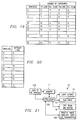
- FIGURE 18 is a gray scale lookup table for a three phase pulse duration modulation system according to the teachings of the present invention.
- FIGURE 19 is a gray scale lookup table for an anamorphic two duration pulse duration modulation system according to the teachings of the present invention.
- FIGURE 20 is an alternative embodiment gray scale lookup table for a two intensity four phase system according to the teachings of the present invention.
- FIGURE 21 is a block diagram of a printer according to the teachings of the present invention.
- the following description is in terms of printer systems whose spatial light modulators (SLMs) are digital micro-mirror devices (DMDs).
- SLMs spatial light modulators
- DMDs digital micro-mirror devices
- the same concepts apply to printer systems that use other types of pixel array imaging devices.
- a printer system having an array of liquid crystal elements instead of a DMD array could used.
- the image is generated by mirror elements, but for pixel array devices in general, the terms "pixels" or "elements” are often used.
- the pixels of the array usually have a one-to-one correspondence with the pixels of the image, and the context of the following description indicates where this is not the case.
- FIGURE 1 illustrates a printer exposure unit 10 having a DMD 12 and a memory 13, in accordance with the present invention.
- DMD 12 individual reflecting elements of DMD 12 are referred to as “mirrors” or “mirror elements”.
- each row of DMD 12 could be staggered, such that the individual mirror elements are offset from row to row.
- advantage can be taken of spatial modulation in the cross-process direction, as disclosed in U.S. Patent No.5,453,778, entitled “Method and Apparatus for Spatial Modulation in the Cross-Process Direction,” which is assigned to Texas Instruments Incorporated, and incorporated herein by reference.
- DMD 12 has only 4 rows of mirror elements with 16 mirror elements per row. However, for practical applications, DMD 12 may have many more rows and columns. A typical DMD 12 might have 1000 or more mirror elements per row.
- Light from a light source 14 is reflected by DMD 12 onto an OPC drum 16, in accordance with the "on" or “off” state of each mirror element. This state is determined by data delivered from an exposure data memory 13. As explained below, memory 13 delivers one bit of data for each mirror to be addressed during a single line period. The image is reflected and focused through an optics unit 18. As shown in FIGURE 1, light from DMD 12 falls on OPC drum 16, with each mirror providing light for one pixel on the image.
- drum 16 Because drum 16 is rotating, light is received at a line of pixels on drum 16 from different rows of mirrors on DMD 12 at different times.
- the desired amount of exposure time can be accomplished by pulsing light source 14 or by leaving light source 14 on and switching the mirrors on or off at the appropriate times.
- the "on" or “off” state of the mirrors or the amplitude of light source 14 is updated once for every line of drum movement (each line period). However, many other update speeds may be used without departing from the scope of the invention.
- pixel 20 is exposed by a column of four mirrors 22-28 during four different time intervals as drum 16 rotates. Each time interval is a "line period”.
- pixel 46 is exposed by mirrors 38-44.
- Pixel 21, which is in the second row of pixels, is exposed by mirrors 22-28 but one line period later than pixel 20.
- each pixel of drum 16 is exposed in accordance with data delivered to four different mirrors in the same column of DMD 12 during four successive line periods.
- the relationship between the light exposure on the drum and the final gray scale is not necessarily linear, and can be determined experimentally or through modeling.
- the relationship can be expressed as a lookup table that relates gray scale to the light exposure needed on each phase.
- grayscale will refer to the cumulative light exposure at a pixel, rather than the actual perceived grayscale. Due to the non-linear relationship described above, it is possible that two different exposure profiles may result in the same perceived grayscale, and alternatively that two different profiles with the same cumulative exposure may result in different perceived grayscales.
- the mirrors shown in FIGURE 1 are exemplary only, and that other shaped mirrors may be used as well.
- the mirrors shown in FIGURE 1 are square, and are referred to as isomorphic DMDs.
- Anamorphic DMDs may also be used.
- rectangular DMDs having half the height of those shown in array 12 may also be used.
- the optics 18 may be used to make isomorphic mirrors effectively anamorphic, and vice versa.
- FIGURE 2 illustrates a set of greyscale values, representing an image to be printed.
- a number of lines are to be printed, designated as Line 0 through Line L-1 .
- Each row of values corresponds to a line, and contains the greyscale data for each pixel on the line.
- each line includes n pixels.
- the first row of the array of FIGURE 2 Line 0 , contains data for pixel P 0,0 through P 0,n-1 .
- these greyscale values are stored in memory 13 and used as the basis for microimage data for delivery to DMD 12. The microimages are time-integrated to result in the desired grayscale image.
- FIGURE 3 illustrates a method of successively exposing each pixel of the image by light from mirror elements in the same column of DMD 12. For example, a line of pixels will first be exposed by a first row of mirror elements, then exposed by a second row of mirror elements, followed by exposures from two succeeding rows of mirror elements. This accumulates exposure on particular pixels, thus allowing for the printing of different gray scales.
- the mirrors M0 - M3 might be any column of four mirrors on DMD 12, such as mirrors 22, 24, 26, and 28 of FIGURE 1.
- the DMD 12 is addressed with a new set of data.
- the data delivered to each mirror is binary in the sense that it indicates whether that mirror should be ON or OFF during that exposure period.
- the binary data (0 or 1 values) for all mirrors of DMD to be addressed during a single exposure period is referred to herein as "microimage" data.
- microimage data In the example of FIGURE 3, four microimages, m 0 - m 3 , are superposed to represent the final image.
- FIGURE 3 illustrates the complete exposure of only one pixel (on Line 0), all other pixels are exposed in the same manner. Pixels in the same column are exposed by the same mirror elements, but with other microimage values. Pixels in different columns are exposed by different mirror elements.
- the microimages can be visualized as moving down the "page" represented by pixels on drum 16.
- DMD 12 moves down the page one line at a time.
- DMD 12 receives new data and generates a new microimage.
- all but the top one of the previously exposed lines of the image are part of the new microimage.
- a new line of the image is also part of the new microimage.
- the present invention involves the retrieval of data from memory 13 for providing the microimage data to DMD 12.
- the memory 13 uses pointers to simulate a sliding window, which at any given time contains the greyscale data from which the current microimage is derived.
- the pointers are reassigned so that the sliding window slides down the page.
- each pixel's greyscale value is updated to account for the previous microimage exposure of that pixel's total exposure.
- FIGURE 4 illustrates a sliding window array for a row integration system. This array is stored in memory 13. As shown in FIGURE 4, the sliding window array has R rows, designated ROW 0 through ROW R-1 . The array contains an exposure value for each pixel to be exposed. The number of rows in the sliding window corresponds to the number of rows of the microimages generated by DMD 12.
- FIGURE 5 illustrates a look-up table for obtaining the exposure values in the sliding window array of FIGURE 4.
- the lookup table maps a desired grayscale into exposure values to be stored in the sliding window array.
- Each exposure value is the number of exposures that a pixel is to receive.
- the number of sliding window array rows must be at least as great as the highest number of exposures in the lookup table.
- the lookup table of FIGURE 5 has 9 as the highest exposure value, and thus at least 9 sliding window array rows are needed.
- the sliding window array is initialized with all zeros.
- the exposure values for the first line of the image are then addressed as the last row of the array.
- the array rows are identified with pointers, so that no actual copying of data from one location from another is required.
- the invention could also be implemented with copying, such that data is written into appropriate locations in memory.
- FIGURE 6 illustrates how microimage data is obtained from the exposure values of FIGURE 4.
- all of the mirrors of DMD 12 are OFF except the appropriate mirrors in the last row of DMD 12. This last row will expose the first line of the image during the first exposure period.
- the mirrors of DMD ROW R-1 will be ON or OFF, depending on the information in ROW R-1 of the sliding window array. As illustrated, if the exposure value for a mirror is 3 1, the mirror is ON. If the exposure value is 0, the mirror is OFF.
- FIGURE 7 illustrates the sliding window array of FIGURE 4, but after the first exposure.
- the exposure values of ROW R-1 have been decremented to reflect the first exposure.
- ROW R-1 has been readdressed as ROW R-2 .
- a new row of exposure values is addressed as ROW R-1 , for the second line of the image, which is Line 1 of FIGURE 2.
- FIGURE 8 illustrates a generalized process for using a sliding window array of exposure values in accordance with the invention. It describes the process described above in connection with FIGUREs 3 - 7 for row integration, as well as the processes described below for other types of greyscale printing.
- Step 80 is initializing the sliding window array with 0s.
- step 82 the sliding window array is addressed for the first microimage.
- row ROW R-1 is loaded with exposure values. All other rows of the sliding window array remain initialized at zero.
- a microimage is generated based on the exposure values in the sliding window array.
- the sliding window array is decremented. Decrementing is accomplished by subtracting one unit from each exposure value in the sliding window array that corresponds to a pixel that has been exposed.
- Rows of exposure values receive addresses for preceding rows of the array, such that each row receives exposure values from the next row down.
- ROW K ROW K+1 .
- a new row of exposure values for the next line to be printed is addressed as the last row of the sliding array.
- ROW R-1 Line t . This process continues until all lines of the image have been exposed.
- FIGURE 9 illustrates a multiple intensity approach to grayscale printing. Like FIGURE 3, FIGURE 9 illustrates exposure of several pixels in one column of an OPC drum. For purposes of illustration, the exposures are spread horizontally, but are actually superposed.
- the intensity of light source 14 of FIGURE 1 is cycled through different intensities.
- the representation of FIGURE 9 illustrates four different intensities, I 1 , I 2 , I 4 , I 8 , where the second intensity is twice the first, the third intensity is twice the second, and the fourth intensity is twice the third.
- FIGURE 10 illustrates the sliding window array for the multiple intensities approach of FIGURE 9.
- Each row of the sliding window array includes exposure data for each intensity for each pixel on that row.
- each row is a two-dimensional array in itself, having p columns, where p is the number of pixels in a row, and i rows, where i is the number of different intensity levels available in the system.
- the exposure data for each intensity corresponds to the number of exposures that each pixel should receive at a particular intensity level.
- This information is received from a lookup table such as that shown in FIGURE 11.
- the lookup table of FIGURE 11 maps the desired grayscale from the data of FIGURE 2 into the number of exposures required at each intensity level.
- the sliding window array of FIGURE 10 shows pixel P 0 of ROW R-1 having a grayscale level of 2, pixel P 1 having a grayscale value of 31, and pixel P P-1 having a grayscale value of 63.
- a microimage is generated based on the sliding window array of FIGURE 10, followed by decrementing and sliding the sliding window array.
- decrementing is accomplished by subtracting one from the exposure value for the appropriate intensity of each pixel that has a value greater than zero.
- the I 1 data value for pixel P 0 of ROW R-1 will not be decremented, because it is zero.
- the I 1 data value is decremented from the three to two, and for pixel P P-1 , the data value I 1 is decremented from five to four.
- FIGURE 12 illustrates a pulse position approach to grayscale printing. Like FIGUREs 3 and 9, FIGURE 12 illustrates the relationship between a column of pixels of several lines on drum 16 and mirrors in a column of DMD 12. Pulse positioning is used to control where light from each of the mirrors falls on the drum.
- the "on" time for every other microimage is alternatively delayed or advanced by 1/4 pixel height.
- the mirror that overlaps line L and line L+1 is counted as contributing to Line L.
- a particular pixel has two phases. These phases can be created by controlling when the light is reflected onto the OPC drum. This control can be performed by pulsing the light source at the desired times, or by using the mirrors to switch light onto the drum only at the appropriate times. Since the drum is always rotating, controlling the time at which light is reflected controls the position at which the light falls on logical pixels. Thus, the technique is referred to as pulse positioning.
- Pulse positioning may be combined with changing of the light intensity, although this is not required. By changing the light intensity, greater numbers of different exposure profiles can be created, therefore allowing for a greater number of gray scales to be printed.
- FIGURE 13 illustrates a sliding window array for a system using multiple phases and intensities.
- Each row of this sliding window array includes intensity data for each phase of the pixel.
- each element of the array will have four exposure values. These four values are the number of exposures required for a given pixel's first phase at the first and second intensity levels, and that pixel's second phase at the first and second intensity levels.
- FIGURE 14 illustrates a lookup table that is used to map the greyscale of FIGURE 2 to the sliding window array of FIGURE 13.
- a desired gray scale maps into a number of exposures for each phase at each intensity.
- the number of DMD rows equals the number of sliding window array rows. This number equals the number of intensities times the maximum number of exposures in the lookup table.
- FIGURE 15 illustrates another example of multiple intensities and multiple phases.
- anamorphic mirrors or optics
- these areas are rectangular, and four phases correspond to each pixel.
- anamorphic optics as shown in FIGURE 15, two phases are independently exposed by two mirrors at the same time. Thus, for each microimage, data for two phases in the sliding window array will be decremented.
- FIGURE 16 illustrates a lookup table that may be used to map a desired grayscale level from the array of FIGURE 2 to a sliding window array.
- FIGURE 15 with anamorphic optics, multiple intensities, and overlapping phases, is exemplary only. It should be understood that many other combinations are possible. For example, anamorphic optics could be used without overlapping phases and with multiple intensities. In a situation where the anamorphic optics results in two mirrors per pixel, and using two intensities, the sliding window array would look the same as that shown in FIGURE 13.
- pulse duration modulation Another greyscale printing method is known as pulse duration modulation ("PDM").
- PDM pulse duration modulation
- the duration of a pulse is controlled, either by pulsing the light or by switching the mirrors, such that the exposure level is adjusted by controlling the length of time that the light shines on the OPC drum.
- FIGURE 17 illustrates a sliding window array for pulse duration modulation.
- the example of FIGURE 17 has three different pulse durations, each having a different delay.
- the graphical representation of the relationship between the mirrors and the lines on the page is similar to that shown in FIGURE 9, with the intensity modulation being replaced by pulse duration modulation.
- FIGURE 18 illustrates a lookup table that is used to map the greyscale data from the array of FIGURE 2 into the sliding window array of FIGURE 17.
- pixel P 0 of ROW R-1 corresponds to a gray scale of 15
- pixel P 1 corresponds to a gray scale of 30
- pixel P P-1 corresponds to a gray scale of 31.
- exemplary durations are 2.5%, 5%, and 10% for D 1 , D 2 , and D 3 , respectively. These percent durations are expressed in terms of the percentage or the line period, where the line period is the amount of time for one row of pixels to rotate one row.
- pulse duration modulation it is desirable in certain applications to delay the shorter duration pulses, to align the centers of each area of exposure. This is true because the drum 16 rotates while pixels are being exposed, and thus the center of each exposure area depends on its duration.
- FIGURE 19 illustrates a lookup table that is used to map greyscale data from the array of FIGURE 2 into a sliding window array for an anamorphic system (similar to that of FIGURE 15) using pulse duration modulation.
- Phases P 1 and P 3 are created by two adjacent mirrors of a column
- phases P 2 and P 4 are created by two other adjacent mirrors of the column.
- the appropriate duration times are shown in FIGURE 19 as 25% for phases P 1 and P 3 and 12.5% for phases P 2 and P 4 .
- phases P 2 and P 4 are delayed 6.25% to align their exposure centers with that of P 1 and P 3 .
- the various lookup tables map the contone (gray scale) data from the array of FIGURE 2 to the appropriate sliding window array.
- the data that is entered into the sliding window array corresponds to the number of exposures for a particular pixel or phase at a particular intensity.
- data other than this type of "number of exposure" data can also be included in these lookup tables and sliding window arrays.
- FIGURE 20 illustrates a lookup table in which exposure information is represented as a single number for all phases, rather than as separate numbers for each intensity level. This single number represents the desired exposure expressed in units of the lowest intensity for each phase. For example, with a system using four intensity levels, 1, 2, 4, and 8, times some base intensity level, a desired intensity level of 15 can be represented by one exposure at intensity level 8, one exposure at intensity level 4, one exposure at intensity level 2, and one exposure at intensity level 1, as in FIGURE 11. With the lookup table of FIGURE 20, however, an exposure intensity of 15 would be entered as a single data point of 15. This reduces the amount of memory required for the sliding window array, since only these single data points will be entered for each element in the array.
- one decrementing strategy is as follows. First, the sum of the intensities in the repeat cycles is computed. In the example where the intensities cycle from 1 to 2 to 4 to 8, the sum is 15. If the current desired exposure from a sliding window array is greater than that sum, then the corresponding mirror is set to ON for the current intensity level, and the sliding window array entry for that pixel is then decremented by the current intensity. This continues until the desired exposure of a particular pixel is less than the sum of the intensities in the repeat cycle. Once this occurs, the binary representation of the desired exposure is logically ANDed with the current intensity. If the result is a one, then the corresponding mirror is switched on and the appropriate entry in the sliding window is decremented.
- FIGURE 21 illustrates a block diagram of the circuitry that controls printer 10.
- a processor 100 receives data representing the image to be printed from data source 102 either directly or through memory 104.
- Source 102 may represent any device that can output data to be printed, such as a personal computer.
- the memory 13 is used to store data to be printed and to store other data, such as preprogrammed data for later printing.
- a processor 100 includes instructions for controlling its operation.
- Processor 100 is coupled to memory 13, light source 14, DMD 12, and OPC drum and motor 16.
- Processor 100 is also coupled to printer paper handling, and user I/O, and diagnostics block 106.
- processor 100 processes the data to be printed by controlling light source 14 and array 12. For example, processor 100 will determine the gray scale that must be written for a particular pixel, and control the particular mirrors of array 12 and light source 14 to accomplish that intensity at the pixel.
- the memory 13 includes sliding window arrays such as those discussed above.
- processor 100 will control the DMD array 12 and light source 14 according to the sliding window array. After each exposure, processor 100 will decrement the sliding window array in memory 13 as discussed above. In this manner, memory requirements are greatly reduced.
- gray scale information can be maintained in as few as three memory blocks.
- the first memory block will include the contone data to be printed on a page, as represented by the array of FIGURE 2. This data may be received from block 102 of FIGURE 21.
- the second memory block will include a lookup table as discussed above.
- the third block will include the sliding window array.
- Processor 100 will execute instructions to carry out the flow diagram of FIGURE 8, accessing these memory blocks from memory 13.
- the invention provides for a simple method for compensating defects in DMD 12.
- Three types of defects are black defects (where certain mirrors are stuck in the OFF position), white defects (where certain mirrors are stuck in the ON position), and non-uniformity (some mirrors resulting in greater exposure than other mirrors).
- Black defects are handled by simply not decrementing a pixel's exposure value when the defective mirror is encountered.
- the microimage value for that mirror is set to off.
- white balancing Another approach to white defect compensation is referred to herein as "white balancing", where extra white defects are simulated in a separate region of DMD 12 so as to equalize the effect of white defects. For n(b) or fewer black defects in each column, an extra n(b) rows used to compensate for missed exposures. For n(w) or fewer white defects in each column, an extra n(w) rows are added to compensate for missed exposures. Also, an extra n(w) rows are used for white balancing to equalize the effect of white defects. For columns of SLM 12 in which there are white defects, the same number of pixels in the corresponding column of the white balancing area are "off".
- the sliding window process described above can be modified to incorporate correction for non-uniformity in the SLM 12.
- non-uniformity There are two types of non-uniformity: one dimensional, where uniformity varies across the SLM in the cross-process direction, and two dimensional, where uniformity varies from mirror to mirror.
- the former usually results from illumination falloff and the latter from a combination of illumination falloff and mirror-to-mirror reflectance variations.
- the same approach can be used.
- decrementing the exposure value in the sliding window array decrement by an effective exposure value, which is the product of the actual reflectance at the mirror times the intensity of the exposure.
- this can be simplified such that if a particular column is only 90% efficient as compared to some standard, then the desired exposure for any pixel in the column is multiplied by 10/9 before it is stored in the sliding window array.
- This multiplication factor is also applied to any white defect background exposure level that is added to the desired exposure.
- the decrementing strategy is as described above, by the current exposure.
- the advantage of this approach is that all adjustments are done to the exposure before storing it in the sliding window array. This requires less processing than having to perform adjustments during the sliding window process.
Priority Applications (1)
| Application Number | Priority Date | Filing Date | Title |
|---|---|---|---|
| EP00122374A EP1069759A3 (de) | 1995-06-22 | 1996-06-21 | Verbesserungsverfahren zur Kompensation von defekten Elementen in einer Bildelementmatrix einer Bildaufnahmevorrichtung |
Applications Claiming Priority (3)
| Application Number | Priority Date | Filing Date | Title |
|---|---|---|---|
| US08/493,444 US5699168A (en) | 1995-06-22 | 1995-06-22 | Grayscale printing with sliding window memory |
| US493444 | 1995-06-22 | ||
| EP96110057A EP0750418B1 (de) | 1995-06-22 | 1996-06-21 | Verbesserungen für das Grautondrucken mit räumlichen Lichtmodulatoren |
Related Parent Applications (2)
| Application Number | Title | Priority Date | Filing Date |
|---|---|---|---|
| EP96110057A Division EP0750418B1 (de) | 1995-06-22 | 1996-06-21 | Verbesserungen für das Grautondrucken mit räumlichen Lichtmodulatoren |
| EP96110057.5 Division | 1996-06-21 |
Related Child Applications (1)
| Application Number | Title | Priority Date | Filing Date |
|---|---|---|---|
| EP00122374A Division EP1069759A3 (de) | 1995-06-22 | 1996-06-21 | Verbesserungsverfahren zur Kompensation von defekten Elementen in einer Bildelementmatrix einer Bildaufnahmevorrichtung |
Publications (3)
| Publication Number | Publication Date |
|---|---|
| EP0810775A2 true EP0810775A2 (de) | 1997-12-03 |
| EP0810775A3 EP0810775A3 (de) | 1998-04-29 |
| EP0810775B1 EP0810775B1 (de) | 2001-10-10 |
Family
ID=23960250
Family Applications (4)
| Application Number | Title | Priority Date | Filing Date |
|---|---|---|---|
| EP97113834A Expired - Lifetime EP0810775B1 (de) | 1995-06-22 | 1996-06-21 | Verbesserungsverfahren zur Kompensation von defekten Elementen in einer Bildelementmatrix einer Bildaufnahmevorrichtung |
| EP00122374A Withdrawn EP1069759A3 (de) | 1995-06-22 | 1996-06-21 | Verbesserungsverfahren zur Kompensation von defekten Elementen in einer Bildelementmatrix einer Bildaufnahmevorrichtung |
| EP97113835A Expired - Lifetime EP0809391B1 (de) | 1995-06-22 | 1996-06-21 | Verbesserungen für Grautondrucken mit räumlichen Lichtmodulatoren |
| EP96110057A Expired - Lifetime EP0750418B1 (de) | 1995-06-22 | 1996-06-21 | Verbesserungen für das Grautondrucken mit räumlichen Lichtmodulatoren |
Family Applications After (3)
| Application Number | Title | Priority Date | Filing Date |
|---|---|---|---|
| EP00122374A Withdrawn EP1069759A3 (de) | 1995-06-22 | 1996-06-21 | Verbesserungsverfahren zur Kompensation von defekten Elementen in einer Bildelementmatrix einer Bildaufnahmevorrichtung |
| EP97113835A Expired - Lifetime EP0809391B1 (de) | 1995-06-22 | 1996-06-21 | Verbesserungen für Grautondrucken mit räumlichen Lichtmodulatoren |
| EP96110057A Expired - Lifetime EP0750418B1 (de) | 1995-06-22 | 1996-06-21 | Verbesserungen für das Grautondrucken mit räumlichen Lichtmodulatoren |
Country Status (5)
| Country | Link |
|---|---|
| US (3) | US5699168A (de) |
| EP (4) | EP0810775B1 (de) |
| JP (1) | JP3958809B2 (de) |
| KR (1) | KR970002510A (de) |
| DE (3) | DE69615939T2 (de) |
Cited By (2)
| Publication number | Priority date | Publication date | Assignee | Title |
|---|---|---|---|---|
| US7460133B2 (en) | 2006-04-04 | 2008-12-02 | Sharp Laboratories Of America, Inc. | Optimal hiding for defective subpixels |
| US8335999B2 (en) | 2010-06-11 | 2012-12-18 | Orbotech Ltd. | System and method for optical shearing |
Families Citing this family (41)
| Publication number | Priority date | Publication date | Assignee | Title |
|---|---|---|---|---|
| US5933183A (en) * | 1995-12-12 | 1999-08-03 | Fuji Photo Film Co., Ltd. | Color spatial light modulator and color printer using the same |
| US5815303A (en) * | 1997-06-26 | 1998-09-29 | Xerox Corporation | Fault tolerant projective display having redundant light modulators |
| EP0933925A3 (de) * | 1997-12-31 | 2002-06-26 | Texas Instruments Inc. | Fotobehandlung mit modulierten Lichtquellengittern |
| US6414706B1 (en) * | 1998-10-30 | 2002-07-02 | Texas Instruments Incorporated | High resolution digital printing with spatial light modulator |
| US6215547B1 (en) | 1998-11-19 | 2001-04-10 | Eastman Kodak Company | Reflective liquid crystal modulator based printing system |
| JP3620580B2 (ja) * | 1999-11-04 | 2005-02-16 | ノーリツ鋼機株式会社 | ライン露光式画像形成装置 |
| US6330018B1 (en) | 1999-12-22 | 2001-12-11 | Eastman Kodak Company | Method and apparatus for printing high resolution images using reflective LCD modulators |
| US6396530B1 (en) | 2000-06-12 | 2002-05-28 | Eastman Kodak Company | Method for improving exposure resolution using multiple exposures |
| US6407766B1 (en) | 2000-07-18 | 2002-06-18 | Eastman Kodak Company | Method and apparatus for printing to a photosensitive media using multiple spatial light modulators |
| US6646716B1 (en) | 2000-07-27 | 2003-11-11 | Eastman Kodak Company | Method and apparatus for printing multiple simultaneous images onto a photosensitive media |
| JP4497682B2 (ja) * | 2000-09-01 | 2010-07-07 | キヤノン株式会社 | 画像形成装置 |
| US6614462B1 (en) | 2000-10-19 | 2003-09-02 | Eastman Kodak Company | Method and apparatus for printing high resolution images using reflective LCD modulators |
| US6624880B2 (en) | 2001-01-18 | 2003-09-23 | Micronic Laser Systems Ab | Method and apparatus for microlithography |
| US6930797B2 (en) * | 2001-02-27 | 2005-08-16 | Eastman Kodak Company | Method and apparatus for printing high resolution images using multiple reflective spatial light modulators |
| US6724379B2 (en) * | 2001-06-08 | 2004-04-20 | Eastman Kodak Company | Multichannel driver circuit for a spatial light modulator and method of calibration |
| US6980321B2 (en) * | 2001-08-20 | 2005-12-27 | Eastman Kodak Company | Method and apparatus for printing high resolution images using multiple reflective spatial light modulators |
| TW556043B (en) | 2001-11-30 | 2003-10-01 | Asml Netherlands Bv | Imaging apparatus, device manufacturing method and device manufactured by said method |
| US20030189634A1 (en) * | 2002-04-05 | 2003-10-09 | Agfa Corporation | Method and system for calibrating spatial light modulator of imaging engine |
| US7053985B2 (en) * | 2002-07-19 | 2006-05-30 | Applied Materials, Isreal, Ltd. | Printer and a method for recording a multi-level image |
| US6734889B2 (en) | 2002-09-10 | 2004-05-11 | Eastman Kodak Company | Color printer comprising a linear grating spatial light modulator |
| US7079233B1 (en) | 2003-08-27 | 2006-07-18 | Bryan Comeau | System and method for determining the alignment quality in an illumination system that includes an illumination modulator |
| US6882457B1 (en) | 2003-08-27 | 2005-04-19 | Agfa Corporation | System and method for determining the modulation quality of an illumination modulator in an imaging system |
| US6999227B2 (en) * | 2003-10-31 | 2006-02-14 | Intel Corporation | Projection system |
| JP2007515309A (ja) * | 2003-11-03 | 2007-06-14 | パンチ グラフィックス プレプレス ジャーマニー ゲーエムベーハー | デジタル露光する装置および方法 |
| US7133116B2 (en) * | 2003-12-15 | 2006-11-07 | Agilent Technologies, Inc. | Defect mitigation in spatial light modulator used for dynamic photolithography |
| US7012674B2 (en) * | 2004-01-13 | 2006-03-14 | Asml Holding N.V. | Maskless optical writer |
| JP5258226B2 (ja) * | 2007-08-10 | 2013-08-07 | 株式会社オーク製作所 | 描画装置および描画方法 |
| TWI459797B (zh) | 2010-12-23 | 2014-11-01 | Chunghwa Picture Tubes Ltd | 可切換2d/3d模式的顯示系統及其顯示方法 |
| US9630424B2 (en) | 2011-08-24 | 2017-04-25 | Palo Alto Research Center Incorporated | VCSEL-based variable image optical line generator |
| US8472104B2 (en) | 2011-08-24 | 2013-06-25 | Palo Alto Research Center Incorporated | Single-pass imaging system using spatial light modulator anamorphic projection optics |
| US8670172B2 (en) | 2011-08-24 | 2014-03-11 | Palo Alto Research Center Incorporated | Variable length imaging method using electronically registered and stitched single-pass imaging |
| US8520045B2 (en) | 2011-08-24 | 2013-08-27 | Palo Alto Research Center Incorporated | Single-pass imaging system with spatial light modulator and catadioptric anamorphic optical system |
| US8767270B2 (en) | 2011-08-24 | 2014-07-01 | Palo Alto Research Center Incorporated | Single-pass imaging apparatus with image data scrolling for improved resolution contrast and exposure extent |
| US8872875B2 (en) | 2011-08-24 | 2014-10-28 | Palo Alto Research Center Incorporated | Single-pass imaging system with anamorphic optical system |
| US9030515B2 (en) | 2011-08-24 | 2015-05-12 | Palo Alto Research Center Incorporated | Single-pass imaging method using spatial light modulator and anamorphic projection optics |
| US8502853B2 (en) | 2011-08-24 | 2013-08-06 | Palo Alto Research Center Incorporated | Single-pass imaging method with image data scrolling for improved resolution contrast and exposure extent |
| US8477403B2 (en) | 2011-08-24 | 2013-07-02 | Palo Alto Research Center Incorporated | Variable length imaging apparatus using electronically registered and stitched single-pass imaging systems |
| US20130083303A1 (en) * | 2011-10-04 | 2013-04-04 | Palo Alto Research Center Incorporated | Multi-Level Imaging Using Single-Pass Imaging System Having Spatial Light Modulator and Anamorphic Projection Optics |
| US8791972B2 (en) | 2012-02-13 | 2014-07-29 | Xerox Corporation | Reflex-type digital offset printing system with serially arranged single-pass, single-color imaging systems |
| US9354379B2 (en) | 2014-09-29 | 2016-05-31 | Palo Alto Research Center Incorporated | Light guide based optical system for laser line generator |
| US20220250188A1 (en) * | 2021-02-05 | 2022-08-11 | Silicon Light Machines Corporation | Laser Marking System and Method |
Citations (4)
| Publication number | Priority date | Publication date | Assignee | Title |
|---|---|---|---|---|
| WO1991014577A1 (en) * | 1990-03-29 | 1991-10-03 | Dowty Maritime Limited | Thermal recording apparatus |
| WO1991017627A2 (en) * | 1990-05-10 | 1991-11-14 | Eastman Kodak Company | Apparatus and method for grey level printing using a binary architectured printhead |
| EP0568283A1 (de) * | 1992-04-27 | 1993-11-03 | Canon Kabushiki Kaisha | Aufzeichnungsgerät und -verfahren |
| EP0713192A2 (de) * | 1994-11-17 | 1996-05-22 | Texas Instruments Incorporated | Druckverfahren unter Verwendung eines räumlichen Modulators |
Family Cites Families (25)
| Publication number | Priority date | Publication date | Assignee | Title |
|---|---|---|---|---|
| US4074320A (en) * | 1976-12-13 | 1978-02-14 | Bell Telephone Laboratories, Incorporated | High quality light emitting diode array imaging system |
| JPS5428529A (en) * | 1977-08-04 | 1979-03-03 | Canon Inc | Information output system |
| US4378568A (en) * | 1981-01-29 | 1983-03-29 | Eastman Kodak Company | Light valve imaging apparatus and method for providing gray scale |
| US4525729A (en) * | 1983-04-04 | 1985-06-25 | Polaroid Corporation | Parallel LED exposure control system |
| NL8402353A (nl) * | 1984-07-26 | 1986-02-17 | Philips Nv | Werkwijze en drukinrichting voor het lijnsgewijs drukken op een drager van door punt- of lijnvormige elementen samengestelde beelden. |
| US4662746A (en) * | 1985-10-30 | 1987-05-05 | Texas Instruments Incorporated | Spatial light modulator and method |
| US5061049A (en) * | 1984-08-31 | 1991-10-29 | Texas Instruments Incorporated | Spatial light modulator and method |
| US4956619A (en) * | 1988-02-19 | 1990-09-11 | Texas Instruments Incorporated | Spatial light modulator |
| US4916530A (en) * | 1988-09-02 | 1990-04-10 | Itek Graphix Corp. | High resolution halftone dot generator system including LED array |
| JPH02232689A (ja) * | 1988-12-22 | 1990-09-14 | Xerox Corp | 可変グレイレベルデジタル画像の表示装置 |
| JPH0563918A (ja) * | 1989-12-21 | 1993-03-12 | Xerox Corp | 光学イメージングシステム |
| US5041851A (en) * | 1989-12-21 | 1991-08-20 | Texas Instruments Incorporated | Spatial light modulator printer and method of operation |
| US5142303A (en) * | 1989-12-21 | 1992-08-25 | Texas Instruments Incorporated | Printing system exposure module optic structure and method of operation |
| US5200765A (en) * | 1990-03-26 | 1993-04-06 | Eastman Kodak Company | Apparatus and method for calibrating a grey level printhead |
| US6012796A (en) * | 1991-06-07 | 2000-01-11 | Canon Kabushiki Kaisha | Ink jet recording apparatus and ink jet recording method |
| US5233366A (en) * | 1992-05-26 | 1993-08-03 | Xerox Corporation | Half-tone printing with thermal ink jet using random spot distribution in one dimension |
| JPH0670109A (ja) * | 1992-08-21 | 1994-03-11 | Canon Inc | 画像処理装置 |
| EP0612181A1 (de) * | 1993-02-19 | 1994-08-24 | Linotype-Hell Ag | Verfahren und Einrichtung zur Umwandlung von Halbtonwerten in Binärwerte |
| US5461411A (en) * | 1993-03-29 | 1995-10-24 | Texas Instruments Incorporated | Process and architecture for digital micromirror printer |
| US5493322A (en) * | 1993-04-01 | 1996-02-20 | Eastman Kodak Company | Electrophotographic image forming apparatus with non-uniformity correction of recording elements |
| US5510824A (en) * | 1993-07-26 | 1996-04-23 | Texas Instruments, Inc. | Spatial light modulator array |
| US5453778A (en) * | 1993-07-30 | 1995-09-26 | Texas Instruments Incorporated | Method and apparatus for spatial modulation in the cross-process direction |
| US5459492A (en) * | 1993-08-30 | 1995-10-17 | Texas Instruments Incorporated | Method and apparatus for printing stroke and contone data together |
| US5583688A (en) * | 1993-12-21 | 1996-12-10 | Texas Instruments Incorporated | Multi-level digital micromirror device |
| US5612728A (en) * | 1994-05-20 | 1997-03-18 | Westinghouse Electric Corporation | Full color TFEL edge emitter printing system |
-
1995
- 1995-06-22 US US08/493,444 patent/US5699168A/en not_active Expired - Fee Related
-
1996
- 1996-06-21 EP EP97113834A patent/EP0810775B1/de not_active Expired - Lifetime
- 1996-06-21 DE DE69615939T patent/DE69615939T2/de not_active Expired - Lifetime
- 1996-06-21 DE DE69615822T patent/DE69615822T2/de not_active Expired - Lifetime
- 1996-06-21 EP EP00122374A patent/EP1069759A3/de not_active Withdrawn
- 1996-06-21 EP EP97113835A patent/EP0809391B1/de not_active Expired - Lifetime
- 1996-06-21 KR KR1019960022763A patent/KR970002510A/ko not_active Application Discontinuation
- 1996-06-21 EP EP96110057A patent/EP0750418B1/de not_active Expired - Lifetime
- 1996-06-21 DE DE69617914T patent/DE69617914T2/de not_active Expired - Lifetime
- 1996-06-21 JP JP16207296A patent/JP3958809B2/ja not_active Expired - Fee Related
-
1997
- 1997-01-06 US US08/782,000 patent/US5721622A/en not_active Expired - Fee Related
- 1997-01-07 US US08/779,867 patent/US5719682A/en not_active Expired - Fee Related
Patent Citations (4)
| Publication number | Priority date | Publication date | Assignee | Title |
|---|---|---|---|---|
| WO1991014577A1 (en) * | 1990-03-29 | 1991-10-03 | Dowty Maritime Limited | Thermal recording apparatus |
| WO1991017627A2 (en) * | 1990-05-10 | 1991-11-14 | Eastman Kodak Company | Apparatus and method for grey level printing using a binary architectured printhead |
| EP0568283A1 (de) * | 1992-04-27 | 1993-11-03 | Canon Kabushiki Kaisha | Aufzeichnungsgerät und -verfahren |
| EP0713192A2 (de) * | 1994-11-17 | 1996-05-22 | Texas Instruments Incorporated | Druckverfahren unter Verwendung eines räumlichen Modulators |
Cited By (2)
| Publication number | Priority date | Publication date | Assignee | Title |
|---|---|---|---|---|
| US7460133B2 (en) | 2006-04-04 | 2008-12-02 | Sharp Laboratories Of America, Inc. | Optimal hiding for defective subpixels |
| US8335999B2 (en) | 2010-06-11 | 2012-12-18 | Orbotech Ltd. | System and method for optical shearing |
Also Published As
| Publication number | Publication date |
|---|---|
| DE69617914T2 (de) | 2002-06-27 |
| DE69615939T2 (de) | 2002-05-16 |
| KR970002510A (ko) | 1997-01-24 |
| EP0810775A3 (de) | 1998-04-29 |
| EP1069759A3 (de) | 2001-11-14 |
| US5699168A (en) | 1997-12-16 |
| EP0750418B1 (de) | 2001-10-17 |
| EP0809391A2 (de) | 1997-11-26 |
| US5719682A (en) | 1998-02-17 |
| EP0809391A3 (de) | 1998-06-10 |
| DE69615822D1 (de) | 2001-11-15 |
| EP0809391B1 (de) | 2001-12-12 |
| EP0750418A3 (de) | 1997-11-26 |
| EP0810775B1 (de) | 2001-10-10 |
| EP1069759A2 (de) | 2001-01-17 |
| DE69615822T2 (de) | 2002-05-02 |
| US5721622A (en) | 1998-02-24 |
| EP0750418A2 (de) | 1996-12-27 |
| DE69615939D1 (de) | 2001-11-22 |
| DE69617914D1 (de) | 2002-01-24 |
| JPH09130607A (ja) | 1997-05-16 |
| JP3958809B2 (ja) | 2007-08-15 |
Similar Documents
| Publication | Publication Date | Title |
|---|---|---|
| EP0810775B1 (de) | Verbesserungsverfahren zur Kompensation von defekten Elementen in einer Bildelementmatrix einer Bildaufnahmevorrichtung | |
| EP0636997B1 (de) | Räumliche Lichtmodulation | |
| US5459492A (en) | Method and apparatus for printing stroke and contone data together | |
| EP0655858A1 (de) | Graustufendruck mit Verwendung von räumlichen Lichtmodulatoren | |
| US5986640A (en) | Display device using time division modulation to display grey scale | |
| US5612713A (en) | Digital micro-mirror device with block data loading | |
| EP0620676A1 (de) | Prozess und Architektur für einer digitalen Mikrospiegeldrucker | |
| EP0720119A2 (de) | Verfahren und Vorrichtung zur Bilderzeugung | |
| EP0556591A1 (de) | Drucker mit verformbarer Matrixspiegelvorrichtung (DMD) | |
| JPH03232371A (ja) | 画像記録装置 | |
| EP0772181A1 (de) | Verbesserungen an oder im Zusammenhang mit der Addressierung von räumlichen Lichtmodulatoren | |
| US4905027A (en) | Control method and apparatus for optical printer head | |
| US5917535A (en) | Digital LED printer with improved data flow and control | |
| EP0713192B1 (de) | Druckverfahren und Drucker unter Verwendung eines räumlichen Modulators | |
| US5783343A (en) | Image forming method and apparatus using pretransfer erase | |
| JPH0862911A (ja) | 空間光変調法及び装置 | |
| EP0711065B1 (de) | Drucker mit verbesserter Bilddruckweise | |
| JPH0516427A (ja) | 光書き込み装置 | |
| JPH04286463A (ja) | 中間調印刷装置及び表示装置 |
Legal Events
| Date | Code | Title | Description |
|---|---|---|---|
| PUAI | Public reference made under article 153(3) epc to a published international application that has entered the european phase |
Free format text: ORIGINAL CODE: 0009012 |
|
| AC | Divisional application: reference to earlier application |
Ref document number: 750418 Country of ref document: EP |
|
| AK | Designated contracting states |
Kind code of ref document: A2 Designated state(s): DE FR GB IT NL |
|
| PUAL | Search report despatched |
Free format text: ORIGINAL CODE: 0009013 |
|
| AK | Designated contracting states |
Kind code of ref document: A3 Designated state(s): DE FR GB IT NL |
|
| 17P | Request for examination filed |
Effective date: 19981014 |
|
| 17Q | First examination report despatched |
Effective date: 19991014 |
|
| GRAG | Despatch of communication of intention to grant |
Free format text: ORIGINAL CODE: EPIDOS AGRA |
|
| GRAG | Despatch of communication of intention to grant |
Free format text: ORIGINAL CODE: EPIDOS AGRA |
|
| GRAH | Despatch of communication of intention to grant a patent |
Free format text: ORIGINAL CODE: EPIDOS IGRA |
|
| GRAH | Despatch of communication of intention to grant a patent |
Free format text: ORIGINAL CODE: EPIDOS IGRA |
|
| GRAA | (expected) grant |
Free format text: ORIGINAL CODE: 0009210 |
|
| ITF | It: translation for a ep patent filed |
Owner name: BARZANO' E ZANARDO ROMA S.P.A. |
|
| AC | Divisional application: reference to earlier application |
Ref document number: 750418 Country of ref document: EP |
|
| AK | Designated contracting states |
Kind code of ref document: B1 Designated state(s): DE FR GB IT NL |
|
| REF | Corresponds to: |
Ref document number: 69615822 Country of ref document: DE Date of ref document: 20011115 |
|
| REG | Reference to a national code |
Ref country code: GB Ref legal event code: IF02 |
|
| ET | Fr: translation filed | ||
| PLBE | No opposition filed within time limit |
Free format text: ORIGINAL CODE: 0009261 |
|
| STAA | Information on the status of an ep patent application or granted ep patent |
Free format text: STATUS: NO OPPOSITION FILED WITHIN TIME LIMIT |
|
| 26N | No opposition filed |
Inventor name: MATSUURA, SATOSHI Inventor name: KATAOKA, MITSUTERU Inventor name: KUTSUMI, HIROSHI |
|
| PGFP | Annual fee paid to national office [announced via postgrant information from national office to epo] |
Ref country code: IT Payment date: 20070627 Year of fee payment: 12 |
|
| PG25 | Lapsed in a contracting state [announced via postgrant information from national office to epo] |
Ref country code: IT Free format text: LAPSE BECAUSE OF NON-PAYMENT OF DUE FEES Effective date: 20080621 |
|
| PGFP | Annual fee paid to national office [announced via postgrant information from national office to epo] |
Ref country code: FR Payment date: 20110603 Year of fee payment: 16 |
|
| PGFP | Annual fee paid to national office [announced via postgrant information from national office to epo] |
Ref country code: GB Payment date: 20110523 Year of fee payment: 16 Ref country code: NL Payment date: 20110615 Year of fee payment: 16 |
|
| PGFP | Annual fee paid to national office [announced via postgrant information from national office to epo] |
Ref country code: DE Payment date: 20110630 Year of fee payment: 16 |
|
| REG | Reference to a national code |
Ref country code: NL Ref legal event code: V1 Effective date: 20130101 |
|
| GBPC | Gb: european patent ceased through non-payment of renewal fee |
Effective date: 20120621 |
|
| REG | Reference to a national code |
Ref country code: FR Ref legal event code: ST Effective date: 20130228 |
|
| REG | Reference to a national code |
Ref country code: DE Ref legal event code: R119 Ref document number: 69615822 Country of ref document: DE Effective date: 20130101 |
|
| PG25 | Lapsed in a contracting state [announced via postgrant information from national office to epo] |
Ref country code: DE Free format text: LAPSE BECAUSE OF NON-PAYMENT OF DUE FEES Effective date: 20130101 Ref country code: GB Free format text: LAPSE BECAUSE OF NON-PAYMENT OF DUE FEES Effective date: 20120621 Ref country code: NL Free format text: LAPSE BECAUSE OF NON-PAYMENT OF DUE FEES Effective date: 20130101 Ref country code: FR Free format text: LAPSE BECAUSE OF NON-PAYMENT OF DUE FEES Effective date: 20120702 |