EP0720119A2 - Verfahren und Vorrichtung zur Bilderzeugung - Google Patents
Verfahren und Vorrichtung zur Bilderzeugung Download PDFInfo
- Publication number
- EP0720119A2 EP0720119A2 EP95120025A EP95120025A EP0720119A2 EP 0720119 A2 EP0720119 A2 EP 0720119A2 EP 95120025 A EP95120025 A EP 95120025A EP 95120025 A EP95120025 A EP 95120025A EP 0720119 A2 EP0720119 A2 EP 0720119A2
- Authority
- EP
- European Patent Office
- Prior art keywords
- modulator
- pixels
- row
- breakpoint
- arrays
- Prior art date
- Legal status (The legal status is an assumption and is not a legal conclusion. Google has not performed a legal analysis and makes no representation as to the accuracy of the status listed.)
- Withdrawn
Links
Images


Classifications
-
- G—PHYSICS
- G06—COMPUTING OR CALCULATING; COUNTING
- G06K—GRAPHICAL DATA READING; PRESENTATION OF DATA; RECORD CARRIERS; HANDLING RECORD CARRIERS
- G06K15/00—Arrangements for producing a permanent visual presentation of the output data, e.g. computer output printers
- G06K15/02—Arrangements for producing a permanent visual presentation of the output data, e.g. computer output printers using printers
- G06K15/12—Arrangements for producing a permanent visual presentation of the output data, e.g. computer output printers using printers by photographic printing, e.g. by laser printers
- G06K15/1238—Arrangements for producing a permanent visual presentation of the output data, e.g. computer output printers using printers by photographic printing, e.g. by laser printers simultaneously exposing more than one point
- G06K15/1242—Arrangements for producing a permanent visual presentation of the output data, e.g. computer output printers using printers by photographic printing, e.g. by laser printers simultaneously exposing more than one point on one main scanning line
-
- G—PHYSICS
- G06—COMPUTING OR CALCULATING; COUNTING
- G06K—GRAPHICAL DATA READING; PRESENTATION OF DATA; RECORD CARRIERS; HANDLING RECORD CARRIERS
- G06K15/00—Arrangements for producing a permanent visual presentation of the output data, e.g. computer output printers
- G06K15/02—Arrangements for producing a permanent visual presentation of the output data, e.g. computer output printers using printers
- G06K15/10—Arrangements for producing a permanent visual presentation of the output data, e.g. computer output printers using printers by matrix printers
-
- G—PHYSICS
- G06—COMPUTING OR CALCULATING; COUNTING
- G06K—GRAPHICAL DATA READING; PRESENTATION OF DATA; RECORD CARRIERS; HANDLING RECORD CARRIERS
- G06K15/00—Arrangements for producing a permanent visual presentation of the output data, e.g. computer output printers
- G06K15/02—Arrangements for producing a permanent visual presentation of the output data, e.g. computer output printers using printers
- G06K15/12—Arrangements for producing a permanent visual presentation of the output data, e.g. computer output printers using printers by photographic printing, e.g. by laser printers
- G06K15/1238—Arrangements for producing a permanent visual presentation of the output data, e.g. computer output printers using printers by photographic printing, e.g. by laser printers simultaneously exposing more than one point
- G06K15/1242—Arrangements for producing a permanent visual presentation of the output data, e.g. computer output printers using printers by photographic printing, e.g. by laser printers simultaneously exposing more than one point on one main scanning line
- G06K15/1252—Arrangements for producing a permanent visual presentation of the output data, e.g. computer output printers using printers by photographic printing, e.g. by laser printers simultaneously exposing more than one point on one main scanning line using an array of light modulators, e.g. a linear array
-
- G—PHYSICS
- G06—COMPUTING OR CALCULATING; COUNTING
- G06K—GRAPHICAL DATA READING; PRESENTATION OF DATA; RECORD CARRIERS; HANDLING RECORD CARRIERS
- G06K2215/00—Arrangements for producing a permanent visual presentation of the output data
- G06K2215/111—Arrangements for producing a permanent visual presentation of the output data with overlapping swaths
Definitions
- This invention relates to the alignment of image display devices and more particularly to the amelioration of artifacts caused by the misalignment of spatial light modulators used in printing and display systems.
- modulators are used to print or display text and images.
- the desired characteristics of modulators typically include high resolution, high display speed, and freedom from image distortion.
- Modulators typically include an array of modulator elements which operate in concert to produce an image. Each operation cycle of the modulator is called a modulator cycle.
- Each image is typically represented as a two-dimensional array of picture elements, or pixels, called a pixel grid. Each pixel represents the smallest independent picture element that may be produced by a modulator.
- Each pixel may be produced by a single modulator cycle, for example a single LED element that outputs a pulse of variable intensity light to illuminate a pixel, or the pixel may be produced by multiple modulator cycles, for example an LED element that outputs a series of light pulses which act in cooperation to illuminate a pixel.
- each pixel is typically related to a single modulator element, some systems use the output from multiple modulator elements to display one pixel.
- a modulator element may be an individual LED, an LCD cell, an ink-jet, a digital micromirror device (DMD), a thermal printer head, or an electron gun, or any other device capable of producing an image.
- Complete images may be produced in three ways. Sequential scanning, as employed in CRTs and laser printers, requires only one modulator element which sequentially scans the image pixels in a line, one line at a time until the entire image has been scanned.
- a second method used by line printers and some image displays, requires at least one modulator element for each image pixel in a line. The modulator elements display all of the pixels in a line simultaneously and sequentially display each line of the image.
- the third method used by frame-addressed spatial light modulators (SLMs), uses an array of pixels simultaneously to display an entire image "frame.” Frame addressed modulators require a modulator with at least as many elements as the number of image pixels.
- High resolution printers require a large number of image pixels to be printed on each line.
- an electrostatic printer capable of printing 300 pixels or dots per inch (DPI)
- DPI dots per inch
- the modulator used in the printer must have at least 2550 elements. As the number of modulator elements increases, so does the complexity and size of the modulator required to generate the image.
- the torsion beam digital micromirror device (DMD) SLM may be used to modulate light in an electrostatic printer.
- DMDs are manufactured using semiconductor processing techniques and may be fabricated with one million or more modulator elements on a single DMD.
- a DMD with 2550 mirrors in a single row is a large device by semiconductor standards and presents many fabrication challenges. If each pixel of the DMD is 34mm wide, a row of 2550 pixels is about 3.4 inches long and the die for each device may be approximately 3.5 inches long. This large die size can result in a low wafer utilization. For example, if the 3.5 inch long DMD in the above example is .25 inches wide, only 42 DMDs could be manufactured from an eight inch diameter wafer. This would result in a wafer utilization of approximately 73%.
- the yield of good DMDs will be low because the large number of mechanical and electrical structures fabricated on each DMD increases the probability of there being at least one defective structure on the DMD. This is partially due to the fact that for a given surface contamination rate, an increase in size of each DMD will increase the probability of a surface contaminant being located on the device. For example, if the probability of a defect in a given structure is 1%, then the probability of producing a defect-free device that includes ten of the structures is about 90%, while the probability of producing a defect-free device that includes 1000 of the structures is about .0043%.
- the present invention provides a method of ameliorating the effects of misalignment between modulator arrays, and a system using the same.
- the ability to reduce the effects of misalignment allows multiple, smaller, more cost effective arrays to be used instead of one large array. This can reduce the manufacturing costs of the array, especially arrays that are produced using semiconductor manufacturing processes such as the digital micromirror device.
- One embodiment of a method of ameliorating the effects of misalignment between two or more modulators each capable of generating an output over a region comprising overlapping a portion of the output region from each modulator with a portion of the output region of at least one other modulator and alternating the task of forming the pixels within the overlapped region between the two modulators.
- a portion of the pixels in the overlapped region are typically formed by each modulator and the breakpoint, or the point at which a first modulator ceases forming the pixels and a second modulator begins, is changed each row, thereby minimizing the detectability of any visual artifact created by the misalignment.
- Another embodiment, according to the present invention, of a system of ameliorating the effects of misalignment between pixel images generated by an array of modulator elements involves using an optical system to optically overlap separate rows of a single modulator array. Because the overlapping portions of the modulator arrays collectively form a portion of the image, any alignment error is effectively spread over the entire overlapping portion and is much less noticeable.
- the present invention uses multiple modulators to produce an image wherein each modulator produces a portion of the image. These portions of the image are overlapped so that at least two modulators contribute to the overlapped portion of the image. This allows any misalignment error to be distributed over the overlapped portion of the displayed image, thereby making the error less noticeable to the viewer.
- the present invention is applicable to a wide variety of systems and image display technologies. Any system that creates an image by using two or more modulators, each of which forms a portion of the image, may use certain embodiments of this invention.
- the image formed could be either a binary image, one in which there are only two possible pixel intensities, or gray-scale image having multiple pixel intensities. It is not important whether the image is ephemeral, as in a video display, or permanent, as in printed page.
- the first embodiment of the present invention discussed is a page printer.
- the page printer is described as implementing a xerographic or electrostatic print process, but other processes such as thermal, impact, ink-jet, or photographic print processes may be used.
- An electrostatic printer 100 typically includes a rotating photosensitive drum 102, the surface of which is charged by a main corona unit 104 as the surface of the drum 102 moves past the corona unit 104.
- the surface of photosensitive drum 102 is made from a material which is normally an electrical insulator but becomes electrically conductive when exposed to light. In the absence of light, the surface of the drum 102 is electrically insulative, causing the charge from the main corona unit 104 to be held on the insulative surface of the drum 102 and preventing the charge from moving about on the insulative surface of the drum 102.
- portions of the drum 102 are selectively exposed to light 106 causing those portions to become electrically conductive, thereby allowing the charge on such portions to drain from the exposed surface to the body of the drum 102.
- the quantity of charge allowed to drain from the exposed portions, and therefore the remaining charge depends on the intensity and duration of the exposure. Portions of the drum 102 which are not exposed to light but are adjacent to the exposed regions are not affected by the exposure and maintain their charge.
- the photosensitive surface of the drum 102 is exposed one line at a time as the surface passes an image point 120 at which point the light 106 is selectively incident on the drum 102.
- the exposed drum surface then rotates past a toner supply 108 from which small particles of toner, or ink, are electrostatically attracted to the portions of the drum 102 that are still charged.
- the amount of toner attracted to a given portion of the drum 102 depends on the magnitude of the charge remaining on that portion of the drum 102.
- the toner attracted to the drum 102 develops the latent image on the drum 102 produced by the exposure to light, and is carried from the toner supply 108 on the surface of the drum 102.
- the toner on the surface of the rotating drum 102 reaches a transfer corona unit 112, it is electrostatically transferred to a sheet of paper 110 and carried on the paper 110 to a fuser 114 which melts the toner, causing it to fuse to the paper 110 thereby forming a permanent image on the paper 110.
- a transfer corona unit 112 When the toner on the surface of the rotating drum 102 reaches a transfer corona unit 112, it is electrostatically transferred to a sheet of paper 110 and carried on the paper 110 to a fuser 114 which melts the toner, causing it to fuse to the paper 110 thereby forming a permanent image on the paper 110.
- the greater the remaining charge on a portion of the drum 102 the more toner adheres to that portion of the drum 102 and the darker the image formed on the paper 110 by the fused toner.
- a modulator 116 having one row of elements may expose an entire image one line at a time. There are several reasons for exposing the drum 102 one line at a time.
- the entire image would be difficult to simultaneously bring into focus on the curved surface of the drum 102; the modulator 116 used to create a complete image would require many more elements than a modulator 116 used to image only one line; a smaller light source may be used with a line-at-a-time modulator; and imaging only one line at a time permits the drum 102 to have a relatively small diameter, which, in turn permits the main corona unit 104 and toner supply 108 to be closer together, reducing the size of the printer 100.
- the modulator 116 is used to create a latent image on the printer drum 102. Furthermore, because the light 106 is used to selectively discharge portions of the drum 102 where toner is not desired, the image used to expose the drum 102 is the negative of the image printed on the paper 110. Because this embodiment of the invention deals with the alignment of the modulator 116 used to image the printer drum 102, the paper 110 output will not be discussed further, and the image projected onto the drum 102 will be referred to as the display.
- the first term, "process direction,” is used to describe the direction 118 of the drum 102 rotation. As the drum 102 rotates in the process direction 118, each portion of the drum 102 passes beneath the main corona unit 104, the image point 120, the toner supply 108, and the transfer corona unit 112.
- the second term, scan "direction,” defines a direction which is perpendicular to the process direction across the surface of the drum, or perpendicular to the plane of Figure 1.
- scan direction is derived from applications such as laser printers that sweep, or scan, a beam of light across a line of pixels as the drum 102 is rotating.
- a linear array 200 of LED elements 202 serves as both a light source and a light modulator to selectively expose a drum 204.
- each LED 202 in the linear array 200 is focused onto one pixel 208 on the drum.
- the LED array 200 simultaneously exposes one row of pixels 206 on the drum 204.
- the intensity of each LED 202 is adjusted to control the exposure level of each pixel 208.
- the LED array 200 is turned off while the drum 204 is rotated in the process direction 210. After the drum 204 has rotated a distance equal to the spacing between rows of pixels, a subsequent row of pixels 212 is exposed. This process continues row-by-row until the drum 204 has been exposed to light representing every row of the data.
- the output image is comprised of a two-dimensional array of pixels, or a pixel grid. Each pixel in a row of the pixel grid is evenly spaced from each adjacent pixel in the row. Likewise, each row of pixels is evenly spaced from adjacent rows of pixels. The actual spacing depends on the pixel size, the resolution of the display, and the desired fill factor of the output image.
- the two modulator arrays 302, 304 may be positioned, as shown in Figure 3, such that they both image the same scan line 306, or the second array 304 may be separated, or offset, in the process direction from the first array 302 as shown in Figure 4. If the two arrays 302, 304 are offset in the process direction, optics are used to either direct the output from both arrays 302, 304 onto the same scan line 306 on the drum 308, or onto a second scan line 310. If the two arrays 302, 304 image different scan lines, the image data applied to the second modulator 304 is delayed relative to the data applied to the first modulator 302 by the time required to rotate the drum 308 from the first scan line 306 to the second scan line 310.
- the delay ensures that the output of the two modulators 302, 304 will expose the same row of image pixels. Regardless of any offset in the process direction between the two modulator arrays 302, 304, the output from the two arrays 302, 304 is abutted on a single scan line.
- any misalignment of the two modulators 302, 304 in either the scan or process directions will alter the uniform spacing of the pixel grid and result in a "seam" in the process direction at a point of transition between the output of a first modulator 302 and the output of a second modulator 304.
- the seam in the process direction which may end up being either vertical or horizontal on the final output, but for the purposes of this discussion will be assumed to be horizontal, may be very noticeable, especially in text and graphic information where high contrast fonts or line information is being reproduced.
- Figure 5 shows two modulator arrays 302, 304, each having ten elements 314.
- the two modulator arrays 302, 304 are misaligned causing the distance 316, in the scan direction, between the right-most element 318 of the first modulator array 302 and the left-most element 320 of the second modulator array 304 to be only 80% of the unit spacing 322 between all other elements 314 in the row.
- the two modulator arrays 302, 304 could also be misaligned in the process direction. That is, the spacing 324, in the process direction, between the output of the two modulator arrays 302, 304 is not equal to the data delay between the two modulators 302, 304.
- Figure 6 shows an array of pixels 600 printed by the misaligned modulator arrays 302, 304 of Figure 5.
- the spacing between the tenth pixel 602 and the eleventh pixel 604 in each row is only 80% of the spacing between each other pair of adjacent pixels.
- This causes a vertical artifact to appear in the text in the area 606 between the tenth 602 and eleventh 604 pixels. While this artifact may not be too objectionable when a single line of text is printed, when many lines of text are printed on a single page the lines tend to reinforce the artifact making it more noticeable.
- inadequate spacing in electrostatic printers causes an increase in toner use as the toner tends to "clump up" between two closely spaced pixels.
- the additional toner may cause the two pixels to blend into one large pixel and further exacerbate the artifact caused by misalignment.
- the opposite effect occurs when the two modulator arrays 302, 304 are spaced too far apart.
- Misalignment in the process direction (not shown) has a similar effect.
- misalignment in the process direction 608 causes distortion in lines that are parallel to the scan direction 610.
- the intensity of the light from each modulator element 314 typically has a Gaussian distribution pattern.
- the intensity distribution 700 for a row of twenty pixels is shown in Figure 7.
- Figure 7 plots the position of each pixel in the scan direction on the horizontal axis and the light intensity on the vertical axis.
- Figure 7 is the ideal or desired intensity distribution output for a twenty-element segment of either a single light modulator or multiple abutted light modulators 302, 304. It is important to note that the intensity distribution shown in Figure 7 is a cross-section along a row of pixels in the scan direction.
- the actual light distribution from each pixel is Gaussian in both the process and scan directions resulting in light with a cone shaped intensity distribution being projected onto the drum 308 by each modulator element 314.
- Figure 8 shows a row 800 of dots 802 that would be imaged on the drum 308 by light having the distribution shown in Figure 7.
- the dots shown in Figure 8 represent the areas of the photosensitive drum that are discharged by exposure to light. As discussed above, the discharged areas do not attract toner and therefore do not result in a dot being printed on the paper output of the printer. However, to illustrate the utility of the disclosed invention, the exposed dots will be shown as a shaded area and the unexposed regions surrounding the dots will be left blank.
- the photosensitive drum 308 is assumed to have a very abrupt transition, or intensity threshold, from electrically insulative to electrically conductive.
- i t All areas with an exposure greater than the intensity threshold, shown as i t in Figure 7, are shown as a dark area and areas with an exposure of less than i t are shown as light areas.
- the dots 802 are shown in Figure 8 as having a uniform intensity, the transition of the photosensitive drum 308 from electrically insulative to electrically conductive is typically more gradual such that the centers of the dots 802 are typically darker than the edges.
- Some light from each modulator element 314 reaches the regions surrounding the imaged pixel and partially exposes the region occupied by adjacent dots 802.
- This reinforcement effect causes the dots 802 printed on the interior of a single row 800 to appear elliptical in contrast with dots 802 at each end of row 800 which appear egg-shaped. A single dot will appear circular if it is located too far away from any other dots to receive reinforcement.
- Figure 9 shows the intensity distribution 900 for light from two ten-element abutted arrays 302, 304 that are misaligned in the scan direction.
- the spacing between the tenth and eleventh pixels in the row is 10% less than the spacing between other adjacent pixels.
- the area between the middle two pixels 902 is reduced and receives more light from the adjacent arrays.
- Figure 10 shows the line 1000 of dots 1002 that would be printed by the exposure of Figure 9. As can be seen, the dots 1004, 1006 printed on either side of the seam 1008 between the two modulator arrays 302, 304 are larger than the other dots and blend together to form one dot.
- FIG. 11 shows a row 1100 of dots 1102 that have been printed by two abutted arrays 302, 304 that are misaligned in both the scan and process directions. Any misalignment in the process direction not only results in the two halves 1104, 1106 of the row 1000 being misaligned, but also reduces the size of the dots 1108, 1110 nearest the seam 1112 because of the reduction of reinforcement between the elements 314 of the modulator arrays 302, 304.
- Figures 12 through 16 show the intensity distribution for abutted arrays 302, 304 that are misaligned in only the scan direction.
- Figure 12 shows the intensity distribution 1200 when the arrays are 10% further apart than the ideal spacing.
- Figure 13 shows the intensity distribution 1300 when the arrays are 25% closer together than the ideal spacing.
- Figure 14 shows the intensity distribution 1400 when the arrays are 25% further apart than the ideal spacing.
- Figure 15 shows the intensity distribution 1500 when the arrays are 50% closer together than the ideal spacing.
- Figure 16 shows the intensity distribution 1600 when the arrays are 50% further apart than the ideal spacing.
- One solution according to the present invention is to overlap a portion of the output of two modulator arrays 302, 304 and to use both of the modulator arrays 302, 304 to generate the portion of the display corresponding to the overlap.
- This solution requires increasing the number of modulator elements 314 used to generate the image to avoid reducing the width of the display.
- Pixels in the overlapped region are formed by either the first modulator array 302 or the second modulator array 304.
- the breakpoint, or the point at which the row of pixels transitions from being formed by the first modulator array 302 to being formed by the second modulator array 304 may be located anywhere in the overlapped region and typically changes each row of pixels.
- FIG. 17 One example of a system implementing this invention is shown in Figure 17.
- the output of two modulator arrays 1702, 1704 overlaps over a 14 pixel region 1706. Pixels to the left of the overlapped region 1708 are formed only by the left-most modulator array 1702, pixels in the overlapped region 1706 may be formed by either device, and pixels to the right of the overlapped region 1710 are formed by only the right-most modulator array 1704.
- the two modulator arrays 1702, 1704 shown in Figure 17 are only 30 elements long, typical electrostatic printers systems may use modulator arrays which are several hundred elements long while maintaining the 14-element overlap shown in Figure 17.
- the overlapped region 1706 in the example shown includes such a large portion of the entire modulator array, the modulator arrays do not appear to be significantly shortened. However, the same 14-element overlap may be used with arrays that are much longer resulting in a far greater decrease in the physical width of the modulators.
- Figure 18 shows a block diagram of a circuit used to drive the modulator arrays.
- pixel data for one row of pixels is input on input bus 1802.
- Input bus 1802 is split into five sub-busses which each carry data for a portion of the row of pixels.
- Sub-bus 1804 carries data for the pixels that are only formed by the first modulator 1806.
- Sub-bus 1808 carries data for the pixels that may be formed by either the first modulator 1806 or the second modulator 1810.
- Sub-bus 1812 carries data for the pixels that are only formed by the second modulator 1810.
- Sub-bus 1814 carries data for the pixels that may be formed by either the second modulator 1810 or the third modulator 1816.
- Sub-bus 1818 carries data for the pixels that are only formed by the third modulator 1818.
- Sub-busses 1804, 1812, and 1818 are each driven directly to a latch 1820 corresponding with one of the modulators 1806, 1810, 1816.
- Sub-busses 1808 and 1814 which carry data for two separate modulators, are divided by switch arrays 1822. Each switch array 1822 drives the input data to one of the latches 1820 based on a signal from controller 1824 which determines where the breakpoint is located.
- the location of the breakpoint for a number of lines may be stored in a memory lookup table 1826.
- Controller 1824 reads a breakpoint loaction from the lookup table 1826 for each line of image data. After all locations have been read, the controller 1824 starts over with the first breakpoint location stored in the table 1826, resulting in a periodic pseudo-random breakpoint pattern.
- each of the three modulators, 1806, 1810, and 1816 are 900 pixels wide, then each of the overlapped portions is 150 pixels wide.
- the first modulator 1806 always forms pixels 1 through 750
- the second modulator 1810 always forms pixels 901 through 1500
- the third modulator 1816 always forms pixels 1651 through 2400.
- One switch array 1822 divides the data for pixels 751 through 900 between the first modulator 1806 and the second modulator 1810
- the other switch array 1822 divides the data for pixels 1501 through 1650 between the second modulator 1810 and the third modulator 1816.
- the operation of the switch arrays 1822 is controlled by controller 1824 which, according to one embodiment, outputs a number between 0 and 150.
- This number represents the location of the breakpoint in the switch array 1822. All of the pixels on one side of the breakpoint are formed by one modulator while all of the pixels on the other side are formed by another modulator. In the example shown in Figure 18, the three modulators 1806, 1810, and 1816 each form one continuous segment of the row of pixels. The breakpoints represent where the three segments abut and determine the length of each of the segments.
- Each delay block 1826 delays the clock signals to one of the three modulators 1806, 1810, and 1816. The length of each delay allows the three modulators to image a separate portion of the printer drum (as shown in Figure 4). Furthermore, the three delay blocks 1826 may each be adjusted to compensate for any misalignment in the process direction by delaying the operation of the modulator array until the proper portion of the printer drum has rotated precisely beneath the modulator array. Thus, the overlapping modulator elements are used to compensate for misalignment in the scan direction while the delay blocks 1826 compensate for misalignment in the process direction.
- the system described results in an array of pixels 1900 that includes three regions of pixels.
- the first region 1902 comprises the pixels formed only by the first modulator array
- the second region 1904 comprises pixels formed by both the first and second modulator array
- the third region 1906 comprises pixels formed by only the second modulator array.
- the location of the breakpoint changes from row to row. Because the location of the breakpoint is not constant, the artifact formed in one row by the misalignment is moved in the following row and therefore is not reinforced by a similar artifact in the rows immediately above and below. This makes the artifact much less noticeable.
- Figure 20 shows the array of pixels from Figure 6 that would be formed according to one embodiment of the present invention.
- the spacing between the two modulators used to form the array of pixels is only 80% of the desired spacing.
- the middle 6 pixels of each row may be formed by either modulator array depending on the location of a randomly chosen breakpoint.
- the breakpoint location in Figure 20 is chosen randomly, other algorithms may be used to determine where the breakpoint is located on each row.
- the location of the breakpoint may trace a saw-tooth, triangle, or sine pattern from row to row of the overlapped region.
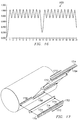
- FIG. 24 One simplified example of such a system is shown in Figure 24.
- two digital micromirror arrays 2400, 2402 as taught in U.S. Patent No. 5,061,049, "Spatial Light Modulator and Method," issued October 29, 1991, are illuminated by light sources 2404, 2406.
- Light reflected by the modulator arrays 2400, 2402 is focused on the printer drum 2408 by lenses 2410, 2412 to form two arrays of pixels 2414, 2416 which overlap over region 2422.
- each pixel may either be formed entirely by a single modulator array, or new breakpoint may be chosen for each row of the modulator array.
- the modulator arrays will be designed to clock the image data from one row of the modulator array to the next without the need to rewrite the image data into the modulator each row. In this case, using the same breakpoint for a row of pixels as it is passed from one row of the modulator array to the next is more efficient. If the data must be rewritten for each row of the modulator array, changing the breakpoint each time a given row of pixels is formed by another row of modulator elements will further reduce the visual artifacts.
- the disclosed invention may also be applied to systems that optically abut rows from a single modulator array.
- One example of such an optical system is taught by U.S. Patent No. 5,105,299, "Unfolded Optics for Multiple Row Deformable Mirror Device," issued April 14, 1992.
- a prism system 2502 may be used to optically shift the images 2504, 2506 from two parallel rows of modulator elements 2508, 2510 so that the images 2504, 2506 are co-linear and overlap.
- a mirror system 2602, as shown in Figure 26, may also be used to accomplish the same result.
- the modulators being aligned need not be arrays of individual elements.
- typical laser printers use a single laser source and a spinning mirror to scan across a row.
- An embodiment of the present invention, shown in Figure 27, could be used to allow the use of multiple laser sources 2700, 2702, or a single source and multiple light modulators, to simultaneously scan multiple laser beams 2708, 2710 across the photosensitive drum 2704.
- the two laser sources 2700, 2702 are reflecting of a shared spinning mirror 2706.
- the intensity from each laser beam would be reduced when the beam is impinging an area 2712 of the drum 2704 that is imaged by multiple laser beams 2708, 2710 so that the resultant image has the desired uniform intensity across all portions of the image.
- a large screen display system 2800 is comprised of an array of projection systems 2802 that project an image onto the rear of a display screen 2804.
- the display projected onto the screen 2804 consists of areas 2806 which are imaged by only one system, and an area 2808 shown in cross-hatch which is imaged by two or more of the projection systems 2802.
- Each individual projection system 2802 merely reduces the intensity of the display projected onto the shared areas 2808 so that sum of all the projection systems 2802 serves to evenly illuminate the entire display.
Landscapes
- Physics & Mathematics (AREA)
- Engineering & Computer Science (AREA)
- General Engineering & Computer Science (AREA)
- General Physics & Mathematics (AREA)
- Theoretical Computer Science (AREA)
- Optics & Photonics (AREA)
- Mathematical Physics (AREA)
- Mechanical Light Control Or Optical Switches (AREA)
- Printers Or Recording Devices Using Electromagnetic And Radiation Means (AREA)
- Facsimile Image Signal Circuits (AREA)
Applications Claiming Priority (2)
| Application Number | Priority Date | Filing Date | Title |
|---|---|---|---|
| US08/364,916 US5630027A (en) | 1994-12-28 | 1994-12-28 | Method and apparatus for compensating horizontal and vertical alignment errors in display systems |
| US364916 | 1994-12-28 |
Publications (2)
| Publication Number | Publication Date |
|---|---|
| EP0720119A2 true EP0720119A2 (de) | 1996-07-03 |
| EP0720119A3 EP0720119A3 (de) | 1997-12-10 |
Family
ID=23436661
Family Applications (1)
| Application Number | Title | Priority Date | Filing Date |
|---|---|---|---|
| EP95120025A Withdrawn EP0720119A3 (de) | 1994-12-28 | 1995-12-19 | Verfahren und Vorrichtung zur Bilderzeugung |
Country Status (5)
| Country | Link |
|---|---|
| US (2) | US5630027A (de) |
| EP (1) | EP0720119A3 (de) |
| JP (1) | JPH08258337A (de) |
| KR (1) | KR960024499A (de) |
| TW (1) | TW411703B (de) |
Cited By (5)
| Publication number | Priority date | Publication date | Assignee | Title |
|---|---|---|---|---|
| EP0866604A3 (de) * | 1997-03-19 | 2001-04-04 | Konica Corporation | Bildaufzeichnungsgerät mit mehreren Druckköpfen |
| EP0933925A3 (de) * | 1997-12-31 | 2002-06-26 | Texas Instruments Inc. | Fotobehandlung mit modulierten Lichtquellengittern |
| EP1528501A1 (de) * | 2003-10-29 | 2005-05-04 | Ricoh Company, Ltd. | Verfahren und Gerät zur optischen Wiedergabe eines Breitformatbildes mit einer Vielzahl von optischen Sendern |
| EP2057587A1 (de) * | 2006-10-03 | 2009-05-13 | Xaar Technology Limited | Drucker und druckverfahren |
| EP1452313A4 (de) * | 2001-12-03 | 2010-12-01 | Olympus Corp | Bildaufzeichnungsvorrichtung |
Families Citing this family (43)
| Publication number | Priority date | Publication date | Assignee | Title |
|---|---|---|---|---|
| US5630027A (en) * | 1994-12-28 | 1997-05-13 | Texas Instruments Incorporated | Method and apparatus for compensating horizontal and vertical alignment errors in display systems |
| JPH09226127A (ja) * | 1995-12-18 | 1997-09-02 | Canon Inc | 記録装置及びその方法、該装置を備えたファクシミリ装置 |
| JPH09292657A (ja) * | 1996-02-27 | 1997-11-11 | Fuji Photo Film Co Ltd | 画像露光装置並びにミラーアレイデバイスおよび液晶パネル |
| US5815303A (en) * | 1997-06-26 | 1998-09-29 | Xerox Corporation | Fault tolerant projective display having redundant light modulators |
| US6563601B1 (en) * | 1997-07-28 | 2003-05-13 | Canon Business Machines, Inc. | System for printing image data divided at a break point |
| US5870136A (en) * | 1997-12-05 | 1999-02-09 | The University Of North Carolina At Chapel Hill | Dynamic generation of imperceptible structured light for tracking and acquisition of three dimensional scene geometry and surface characteristics in interactive three dimensional computer graphics applications |
| US6503195B1 (en) | 1999-05-24 | 2003-01-07 | University Of North Carolina At Chapel Hill | Methods and systems for real-time structured light depth extraction and endoscope using real-time structured light depth extraction |
| US6643049B2 (en) * | 2001-02-01 | 2003-11-04 | Kodak Polychrome Graphics Llc | Compact imaging head and high speed multi-head laser imaging assembly and method |
| WO2002098145A1 (en) * | 2001-05-29 | 2002-12-05 | University Of Cincinnati | 3d display using micromirrors array |
| US20040238732A1 (en) * | 2001-10-19 | 2004-12-02 | Andrei State | Methods and systems for dynamic virtual convergence and head mountable display |
| AU2002251455A1 (en) * | 2002-03-12 | 2003-09-22 | Hewlett-Packard Indigo B.V. | Led print head printing |
| WO2003105289A2 (en) * | 2002-06-07 | 2003-12-18 | University Of North Carolina At Chapel Hill | Methods and systems for laser based real-time structured light depth extraction |
| EP1394732A1 (de) * | 2002-08-29 | 2004-03-03 | Dicon A/S | Verfahren zur Beleuchtung von mindestens zwei Beleuchtungspunkten |
| JP4315694B2 (ja) * | 2003-01-31 | 2009-08-19 | 富士フイルム株式会社 | 描画ヘッドユニット、描画装置及び描画方法 |
| JP2005199477A (ja) * | 2004-01-13 | 2005-07-28 | Fuji Photo Film Co Ltd | 発光装置 |
| US7182465B2 (en) * | 2004-02-25 | 2007-02-27 | The University Of North Carolina | Methods, systems, and computer program products for imperceptibly embedding structured light patterns in projected color images for display on planar and non-planar surfaces |
| US8152305B2 (en) * | 2004-07-16 | 2012-04-10 | The University Of North Carolina At Chapel Hill | Methods, systems, and computer program products for full spectrum projection |
| JP4802631B2 (ja) * | 2005-09-26 | 2011-10-26 | 富士ゼロックス株式会社 | 画像形成装置 |
| JP5020530B2 (ja) * | 2006-04-14 | 2012-09-05 | パナソニック株式会社 | 充電方法ならびに電池パックおよびその充電器 |
| US20110057930A1 (en) * | 2006-07-26 | 2011-03-10 | Inneroptic Technology Inc. | System and method of using high-speed, high-resolution depth extraction to provide three-dimensional imagery for endoscopy |
| WO2008017051A2 (en) | 2006-08-02 | 2008-02-07 | Inneroptic Technology Inc. | System and method of providing real-time dynamic imagery of a medical procedure site using multiple modalities |
| WO2009094646A2 (en) * | 2008-01-24 | 2009-07-30 | The University Of North Carolina At Chapel Hill | Methods, systems, and computer readable media for image guided ablation |
| US8340379B2 (en) | 2008-03-07 | 2012-12-25 | Inneroptic Technology, Inc. | Systems and methods for displaying guidance data based on updated deformable imaging data |
| US20090312629A1 (en) * | 2008-06-13 | 2009-12-17 | Inneroptic Technology Inc. | Correction of relative tracking errors based on a fiducial |
| JP4710941B2 (ja) * | 2008-09-10 | 2011-06-29 | 富士ゼロックス株式会社 | 画像形成装置 |
| US8554307B2 (en) | 2010-04-12 | 2013-10-08 | Inneroptic Technology, Inc. | Image annotation in image-guided medical procedures |
| US11464578B2 (en) | 2009-02-17 | 2022-10-11 | Inneroptic Technology, Inc. | Systems, methods, apparatuses, and computer-readable media for image management in image-guided medical procedures |
| US8641621B2 (en) | 2009-02-17 | 2014-02-04 | Inneroptic Technology, Inc. | Systems, methods, apparatuses, and computer-readable media for image management in image-guided medical procedures |
| US8690776B2 (en) | 2009-02-17 | 2014-04-08 | Inneroptic Technology, Inc. | Systems, methods, apparatuses, and computer-readable media for image guided surgery |
| ES2823456T3 (es) | 2009-06-25 | 2021-05-07 | Univ North Carolina Chapel Hill | Método y sistema para utilizar postes unidos a una superficie accionados para evaluar la reología de fluidos biológicos |
| WO2011014687A2 (en) * | 2009-07-31 | 2011-02-03 | Inneroptic Technology, Inc. | Dual-tube stereoscope |
| US20110082351A1 (en) * | 2009-10-07 | 2011-04-07 | Inneroptic Technology, Inc. | Representing measurement information during a medical procedure |
| US9282947B2 (en) | 2009-12-01 | 2016-03-15 | Inneroptic Technology, Inc. | Imager focusing based on intraoperative data |
| WO2013116240A1 (en) | 2012-01-30 | 2013-08-08 | Inneroptic Technology, Inc. | Multiple medical device guidance |
| US10314559B2 (en) | 2013-03-14 | 2019-06-11 | Inneroptic Technology, Inc. | Medical device guidance |
| US9901406B2 (en) | 2014-10-02 | 2018-02-27 | Inneroptic Technology, Inc. | Affected region display associated with a medical device |
| US10188467B2 (en) | 2014-12-12 | 2019-01-29 | Inneroptic Technology, Inc. | Surgical guidance intersection display |
| US9949700B2 (en) | 2015-07-22 | 2018-04-24 | Inneroptic Technology, Inc. | Medical device approaches |
| US9675319B1 (en) | 2016-02-17 | 2017-06-13 | Inneroptic Technology, Inc. | Loupe display |
| US10278778B2 (en) | 2016-10-27 | 2019-05-07 | Inneroptic Technology, Inc. | Medical device navigation using a virtual 3D space |
| US11259879B2 (en) | 2017-08-01 | 2022-03-01 | Inneroptic Technology, Inc. | Selective transparency to assist medical device navigation |
| US11484365B2 (en) | 2018-01-23 | 2022-11-01 | Inneroptic Technology, Inc. | Medical image guidance |
| CN110729790B (zh) * | 2019-10-28 | 2023-03-21 | Oppo广东移动通信有限公司 | 充电方法、装置、计算机设备与存储介质 |
Family Cites Families (19)
| Publication number | Priority date | Publication date | Assignee | Title |
|---|---|---|---|---|
| US4622561A (en) * | 1984-04-10 | 1986-11-11 | Ricoh Company, Ltd. | Image forming method for dot matrix printer |
| GB8427912D0 (en) * | 1984-11-05 | 1984-12-12 | Crosfield Electronics Ltd | Matching beam modulators |
| JPS63502142A (ja) * | 1986-01-22 | 1988-08-18 | ヒユ−ズ・エアクラフト・カンパニ− | バイポ−ラおよび複素数デ−タ処理用光アナログデ−タ処理システム |
| US4660052A (en) * | 1986-06-06 | 1987-04-21 | Mitsuhiro Kaiya | Heat-sensitive recording apparatus |
| JPH0288249A (ja) * | 1988-09-26 | 1990-03-28 | Hitachi Ltd | ドットプリンタ制御方式 |
| US5339090A (en) * | 1989-06-23 | 1994-08-16 | Northern Telecom Limited | Spatial light modulators |
| US5003323A (en) * | 1989-09-14 | 1991-03-26 | Seiko Instruments Inc. | Thermal line printer with an array of heating elements linearly arranged along the longitudinal inside edge portions of a plurality of longitudinally staggered head segments |
| US5260718A (en) * | 1990-01-24 | 1993-11-09 | Xerox Corporation | Liquid crystal shutter xerographic printer with offset configuration lamp aperture and copier/printer with optically aligned lamps, image bars, and lenses |
| US5079563A (en) * | 1990-02-20 | 1992-01-07 | Apple Computer, Inc. | Error reducing raster scan method |
| US5040876A (en) * | 1990-03-07 | 1991-08-20 | Bell Communications Research, Inc. | Liquid crystal light modulators with asymmetrical interfaces |
| EP0480437B1 (de) * | 1990-10-12 | 1997-01-02 | Fuji Photo Film Co., Ltd. | Abtast- und Beleuchtungsverfahren mit mehreren optischen Strahlen und Vorrichtung dazu |
| DE4110776A1 (de) * | 1991-03-28 | 1992-10-01 | Mannesmann Ag | Verfahren zum aufzeichnen von informationen |
| KR930002099A (ko) * | 1991-07-03 | 1993-02-22 | 이헌조 | 도트 프린터의 수직 정렬 오차 보상방법 |
| CA2087625C (en) * | 1992-01-23 | 2006-12-12 | William E. Nelson | Non-systolic time delay and integration printing |
| US5317445A (en) * | 1992-12-16 | 1994-05-31 | General Electric Company | Optical device with spatial light modulators for switching polarized light |
| DE9217340U1 (de) * | 1992-12-18 | 1993-02-18 | Nabinger, Erich, 6731 Frankenstein | Vorrichtung zum Befestigen einer Stützfeder |
| US5461411A (en) * | 1993-03-29 | 1995-10-24 | Texas Instruments Incorporated | Process and architecture for digital micromirror printer |
| US5461410A (en) * | 1993-03-29 | 1995-10-24 | Texas Instruments Incorporated | Gray scale printing using spatial light modulators |
| US5630027A (en) * | 1994-12-28 | 1997-05-13 | Texas Instruments Incorporated | Method and apparatus for compensating horizontal and vertical alignment errors in display systems |
-
1994
- 1994-12-28 US US08/364,916 patent/US5630027A/en not_active Expired - Lifetime
-
1995
- 1995-12-19 EP EP95120025A patent/EP0720119A3/de not_active Withdrawn
- 1995-12-27 TW TW084113909A patent/TW411703B/zh not_active IP Right Cessation
- 1995-12-27 JP JP34154495A patent/JPH08258337A/ja active Pending
- 1995-12-28 KR KR1019950061270A patent/KR960024499A/ko not_active Ceased
-
1998
- 1998-01-22 US US09/012,091 patent/US6137593A/en not_active Expired - Lifetime
Cited By (6)
| Publication number | Priority date | Publication date | Assignee | Title |
|---|---|---|---|---|
| EP0866604A3 (de) * | 1997-03-19 | 2001-04-04 | Konica Corporation | Bildaufzeichnungsgerät mit mehreren Druckköpfen |
| EP0933925A3 (de) * | 1997-12-31 | 2002-06-26 | Texas Instruments Inc. | Fotobehandlung mit modulierten Lichtquellengittern |
| EP1452313A4 (de) * | 2001-12-03 | 2010-12-01 | Olympus Corp | Bildaufzeichnungsvorrichtung |
| EP1528501A1 (de) * | 2003-10-29 | 2005-05-04 | Ricoh Company, Ltd. | Verfahren und Gerät zur optischen Wiedergabe eines Breitformatbildes mit einer Vielzahl von optischen Sendern |
| US7248277B2 (en) | 2003-10-29 | 2007-07-24 | Ricoh Company, Ltd. | Method and apparatus for optical writing capable of writing a wide format image using a plurality of light emitting devices |
| EP2057587A1 (de) * | 2006-10-03 | 2009-05-13 | Xaar Technology Limited | Drucker und druckverfahren |
Also Published As
| Publication number | Publication date |
|---|---|
| EP0720119A3 (de) | 1997-12-10 |
| US6137593A (en) | 2000-10-24 |
| JPH08258337A (ja) | 1996-10-08 |
| KR960024499A (ko) | 1996-07-20 |
| US5630027A (en) | 1997-05-13 |
| TW411703B (en) | 2000-11-11 |
Similar Documents
| Publication | Publication Date | Title |
|---|---|---|
| US6137593A (en) | Method of compensating horizontal and vertical alignment errors in display systems | |
| US5825400A (en) | Method and apparatus for ameliorating the effects of misalignment between two or more imaging elements | |
| JP3165208B2 (ja) | ゼログラフィックシステム及びグレイスケール生成方法 | |
| EP0636997B1 (de) | Räumliche Lichtmodulation | |
| KR100318033B1 (ko) | 공간광변조기들을사용한그레이스케일프린팅 | |
| US5103334A (en) | Resolution improvement in flying spot scanner | |
| KR100296067B1 (ko) | 디지탈마이크로미러프린터를위한변조방법 | |
| JP2583717B2 (ja) | 微細位置指定可能な表示装置 | |
| CN100428066C (zh) | 成像设备 | |
| JP2584111B2 (ja) | 画素位置を修正する方法 | |
| JPH0362154B2 (de) | ||
| US4963900A (en) | Multiple laser beam scanning optics | |
| EP0246457A2 (de) | Kompensation beim Drucken feiner Striche | |
| EP1293348B1 (de) | Bildaufzeichnungsverfahren und -Vorrichtung | |
| US5684620A (en) | High resolution imaging system and method of imaging using the same | |
| EP0709802A2 (de) | Überlappende optische Abtastung | |
| EP0658857B1 (de) | Bildaufzeichnungsgerät | |
| US6700597B2 (en) | Two dimensional scanning image recording method and image recording apparatus with two-dimensionally disposed light source elements | |
| US6731321B2 (en) | Image recording method and image recording apparatus | |
| JPH05138946A (ja) | 画像形成装置 | |
| JP3019598B2 (ja) | 画像記録装置 | |
| JP3143489B2 (ja) | 画像形成装置及び方法 | |
| JPH0862911A (ja) | 空間光変調法及び装置 | |
| JPH01179176A (ja) | 画像形成装置 | |
| JPH0577485A (ja) | ラスタプロツタ装置 |
Legal Events
| Date | Code | Title | Description |
|---|---|---|---|
| PUAI | Public reference made under article 153(3) epc to a published international application that has entered the european phase |
Free format text: ORIGINAL CODE: 0009012 |
|
| AK | Designated contracting states |
Kind code of ref document: A2 Designated state(s): DE FR GB IT NL |
|
| PUAL | Search report despatched |
Free format text: ORIGINAL CODE: 0009013 |
|
| AK | Designated contracting states |
Kind code of ref document: A3 Designated state(s): DE FR GB IT NL |
|
| 17P | Request for examination filed |
Effective date: 19980514 |
|
| 17Q | First examination report despatched |
Effective date: 20001219 |
|
| STAA | Information on the status of an ep patent application or granted ep patent |
Free format text: STATUS: THE APPLICATION IS DEEMED TO BE WITHDRAWN |
|
| 18D | Application deemed to be withdrawn |
Effective date: 20010502 |