EP0809360A2 - Circuit intégré avec un transistor à collecteur ouvert du type NPN - Google Patents
Circuit intégré avec un transistor à collecteur ouvert du type NPN Download PDFInfo
- Publication number
- EP0809360A2 EP0809360A2 EP97107428A EP97107428A EP0809360A2 EP 0809360 A2 EP0809360 A2 EP 0809360A2 EP 97107428 A EP97107428 A EP 97107428A EP 97107428 A EP97107428 A EP 97107428A EP 0809360 A2 EP0809360 A2 EP 0809360A2
- Authority
- EP
- European Patent Office
- Prior art keywords
- collector
- transistor
- base
- control transistor
- current
- Prior art date
- Legal status (The legal status is an assumption and is not a legal conclusion. Google has not performed a legal analysis and makes no representation as to the accuracy of the status listed.)
- Granted
Links
Images
Classifications
-
- H—ELECTRICITY
- H03—ELECTRONIC CIRCUITRY
- H03K—PULSE TECHNIQUE
- H03K17/00—Electronic switching or gating, i.e. not by contact-making and –breaking
- H03K17/16—Modifications for eliminating interference voltages or currents
-
- H—ELECTRICITY
- H03—ELECTRONIC CIRCUITRY
- H03K—PULSE TECHNIQUE
- H03K17/00—Electronic switching or gating, i.e. not by contact-making and –breaking
- H03K17/08—Modifications for protecting switching circuit against overcurrent or overvoltage
- H03K17/082—Modifications for protecting switching circuit against overcurrent or overvoltage by feedback from the output to the control circuit
- H03K17/0826—Modifications for protecting switching circuit against overcurrent or overvoltage by feedback from the output to the control circuit in bipolar transistor switches
-
- H—ELECTRICITY
- H10—SEMICONDUCTOR DEVICES; ELECTRIC SOLID-STATE DEVICES NOT OTHERWISE PROVIDED FOR
- H10D—INORGANIC ELECTRIC SEMICONDUCTOR DEVICES
- H10D84/00—Integrated devices formed in or on semiconductor substrates that comprise only semiconducting layers, e.g. on Si wafers or on GaAs-on-Si wafers
- H10D84/60—Integrated devices formed in or on semiconductor substrates that comprise only semiconducting layers, e.g. on Si wafers or on GaAs-on-Si wafers characterised by the integration of at least one component covered by groups H10D10/00 or H10D18/00, e.g. integration of BJTs
- H10D84/645—Combinations of only lateral BJTs
Definitions
- the invention relates to a circuit arrangement according to the preamble of patent claim 1.
- Such a circuit arrangement is from the Tietze / Schenk reference: Semiconductor circuit technology ", Springer-Verlag Berlin, 1978, page 161.
- the circuit arrangement described there has an npn transistor as the output stage, the emitter of which is connected to a ground connection and the collector of which is connected to an open collector output of the circuit arrangement
- the open collector output can be connected to open collector outputs of further circuit arrangements and, via a resistor, to a supply connection, to which a supply voltage is supplied.
- the invention is therefore based on the object of specifying a circuit arrangement according to the preamble of patent claim 1 is simple to produce and has improved properties with regard to parasitic effects.
- the collector of the open collector transistor is connected via a, preferably low-resistance, collector resistor to the open collector output of the circuit arrangement, at which the output voltage is applied, and via a parasitic diode to the ground connection of the circuit arrangement, to which a reference potential is present , connected.
- the parasitic diode is formed from the collector region of the open collector transistor and from a p-doped separation zone surrounding this collector region, which is provided for isolating the open collector transistor from further circuit parts of the circuit arrangement. It is switched in the reverse direction at positive voltage values of the output voltage, i. H. it is connected on the cathode side to the collector of the open collector transistor and on the anode side to the ground connection of the circuit arrangement.
- the open collector transistor can be controlled by a base current, which is generated by a base current source connected to the base of the open collector transistor. It is operated with positive voltage values of the output voltage in the forward direction and with negative voltage values of the output voltage in the reverse direction, whereby if the voltage values of the output voltage fall below a negative threshold voltage value, it is switched into an inverse conductive state by the base current, in which a voltage drops across the collector resistor due to of a collector current of the open collector transistor then flowing through the collector resistance is so great that the parasitic diode remains switched in the reverse direction.
- a base current which is generated by a base current source connected to the base of the open collector transistor. It is operated with positive voltage values of the output voltage in the forward direction and with negative voltage values of the output voltage in the reverse direction, whereby if the voltage values of the output voltage fall below a negative threshold voltage value, it is switched into an inverse conductive state by the base current, in which a voltage drops across the collector resistor due to of a collector current of the open collector transistor
- the base current source preferably has a control current source connected to the base of the open collector transistor, which can be switched via a switching signal applied to a switching input of the control current source.
- the open collector transistor is switched on and off at positive voltage values at the open collector output by switching the control current source can be switched off, ie switchable between a low-resistance state and a higher-resistance state.
- the base current source has a first control transistor and a first quiescent current source connected to its collector.
- the first control transistor and the open collector transistor are connected as a current mirror arrangement to the first quiescent current source as a reference current source.
- the base current source has a second control transistor for the low-resistance coupling of the base current, the base of which is connected to the collector of the first control transistor, the emitter of which is connected to the base of the first control transistor and the collector of which is connected to a supply connection of the circuit arrangement to which a supply voltage is applied is.
- the second control transistor it preferably has a third control transistor which is connected to the second control transistor as a Darlington stage.
- the comparator stage preferably has two comparator inputs, each connected to one connection of the collector resistor, and a comparator output, at which the limit signal is present. This limit signal is fed to a control input of the base current source, which is connected to the comparator output of the comparator stage and via which the base current can be controlled.
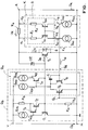
- the collector of the open collector transistor T 0 is connected via the collector resistor R 0 , at which the voltage U R drops, to the open collector output A of the circuit arrangement, at which the output voltage U A is present, which
- the emitter of the open collector transistor T 0 is connected to the ground terminal M of the circuit arrangement, to which a reference potential is present, and the base of the open collector transistor T 0 is connected to the base current source Q B , which supplies the base current I B for controlling the open Collector transistor T 0 supplies, connected.
- the Zener diode DZ which is connected on the cathode side to the collector and on the anode side to the base of the open collector transistor T 0 , serves to protect the open collector transistor T 0 against excessive collector-emitter voltages.
- the entire circuit arrangement is integrated on a semiconductor substrate of an integrated circuit, it also being possible for further circuit parts, not shown in the figure, to be integrated on the same semiconductor substrate.
- the collector of the open collector transistor T 0 is surrounded by a p-doped and connected to the ground terminal M separation zone and isolated by this from further n-doped semiconductor regions.
- the separation zone and the collector region of the open collector transistor T 0 form the parasitic diode D indicated by dashed lines.
- the base current source Q B comprises the control current source Q S , the first quiescent current source Q R1 , the first control transistor T 1 , the second control transistor T 2 , the third control transistor T 3 , the limiting resistor R B and the bleeder resistor R A.
- the emitter of the first control transistor T 1 is connected to the Ground terminal M connected, the collector of the first control transistor T 1 is connected to the base of the third control transistor T 3 and via the first quiescent current source Q R1 to the supply terminal V, to which the supply voltage U B is supplied, the collectors of the second and the third control transistor T 2 and T 3 are connected to the supply terminal V via the limiting resistor R B and the base of the first control transistor T 1 is connected to the emitter of the second control transistor T 2 , to the base of the open collector transistor T 0 and via the bleeder resistor R A connected to the ground terminal M.
- the bleeder resistor R A serves to set a defined potential at the base of the first control transistor T 1 and the limiting resistor R B serves to limit the current flowing through the second control transistor T 2 .
- the control current source Q S includes the second quiescent current source Q R2 , the third quiescent current source Q R3 , the fourth control transistor T 4 , the fifth control transistor T 5 , the sixth control transistor T 6 and the capacitor C.
- the emitter of the fourth control transistor T 4 with the Base of the open collector transistor T 0 connected the collector of the fourth control transistor T 4 connected to the supply terminal V via the second quiescent current source Q R2 , the base of the fourth control transistor T 4 to the collectors of the fifth and sixth control transistors T 5 and T 6 , connected to the control input Q 2 of the base current source Q B via the capacitor C and to the supply terminal V via the third quiescent current source Q R3 .
- the base of the fifth control transistor T S is connected to the switching terminal Q 1 of the control current source Q S , at which a voltage is present as a switching signal U S for switching the control current source Q S , and the base of the sixth control transistor T 6 is connected to the control input Q 2 Base current source Q B , which simultaneously forms a control input of the control current source Q S and at which a current is present as a limiting signal I G.
- the comparator stage K comprises the two comparator resistors R 1 , R 2 , the two comparator transistors T K1 , T K2 and the two constant current sources Q K1 , Q K2 .
- the bases of the comparator transistors T K1 , T K2 are connected to the collector one of the comparator transistor T K1 and one constant current source Q K1 to the ground terminal M and the collector of the other comparator transistor T K2 is connected to the comparator output K 3 , which is connected to the control input Q 2 of the base current source Q B , and via the other constant current source Q K2
- the two comparator resistors R 1 , R 2 and the two comparator transistors T K1 , T K2 therefore form a current mirror arrangement S with the collector of one comparator transistor T K1 as a reference current input S R , at which the current I K1 of the one constant current source Q K1 is present as a reference current, and with the collector of the other comparator transistor T K2 as a mirror current output S A , at which the mirror current I S is present.
- the control transistors T 1 , T 2 , T 3 , T 4 , T 5 , T 6 and the open collector transistor T 0 are designed as npn transistors and the comparator transistors T K1 , T K2 as pnp transistors.
- the open collector transistor T 0 is therefore operated in the forward direction at positive voltage values of the output voltage U A , ie at potentials at the open terminal output A that are positive with respect to the reference potential at the ground connection M. It is then switched on at a low level of the switching signal U S corresponding to the reference potential and switched off at a high level of the switching signal U S , for example corresponding to the supply voltage U B.
- the fifth control transistor T 5 At the high level of the switching signal U S of the fifth control transistor T 5 is conductive, and thus executes all of the third quiescent current source Q R3 deliverable current I R3 to the ground terminal from M.
- the fourth control transistor T 4 and the control current source Q S are consequently blocked and therefore make no contribution to the base current I B.
- the base current I B is not equal to zero, since the control transistors T 1 , T 2 and T 3 and the open collector transistor T 0 act as a current mirror arrangement with which the current I R1 of the first quiescent current source Q R1 as the collector current I K des Open collector transistor T 0 is mirrored to open collector output A.
- the mirror ratio - the ratio of the collector current I K of the open collector transistor T 0 and the current I R1 of the first quiescent current source Q R1 - is set to a value of, for example, 20 by the ratio of the emitter area of the open collector transistor T 0 and the emitter area of the first control transistor T 1 .
- the collector current I K is then 1.5 mA. This is the minimum collector current I K flowing through the open collector transistor T 0 , ie the open collector transistor T 0 is not completely blocking in the switched-off state, but is only in a higher-resistance state than in the switched-on state.
- the fifth control transistor T 5 When the switching signal U S is low, the fifth control transistor T 5 is blocked, so that the current I R3 of the third quiescent current source Q R3 is supplied to the base of the fourth control transistor T 4 . This is therefore conductive and consequently conducts the current I R2 of the second quiescent current source Q R2 , which is, for example, about 3 mA, to the base of the open collector transistor T 0 , which is thereby switched on, ie switched to a low-resistance state.
- part of the current I R3 of the third quiescent current source Q R3 is derived via the sixth control transistor T 6 to the ground terminal M, so that only part of the current available from the second quiescent current source Q R2 Current I R2 can be supplied via the fourth control transistor T 4 to the base of the open collector transistor T 0 , ie the base current I B and consequently also the collector current I K are reduced by the limiting signal I G.
- the resistance values of the collector resistor R 0 and the comparator resistors R 1 , R 2 are selected such that the current I K1 of the one constant current source Q K1 and the mirror current I S of the current mirror arrangement S are the same when the collector current I K of the open collector Transistor T 0 is equal to a threshold current value of 80 mA, for example.
- a resistance value of the collector resistance R 0 of, for example, 3 ⁇ the one comparator resistance R 1 is for example 2 k ⁇ and the other comparator resistance R 2 is 11.6 k ⁇ .
- the two constant current sources Q K1 , Q K2 only supply small currents I K1 , I K2 , which are the same and, for example, each amount to 25 ⁇ A, so that the circuit arrangement is only slightly loaded by the comparator stage K. If the current value of the collector current I K exceeds the threshold current value, the voltage drop between the open collector output A and the emitter of the one comparator transistor T K1 is greater than the voltage drop between the open collector output A and the emitter of the other comparator transistor T K2 . Consequently, the mirror current I S is also greater than the current I K1 of the one constant current source Q K1 .
- the portion of the mirror current I S which exceeds the current I K2 of the second constant current source Q K2 is then fed to the control input Q 2 of the base current source Q B as the limiting signal I G.
- the collector current I K is then limited by reducing the base current I B to a current value below the threshold current value.
- the capacitor C prevents the circuit arrangement from being excited to oscillate as a result.
- the open collector transistor T 0 is operated in the reverse direction, ie inversely, at negative voltage values of the output voltage U A. It is switched into an inversely conductive state at voltage values of the output voltage U A which fall below a negative threshold voltage which is less than the reference potential by a diode forward voltage (0.7 V).
- the collector current I K then flows from the collector of the open collector transistor T 0 through the collector resistor R 0 to the open collector output A, so that it is the open collector transistor T 0 and the control transistors T 1 , T 2 , T 3 no longer act as a current mirror arrangement.
- the parasitic diode D Since the parasitic diode D is supposed to be blocking, the voltage U R dropping across the collector resistor R 0 must be so great that the open collector transistor T 0 has a potential at the collector which represents the reference potential at the ground connection M and consequently also the potential at the separation zone is less than a diode forward voltage.
- the collector current I K since the voltage U R depends on it, must be designed to be correspondingly large.
- the parasitic diode D is then switched in the reverse direction for all voltage values of the output voltage U A which lie within a permissible value range of, for example, -1 V to 29 V. The smallest value of the permissible value range is predetermined by the collector current I K and the collector resistance R 0 .
- the collector resistance R 0 must not be too large. Therefore, the collector current I K must be designed to be correspondingly large by choosing a sufficiently large base current I B.
- the current gain of the open collector transistor T 0 is significantly smaller when operating in the reverse direction than when operating in the forward direction. Accordingly, for example, to generate a collector current I K of -200 mA, a base current I B of approx. 20 mA is required.
Landscapes
- Bipolar Integrated Circuits (AREA)
- Amplifiers (AREA)
- Electronic Switches (AREA)
- Power Conversion In General (AREA)
Applications Claiming Priority (2)
| Application Number | Priority Date | Filing Date | Title |
|---|---|---|---|
| DE19620564 | 1996-05-22 | ||
| DE19620564A DE19620564C1 (de) | 1996-05-22 | 1996-05-22 | Integrierte Schaltungsanordnung mit einem als npn-Transistor ausgebildeten Open-Collector-Transistor |
Publications (3)
| Publication Number | Publication Date |
|---|---|
| EP0809360A2 true EP0809360A2 (fr) | 1997-11-26 |
| EP0809360A3 EP0809360A3 (fr) | 1998-07-15 |
| EP0809360B1 EP0809360B1 (fr) | 2000-08-02 |
Family
ID=7794983
Family Applications (1)
| Application Number | Title | Priority Date | Filing Date |
|---|---|---|---|
| EP97107428A Expired - Lifetime EP0809360B1 (fr) | 1996-05-22 | 1997-05-06 | Circuit intégré avec un transistor à collecteur ouvert du type NPN |
Country Status (5)
| Country | Link |
|---|---|
| US (1) | US5973513A (fr) |
| EP (1) | EP0809360B1 (fr) |
| JP (1) | JPH10107604A (fr) |
| DE (2) | DE19620564C1 (fr) |
| ES (1) | ES2149529T3 (fr) |
Families Citing this family (1)
| Publication number | Priority date | Publication date | Assignee | Title |
|---|---|---|---|---|
| FR3039905B1 (fr) | 2015-08-07 | 2019-01-25 | STMicroelectronics (Alps) SAS | Source de tension |
Family Cites Families (6)
| Publication number | Priority date | Publication date | Assignee | Title |
|---|---|---|---|---|
| JPS57121321A (en) * | 1981-01-21 | 1982-07-28 | Yamatake Honeywell Co Ltd | Open collector output type digital circuit |
| DE3237141C1 (de) * | 1982-10-07 | 1983-07-28 | Danfoss A/S, 6430 Nordborg | Steuervorrichtung für einen Schalttransistor |
| EP0190925B1 (fr) * | 1985-02-08 | 1993-12-29 | Kabushiki Kaisha Toshiba | Circuit de protection pour un transistor bipolaire à grille isolée |
| GB2204445B (en) * | 1987-03-06 | 1991-04-24 | Texas Instruments Ltd | Semiconductor switch |
| US4965466A (en) * | 1989-07-19 | 1990-10-23 | Motorola, Inc. | Substrate injection clamp |
| JPH03270407A (ja) * | 1990-03-20 | 1991-12-02 | Fujitsu Ltd | 半導体集積回路 |
-
1996
- 1996-05-22 DE DE19620564A patent/DE19620564C1/de not_active Expired - Fee Related
-
1997
- 1997-05-06 ES ES97107428T patent/ES2149529T3/es not_active Expired - Lifetime
- 1997-05-06 EP EP97107428A patent/EP0809360B1/fr not_active Expired - Lifetime
- 1997-05-06 DE DE59702101T patent/DE59702101D1/de not_active Expired - Lifetime
- 1997-05-07 US US08/852,473 patent/US5973513A/en not_active Expired - Lifetime
- 1997-05-16 JP JP9161767A patent/JPH10107604A/ja active Pending
Also Published As
| Publication number | Publication date |
|---|---|
| US5973513A (en) | 1999-10-26 |
| DE19620564C1 (de) | 1997-07-10 |
| EP0809360B1 (fr) | 2000-08-02 |
| JPH10107604A (ja) | 1998-04-24 |
| DE59702101D1 (de) | 2000-09-07 |
| ES2149529T3 (es) | 2000-11-01 |
| EP0809360A3 (fr) | 1998-07-15 |
Similar Documents
| Publication | Publication Date | Title |
|---|---|---|
| DE1812292C3 (de) | Schaltungsanordnung zur Verstärkungsregelung | |
| EP0093996B1 (fr) | Circuit pour la conversion de niveau | |
| DE2727537A1 (de) | Schwellwert-detektor | |
| WO1997033365A1 (fr) | Amplificateur operationnel | |
| DE60130696T2 (de) | Vorspannungsschaltung für einen Feldeffekttransistor | |
| DE3537920A1 (de) | Elektronischer spannungsstabilisator mit schutz gegen uebergangs-ueberspannungen, deren polaritaet entgegengesetzt zur polaritaet des generators ist, insbesondere fuer die verwendung in kraftfahrzeugen | |
| EP0106088B1 (fr) | Amplificateur à semi-conducteurs en circuit intégré | |
| EP0334447B1 (fr) | Circuit déclencheur de Schmitt | |
| EP1033809B1 (fr) | Amplificateur différentiel | |
| DE1537185B2 (de) | Amplitudenfilter | |
| DE2924171C2 (fr) | ||
| DE2853581C2 (de) | Emitterfolgerschaltung | |
| DE2506034A1 (de) | Schaltungsanordnung zum elektronischen durchschalten einer wechselspannung | |
| DE3210661A1 (de) | Verstaerker | |
| DE3615383A1 (de) | Eine schaltung zur verschiebung des eingangspegels eines digital-analog-wandlers | |
| EP0809360B1 (fr) | Circuit intégré avec un transistor à collecteur ouvert du type NPN | |
| DE69024711T2 (de) | Verstärkerschaltung | |
| DE2056078C3 (de) | Rückgekoppelter Verriegelungsschalter | |
| WO1993006541A1 (fr) | Dispositif de generation de tensions intermediaires | |
| DE2820416A1 (de) | Schalterkeis | |
| DE2148880C2 (de) | Stromquelle in integrierter Schaltungstechnik | |
| EP0541164A1 (fr) | Amplificateur | |
| EP0676846B1 (fr) | Commutateur réalisé avec transistor bipolaire comme premier élément de commutation | |
| EP0185377B1 (fr) | Circuit de signalisation | |
| DE3615513A1 (de) | Digital-analog-wandler fuer niedrige spannungswerte |
Legal Events
| Date | Code | Title | Description |
|---|---|---|---|
| PUAI | Public reference made under article 153(3) epc to a published international application that has entered the european phase |
Free format text: ORIGINAL CODE: 0009012 |
|
| AK | Designated contracting states |
Kind code of ref document: A2 Designated state(s): DE ES FR GB IT SE |
|
| PUAL | Search report despatched |
Free format text: ORIGINAL CODE: 0009013 |
|
| AK | Designated contracting states |
Kind code of ref document: A3 Designated state(s): DE ES FR GB IT SE |
|
| 17P | Request for examination filed |
Effective date: 19980808 |
|
| RAP1 | Party data changed (applicant data changed or rights of an application transferred) |
Owner name: TEMIC SEMICONDUCTOR GMBH |
|
| GRAG | Despatch of communication of intention to grant |
Free format text: ORIGINAL CODE: EPIDOS AGRA |
|
| GRAG | Despatch of communication of intention to grant |
Free format text: ORIGINAL CODE: EPIDOS AGRA |
|
| GRAH | Despatch of communication of intention to grant a patent |
Free format text: ORIGINAL CODE: EPIDOS IGRA |
|
| 17Q | First examination report despatched |
Effective date: 19991109 |
|
| GRAH | Despatch of communication of intention to grant a patent |
Free format text: ORIGINAL CODE: EPIDOS IGRA |
|
| ITF | It: translation for a ep patent filed | ||
| GRAA | (expected) grant |
Free format text: ORIGINAL CODE: 0009210 |
|
| AK | Designated contracting states |
Kind code of ref document: B1 Designated state(s): DE ES FR GB IT SE |
|
| REF | Corresponds to: |
Ref document number: 59702101 Country of ref document: DE Date of ref document: 20000907 |
|
| GBT | Gb: translation of ep patent filed (gb section 77(6)(a)/1977) |
Effective date: 20000925 |
|
| ET | Fr: translation filed | ||
| REG | Reference to a national code |
Ref country code: ES Ref legal event code: FG2A Ref document number: 2149529 Country of ref document: ES Kind code of ref document: T3 |
|
| RAP2 | Party data changed (patent owner data changed or rights of a patent transferred) |
Owner name: ATMEL GERMANY GMBH |
|
| PLBE | No opposition filed within time limit |
Free format text: ORIGINAL CODE: 0009261 |
|
| STAA | Information on the status of an ep patent application or granted ep patent |
Free format text: STATUS: NO OPPOSITION FILED WITHIN TIME LIMIT |
|
| 26N | No opposition filed | ||
| REG | Reference to a national code |
Ref country code: GB Ref legal event code: IF02 |
|
| PGFP | Annual fee paid to national office [announced via postgrant information from national office to epo] |
Ref country code: ES Payment date: 20080529 Year of fee payment: 12 |
|
| PGFP | Annual fee paid to national office [announced via postgrant information from national office to epo] |
Ref country code: IT Payment date: 20080524 Year of fee payment: 12 |
|
| PGFP | Annual fee paid to national office [announced via postgrant information from national office to epo] |
Ref country code: SE Payment date: 20080513 Year of fee payment: 12 |
|
| PGFP | Annual fee paid to national office [announced via postgrant information from national office to epo] |
Ref country code: GB Payment date: 20080522 Year of fee payment: 12 |
|
| GBPC | Gb: european patent ceased through non-payment of renewal fee |
Effective date: 20090506 |
|
| REG | Reference to a national code |
Ref country code: FR Ref legal event code: ST Effective date: 20100129 |
|
| PG25 | Lapsed in a contracting state [announced via postgrant information from national office to epo] |
Ref country code: FR Free format text: LAPSE BECAUSE OF NON-PAYMENT OF DUE FEES Effective date: 20090602 |
|
| PGFP | Annual fee paid to national office [announced via postgrant information from national office to epo] |
Ref country code: FR Payment date: 20080526 Year of fee payment: 12 |
|
| PG25 | Lapsed in a contracting state [announced via postgrant information from national office to epo] |
Ref country code: GB Free format text: LAPSE BECAUSE OF NON-PAYMENT OF DUE FEES Effective date: 20090506 |
|
| REG | Reference to a national code |
Ref country code: ES Ref legal event code: FD2A Effective date: 20090507 |
|
| PG25 | Lapsed in a contracting state [announced via postgrant information from national office to epo] |
Ref country code: ES Free format text: LAPSE BECAUSE OF NON-PAYMENT OF DUE FEES Effective date: 20090507 |
|
| PG25 | Lapsed in a contracting state [announced via postgrant information from national office to epo] |
Ref country code: IT Free format text: LAPSE BECAUSE OF NON-PAYMENT OF DUE FEES Effective date: 20090506 |
|
| PG25 | Lapsed in a contracting state [announced via postgrant information from national office to epo] |
Ref country code: SE Free format text: LAPSE BECAUSE OF NON-PAYMENT OF DUE FEES Effective date: 20090507 |
|
| PGFP | Annual fee paid to national office [announced via postgrant information from national office to epo] |
Ref country code: DE Payment date: 20120529 Year of fee payment: 16 |
|
| PG25 | Lapsed in a contracting state [announced via postgrant information from national office to epo] |
Ref country code: DE Free format text: LAPSE BECAUSE OF NON-PAYMENT OF DUE FEES Effective date: 20131203 |
|
| REG | Reference to a national code |
Ref country code: DE Ref legal event code: R119 Ref document number: 59702101 Country of ref document: DE Effective date: 20131203 |