EP0809360A2 - Integrated circuit with an NPN-type open collector transistor - Google Patents
Integrated circuit with an NPN-type open collector transistor Download PDFInfo
- Publication number
- EP0809360A2 EP0809360A2 EP97107428A EP97107428A EP0809360A2 EP 0809360 A2 EP0809360 A2 EP 0809360A2 EP 97107428 A EP97107428 A EP 97107428A EP 97107428 A EP97107428 A EP 97107428A EP 0809360 A2 EP0809360 A2 EP 0809360A2
- Authority
- EP
- European Patent Office
- Prior art keywords
- collector
- transistor
- base
- control transistor
- current
- Prior art date
- Legal status (The legal status is an assumption and is not a legal conclusion. Google has not performed a legal analysis and makes no representation as to the accuracy of the status listed.)
- Granted
Links
Images
Classifications
-
- H—ELECTRICITY
- H03—ELECTRONIC CIRCUITRY
- H03K—PULSE TECHNIQUE
- H03K17/00—Electronic switching or gating, i.e. not by contact-making and –breaking
- H03K17/16—Modifications for eliminating interference voltages or currents
-
- H—ELECTRICITY
- H03—ELECTRONIC CIRCUITRY
- H03K—PULSE TECHNIQUE
- H03K17/00—Electronic switching or gating, i.e. not by contact-making and –breaking
- H03K17/08—Modifications for protecting switching circuit against overcurrent or overvoltage
- H03K17/082—Modifications for protecting switching circuit against overcurrent or overvoltage by feedback from the output to the control circuit
- H03K17/0826—Modifications for protecting switching circuit against overcurrent or overvoltage by feedback from the output to the control circuit in bipolar transistor switches
-
- H—ELECTRICITY
- H10—SEMICONDUCTOR DEVICES; ELECTRIC SOLID-STATE DEVICES NOT OTHERWISE PROVIDED FOR
- H10D—INORGANIC ELECTRIC SEMICONDUCTOR DEVICES
- H10D84/00—Integrated devices formed in or on semiconductor substrates that comprise only semiconducting layers, e.g. on Si wafers or on GaAs-on-Si wafers
- H10D84/60—Integrated devices formed in or on semiconductor substrates that comprise only semiconducting layers, e.g. on Si wafers or on GaAs-on-Si wafers characterised by the integration of at least one component covered by groups H10D10/00 or H10D18/00, e.g. integration of BJTs
- H10D84/645—Combinations of only lateral BJTs
Definitions
- the invention relates to a circuit arrangement according to the preamble of patent claim 1.
- Such a circuit arrangement is from the Tietze / Schenk reference: Semiconductor circuit technology ", Springer-Verlag Berlin, 1978, page 161.
- the circuit arrangement described there has an npn transistor as the output stage, the emitter of which is connected to a ground connection and the collector of which is connected to an open collector output of the circuit arrangement
- the open collector output can be connected to open collector outputs of further circuit arrangements and, via a resistor, to a supply connection, to which a supply voltage is supplied.
- the invention is therefore based on the object of specifying a circuit arrangement according to the preamble of patent claim 1 is simple to produce and has improved properties with regard to parasitic effects.
- the collector of the open collector transistor is connected via a, preferably low-resistance, collector resistor to the open collector output of the circuit arrangement, at which the output voltage is applied, and via a parasitic diode to the ground connection of the circuit arrangement, to which a reference potential is present , connected.
- the parasitic diode is formed from the collector region of the open collector transistor and from a p-doped separation zone surrounding this collector region, which is provided for isolating the open collector transistor from further circuit parts of the circuit arrangement. It is switched in the reverse direction at positive voltage values of the output voltage, i. H. it is connected on the cathode side to the collector of the open collector transistor and on the anode side to the ground connection of the circuit arrangement.
- the open collector transistor can be controlled by a base current, which is generated by a base current source connected to the base of the open collector transistor. It is operated with positive voltage values of the output voltage in the forward direction and with negative voltage values of the output voltage in the reverse direction, whereby if the voltage values of the output voltage fall below a negative threshold voltage value, it is switched into an inverse conductive state by the base current, in which a voltage drops across the collector resistor due to of a collector current of the open collector transistor then flowing through the collector resistance is so great that the parasitic diode remains switched in the reverse direction.
- a base current which is generated by a base current source connected to the base of the open collector transistor. It is operated with positive voltage values of the output voltage in the forward direction and with negative voltage values of the output voltage in the reverse direction, whereby if the voltage values of the output voltage fall below a negative threshold voltage value, it is switched into an inverse conductive state by the base current, in which a voltage drops across the collector resistor due to of a collector current of the open collector transistor
- the base current source preferably has a control current source connected to the base of the open collector transistor, which can be switched via a switching signal applied to a switching input of the control current source.
- the open collector transistor is switched on and off at positive voltage values at the open collector output by switching the control current source can be switched off, ie switchable between a low-resistance state and a higher-resistance state.
- the base current source has a first control transistor and a first quiescent current source connected to its collector.
- the first control transistor and the open collector transistor are connected as a current mirror arrangement to the first quiescent current source as a reference current source.
- the base current source has a second control transistor for the low-resistance coupling of the base current, the base of which is connected to the collector of the first control transistor, the emitter of which is connected to the base of the first control transistor and the collector of which is connected to a supply connection of the circuit arrangement to which a supply voltage is applied is.
- the second control transistor it preferably has a third control transistor which is connected to the second control transistor as a Darlington stage.
- the comparator stage preferably has two comparator inputs, each connected to one connection of the collector resistor, and a comparator output, at which the limit signal is present. This limit signal is fed to a control input of the base current source, which is connected to the comparator output of the comparator stage and via which the base current can be controlled.
- the collector of the open collector transistor T 0 is connected via the collector resistor R 0 , at which the voltage U R drops, to the open collector output A of the circuit arrangement, at which the output voltage U A is present, which
- the emitter of the open collector transistor T 0 is connected to the ground terminal M of the circuit arrangement, to which a reference potential is present, and the base of the open collector transistor T 0 is connected to the base current source Q B , which supplies the base current I B for controlling the open Collector transistor T 0 supplies, connected.
- the Zener diode DZ which is connected on the cathode side to the collector and on the anode side to the base of the open collector transistor T 0 , serves to protect the open collector transistor T 0 against excessive collector-emitter voltages.
- the entire circuit arrangement is integrated on a semiconductor substrate of an integrated circuit, it also being possible for further circuit parts, not shown in the figure, to be integrated on the same semiconductor substrate.
- the collector of the open collector transistor T 0 is surrounded by a p-doped and connected to the ground terminal M separation zone and isolated by this from further n-doped semiconductor regions.
- the separation zone and the collector region of the open collector transistor T 0 form the parasitic diode D indicated by dashed lines.
- the base current source Q B comprises the control current source Q S , the first quiescent current source Q R1 , the first control transistor T 1 , the second control transistor T 2 , the third control transistor T 3 , the limiting resistor R B and the bleeder resistor R A.
- the emitter of the first control transistor T 1 is connected to the Ground terminal M connected, the collector of the first control transistor T 1 is connected to the base of the third control transistor T 3 and via the first quiescent current source Q R1 to the supply terminal V, to which the supply voltage U B is supplied, the collectors of the second and the third control transistor T 2 and T 3 are connected to the supply terminal V via the limiting resistor R B and the base of the first control transistor T 1 is connected to the emitter of the second control transistor T 2 , to the base of the open collector transistor T 0 and via the bleeder resistor R A connected to the ground terminal M.
- the bleeder resistor R A serves to set a defined potential at the base of the first control transistor T 1 and the limiting resistor R B serves to limit the current flowing through the second control transistor T 2 .
- the control current source Q S includes the second quiescent current source Q R2 , the third quiescent current source Q R3 , the fourth control transistor T 4 , the fifth control transistor T 5 , the sixth control transistor T 6 and the capacitor C.
- the emitter of the fourth control transistor T 4 with the Base of the open collector transistor T 0 connected the collector of the fourth control transistor T 4 connected to the supply terminal V via the second quiescent current source Q R2 , the base of the fourth control transistor T 4 to the collectors of the fifth and sixth control transistors T 5 and T 6 , connected to the control input Q 2 of the base current source Q B via the capacitor C and to the supply terminal V via the third quiescent current source Q R3 .
- the base of the fifth control transistor T S is connected to the switching terminal Q 1 of the control current source Q S , at which a voltage is present as a switching signal U S for switching the control current source Q S , and the base of the sixth control transistor T 6 is connected to the control input Q 2 Base current source Q B , which simultaneously forms a control input of the control current source Q S and at which a current is present as a limiting signal I G.
- the comparator stage K comprises the two comparator resistors R 1 , R 2 , the two comparator transistors T K1 , T K2 and the two constant current sources Q K1 , Q K2 .
- the bases of the comparator transistors T K1 , T K2 are connected to the collector one of the comparator transistor T K1 and one constant current source Q K1 to the ground terminal M and the collector of the other comparator transistor T K2 is connected to the comparator output K 3 , which is connected to the control input Q 2 of the base current source Q B , and via the other constant current source Q K2
- the two comparator resistors R 1 , R 2 and the two comparator transistors T K1 , T K2 therefore form a current mirror arrangement S with the collector of one comparator transistor T K1 as a reference current input S R , at which the current I K1 of the one constant current source Q K1 is present as a reference current, and with the collector of the other comparator transistor T K2 as a mirror current output S A , at which the mirror current I S is present.
- the control transistors T 1 , T 2 , T 3 , T 4 , T 5 , T 6 and the open collector transistor T 0 are designed as npn transistors and the comparator transistors T K1 , T K2 as pnp transistors.
- the open collector transistor T 0 is therefore operated in the forward direction at positive voltage values of the output voltage U A , ie at potentials at the open terminal output A that are positive with respect to the reference potential at the ground connection M. It is then switched on at a low level of the switching signal U S corresponding to the reference potential and switched off at a high level of the switching signal U S , for example corresponding to the supply voltage U B.
- the fifth control transistor T 5 At the high level of the switching signal U S of the fifth control transistor T 5 is conductive, and thus executes all of the third quiescent current source Q R3 deliverable current I R3 to the ground terminal from M.
- the fourth control transistor T 4 and the control current source Q S are consequently blocked and therefore make no contribution to the base current I B.
- the base current I B is not equal to zero, since the control transistors T 1 , T 2 and T 3 and the open collector transistor T 0 act as a current mirror arrangement with which the current I R1 of the first quiescent current source Q R1 as the collector current I K des Open collector transistor T 0 is mirrored to open collector output A.
- the mirror ratio - the ratio of the collector current I K of the open collector transistor T 0 and the current I R1 of the first quiescent current source Q R1 - is set to a value of, for example, 20 by the ratio of the emitter area of the open collector transistor T 0 and the emitter area of the first control transistor T 1 .
- the collector current I K is then 1.5 mA. This is the minimum collector current I K flowing through the open collector transistor T 0 , ie the open collector transistor T 0 is not completely blocking in the switched-off state, but is only in a higher-resistance state than in the switched-on state.
- the fifth control transistor T 5 When the switching signal U S is low, the fifth control transistor T 5 is blocked, so that the current I R3 of the third quiescent current source Q R3 is supplied to the base of the fourth control transistor T 4 . This is therefore conductive and consequently conducts the current I R2 of the second quiescent current source Q R2 , which is, for example, about 3 mA, to the base of the open collector transistor T 0 , which is thereby switched on, ie switched to a low-resistance state.
- part of the current I R3 of the third quiescent current source Q R3 is derived via the sixth control transistor T 6 to the ground terminal M, so that only part of the current available from the second quiescent current source Q R2 Current I R2 can be supplied via the fourth control transistor T 4 to the base of the open collector transistor T 0 , ie the base current I B and consequently also the collector current I K are reduced by the limiting signal I G.
- the resistance values of the collector resistor R 0 and the comparator resistors R 1 , R 2 are selected such that the current I K1 of the one constant current source Q K1 and the mirror current I S of the current mirror arrangement S are the same when the collector current I K of the open collector Transistor T 0 is equal to a threshold current value of 80 mA, for example.
- a resistance value of the collector resistance R 0 of, for example, 3 ⁇ the one comparator resistance R 1 is for example 2 k ⁇ and the other comparator resistance R 2 is 11.6 k ⁇ .
- the two constant current sources Q K1 , Q K2 only supply small currents I K1 , I K2 , which are the same and, for example, each amount to 25 ⁇ A, so that the circuit arrangement is only slightly loaded by the comparator stage K. If the current value of the collector current I K exceeds the threshold current value, the voltage drop between the open collector output A and the emitter of the one comparator transistor T K1 is greater than the voltage drop between the open collector output A and the emitter of the other comparator transistor T K2 . Consequently, the mirror current I S is also greater than the current I K1 of the one constant current source Q K1 .
- the portion of the mirror current I S which exceeds the current I K2 of the second constant current source Q K2 is then fed to the control input Q 2 of the base current source Q B as the limiting signal I G.
- the collector current I K is then limited by reducing the base current I B to a current value below the threshold current value.
- the capacitor C prevents the circuit arrangement from being excited to oscillate as a result.
- the open collector transistor T 0 is operated in the reverse direction, ie inversely, at negative voltage values of the output voltage U A. It is switched into an inversely conductive state at voltage values of the output voltage U A which fall below a negative threshold voltage which is less than the reference potential by a diode forward voltage (0.7 V).
- the collector current I K then flows from the collector of the open collector transistor T 0 through the collector resistor R 0 to the open collector output A, so that it is the open collector transistor T 0 and the control transistors T 1 , T 2 , T 3 no longer act as a current mirror arrangement.
- the parasitic diode D Since the parasitic diode D is supposed to be blocking, the voltage U R dropping across the collector resistor R 0 must be so great that the open collector transistor T 0 has a potential at the collector which represents the reference potential at the ground connection M and consequently also the potential at the separation zone is less than a diode forward voltage.
- the collector current I K since the voltage U R depends on it, must be designed to be correspondingly large.
- the parasitic diode D is then switched in the reverse direction for all voltage values of the output voltage U A which lie within a permissible value range of, for example, -1 V to 29 V. The smallest value of the permissible value range is predetermined by the collector current I K and the collector resistance R 0 .
- the collector resistance R 0 must not be too large. Therefore, the collector current I K must be designed to be correspondingly large by choosing a sufficiently large base current I B.
- the current gain of the open collector transistor T 0 is significantly smaller when operating in the reverse direction than when operating in the forward direction. Accordingly, for example, to generate a collector current I K of -200 mA, a base current I B of approx. 20 mA is required.
Landscapes
- Bipolar Integrated Circuits (AREA)
- Amplifiers (AREA)
- Electronic Switches (AREA)
- Power Conversion In General (AREA)
Abstract
Bei einer integrierten Schaltungsanordnung mit einem als npn-Transistor ausgebildeten Open-Collector-Transistor ist der Kollektor des Open-Collector-Transistors über einen, vorzugsweise niederohmig ausgeführten, Kollektorwiderstand mit einem Open-Collector-Ausgang der Schaltungsanordnung, an dem eine Ausgangsspannung ansteht, verbunden, und über eine parasitäre Diode, welche bei positiven Spannungswerten der Ausgangsspannung in Sperrichtung geschaltet ist, mit einem Masseanschluß der Schaltungsanordnung verbunden. Der Emitter des Open-Collector-Transistors ist mit dem Masseanschluß der Schaltungsanordnung verbunden und die Basis des Open-Collector-Transistors ist mit einer Basisstromquelle, die einen Basisstrom erzeugt, verbunden. Der Open-Collector-Transistor wird bei einen negativen Schwellspannungswert unterschreitenden Spannungswerten der Ausgangsspannung durch den Basisstrom in einen invers leitenden Zustand geschaltet, in welchem am Kollektorwiderstand eine Spannung abfällt, die so groß ist, daß die parasitäre Diode in Sperrichtung geschaltet verbleibt.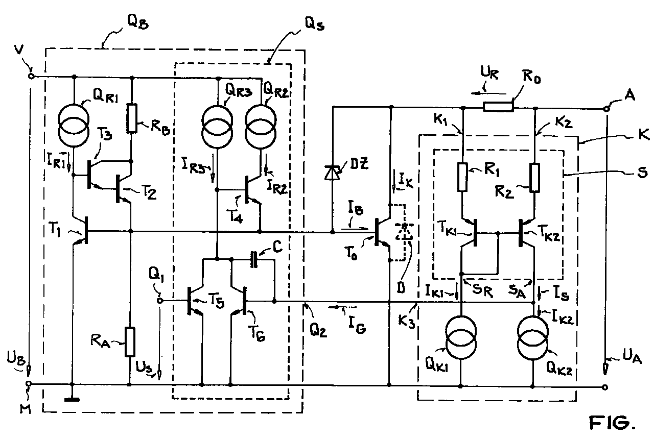
Description
Die Erfindung betrifft eine Schaltungsanordnung gemäß dem Oberbegriff des Patentanspruchs 1.The invention relates to a circuit arrangement according to the preamble of patent claim 1.
Eine derartige Schaltungsanordnung ist aus der Literaturstelle Tietze/Schenk: ![]()
![]()
Aus der Literaturstelle Millman/Grabel: ![]()
![]()
Der Erfindung liegt daher die Aufgabe zugrunde, eine Schaltungsanordnung gemäß dem Oberbegriff des Patentanspruchs 1 anzugeben, die mit einfachen Mitteln herstellbar ist und die hinsichtlich parasitärer Effekte verbesserte Eigenschaften aufweist.The invention is therefore based on the object of specifying a circuit arrangement according to the preamble of patent claim 1 is simple to produce and has improved properties with regard to parasitic effects.
Die Aufgabe wird durch die kennzeichnenden Merkmale des Patentanspruchs 1 gelöst. Vorteilhafte Ausgestaltungen und Weiterbildungen ergeben sich aus den Unteransprüchen.The object is achieved by the characterizing features of patent claim 1. Advantageous refinements and developments result from the subclaims.
Erfindungsgemäß ist der Kollektor des Open-Collector-Transistors über einen, vorzugsweise niederohmig ausgeführten, Kollektorwiderstand mit dem Open-Collector-Ausgang der Schaltungsanordnung, an dem die Ausgangsspannung ansteht, und über eine parasitare Diode mit dem Masseanschluß der Schaltungsanordnung, an dem ein Bezugspotential anliegt, verbunden. Die parasitäre Diode ist dabei aus dem Kollektorbereich des Open-Collector-Tranistors und aus einer diesen Kollektorbereich umgebenden p-dotierten Separationszone, welche zur Isolation des Open-Collector-Transistors von weiteren Schaltungsteilen der Schaltungsanordnung vorgesehen ist, gebildet. Sie ist bei positiven Spannungswerten der Ausgangsspannung in Sperrichtung geschaltet, d. h. sie ist kathodenseitig mit dem Kollektor des Open-Collector-Transistors und anodenseitig mit dem Masseanschluß der Schaltungsanordnung verbunden. Der Open-Collector-Transistor ist durch einen Basisstrom, welcher von einer mit der Basis des Open-Collector-Transistors verbundenen Basisstromquelle erzeugt wird, ansteuerbar. Er wird bei positiven Spannungswerten der Ausgangsspannung in Vorwärtsrichtung und bei negativen Spannungswerten der Ausgangsspannung in Rückwärtsrichtung betrieben, wobei er bei einen negativen Schwellspannungswert unterschreitenden Spannungswerten der Ausgangsspannung durch den Basisstrom in einen invers leitenden Zustand geschaltet wird, in welchem am Kollektorwiderstand eine Spannung abfällt, die aufgrund eines dann durch den Kollektorwiderstand fließenden Kollektorstromes des Open-Collector-Transistors so groß ist, daß die parasitäre Diode in Sperrichtung geschaltet verbleibt.According to the invention, the collector of the open collector transistor is connected via a, preferably low-resistance, collector resistor to the open collector output of the circuit arrangement, at which the output voltage is applied, and via a parasitic diode to the ground connection of the circuit arrangement, to which a reference potential is present , connected. The parasitic diode is formed from the collector region of the open collector transistor and from a p-doped separation zone surrounding this collector region, which is provided for isolating the open collector transistor from further circuit parts of the circuit arrangement. It is switched in the reverse direction at positive voltage values of the output voltage, i. H. it is connected on the cathode side to the collector of the open collector transistor and on the anode side to the ground connection of the circuit arrangement. The open collector transistor can be controlled by a base current, which is generated by a base current source connected to the base of the open collector transistor. It is operated with positive voltage values of the output voltage in the forward direction and with negative voltage values of the output voltage in the reverse direction, whereby if the voltage values of the output voltage fall below a negative threshold voltage value, it is switched into an inverse conductive state by the base current, in which a voltage drops across the collector resistor due to of a collector current of the open collector transistor then flowing through the collector resistance is so great that the parasitic diode remains switched in the reverse direction.
Die Basisstromquelle weist vorzugsweise eine mit der Basis des Open-Collector-Transistors verbundene Steuerstromquelle auf, welche über ein an einem Schalteingang der Steuerstromquelle anliegendes Schaltsignal schaltbar ist. Der Open-Collector-Transistor ist bei positiven Spannungswerten am Open-Collector-Ausgang durch Schalten der Steuerstromquelle ein- und ausschaltbar, d. h. zwischen einem niederohmigen Zustand und einem höherohmigen Zustand umschaltbar.The base current source preferably has a control current source connected to the base of the open collector transistor, which can be switched via a switching signal applied to a switching input of the control current source. The open collector transistor is switched on and off at positive voltage values at the open collector output by switching the control current source can be switched off, ie switchable between a low-resistance state and a higher-resistance state.
In einer vorteilhaften Ausgestaltung der Schaltungsanordnung weist die Basisstromquelle einen ersten Steuertransistor und eine mit dessen Kollektor verbundene erste Ruhestromquelle auf. Der erste Steuertransistor und der Open-Collector-Transistor sind dabei als Stromspiegelanordnung mit der ersten Ruhestromquelle als Referenzstromquelle verschaltet. Die Basisstromquelle weist zur niederohmigen Einkopplung des Basisstromes einen zweiten Steuertransistor auf, dessen Basis mit dem Kollektor des ersten Steuertransistors verbunden ist, dessen Emitter mit der Basis des ersten Steuertransistors verbunden ist und dessen Kollektor mit einem Versorgungsanschluß der Schaltungsanordnung, an dem eine Versorgungsspannung anliegt, verbunden ist. Sie weist zur Ansteuerung des zweiten Steuertransistors vorzugsweise einen dritten Steuertransistor auf, der mit dem zweiten Steuertransistor als Darlington-Stufe verschaltet ist.In an advantageous embodiment of the circuit arrangement, the base current source has a first control transistor and a first quiescent current source connected to its collector. The first control transistor and the open collector transistor are connected as a current mirror arrangement to the first quiescent current source as a reference current source. The base current source has a second control transistor for the low-resistance coupling of the base current, the base of which is connected to the collector of the first control transistor, the emitter of which is connected to the base of the first control transistor and the collector of which is connected to a supply connection of the circuit arrangement to which a supply voltage is applied is. To control the second control transistor, it preferably has a third control transistor which is connected to the second control transistor as a Darlington stage.
Als besonders vorteilhaft erweist es sich mittels einer Komparatorstufe ein Begrenzungssignal zur erzeugen, durch welches der Basisstrom bei einen Schwellstromwert überschreitenden Stromwerten des Kollektorstromes reduzierbar ist. Der Kollektorstrom ist auf diese Weise auf unterhalb des Schwellwertes liegende Stromwerte begrenzbar. Vorzugsweise weist die Komparatorstufe zwei mit jeweils einem Anschluß des Kollektorwiderstandes verbundene Komparatoreingänge und einen Komparatorausgang auf, an welchem das Begrenzungssignal ansteht. Dieses Begrenzungssignal wird einem mit dem Komparatorausgang der Komparatorstufe verbundenen Steuereingang der Basisstromquelle, über den der Basisstrom steuerbar ist, zugeführt.It has proven to be particularly advantageous to generate a limit signal by means of a comparator stage, by means of which the base current can be reduced if the current values of the collector current exceed a threshold current value. In this way, the collector current can be limited to current values below the threshold value. The comparator stage preferably has two comparator inputs, each connected to one connection of the collector resistor, and a comparator output, at which the limit signal is present. This limit signal is fed to a control input of the base current source, which is connected to the comparator output of the comparator stage and via which the base current can be controlled.
Die vorgestellte Schaltungsanordnung vereinigt mehrere Vorteile in sich:
- sie weist eine geringe Anzahl von Schaltungselementen auf und ist daher kostengünstig in einen integrierten Schaltkreis integrierbar,
- sie weist eine hohe Spannungsfestigkeit für negative Spannungswerte der Ausgangsspannung auf: die Spannungswerte der Ausgangsspannung am Open-Collector-Ausgang dürfen das am Masseanschluß anliegende Bezugspotential um mehr als eine Diodenflußspannung unterschreiten, wobei der zulässige Wertebereich der Ausgangsspannung durch den Kollektorwiderstand und den Kollektorstrom vorgebbar ist,
- sie weist aufgrund der Begrenzung des Kollektorstromes eine hohe Kurzschlußfestigkeit auf,
- die Spannungswerte der Ausgangsspannung sind bei eingeschaltetem und in Vorwärtsrichtung betriebenem Open-Collector-Transistor gering.
- it has a small number of circuit elements and can therefore be integrated cost-effectively into an integrated circuit,
- it has a high dielectric strength for negative voltage values of the output voltage: the voltage values of the output voltage at the open collector output may exceed the reference potential at the ground connection by more than one diode forward voltage fall below, whereby the permissible value range of the output voltage can be specified by the collector resistance and the collector current,
- due to the limitation of the collector current, it has a high short-circuit strength,
- the voltage values of the output voltage are low when the open collector transistor is switched on and operated in the forward direction.
Die erfindungsgemäße Schaltungsanordnung wird im folgenden anhand eines in der Figur gezeigten Ausführungsbeispiels näher beschrieben.The circuit arrangement according to the invention is described in more detail below with reference to an embodiment shown in the figure.
Gemäß der Figur ist der Kollektor des Open-Collector-Transistors T0 über den Kollektorwiderstand R0, an dem die Spannung UR abfällt, mit dem Open-Collector-Ausgang A der Schaltungsanordnung, an dem die Ausgangsspannung UA ansteht, verbunden, der Emitter des Open-Collector-Transistors T0 mit dem Masseanschluß M der Schaltungsanordnung, an dem ein Bezugspotential anliegt, verbunden und die Basis des Open-Collector-Transistors T0 mit der Basisstromquelle QB, die den Basisstrom IB zur Steuerung des Open-Collector-Transistors T0 liefert, verbunden. Die Zenerdiode DZ, die kathodenseitig mit dem Kollektor und anodenseitig mit der Basis des Open-Collector-Transistors T0 verbunden ist, dient zum Schutz des Open-Collector-Transistors T0 vor zu hohen Kollektor-Emitter-Spannungen. Die gesamte Schaltungsanordnung ist auf ein Halbleitersubstrat eines integrierten Schaltkreises integriert, wobei auch weitere, in der Figur nicht gezeigte, Schaltungsteile auf das gleiche Halbleitersubstrat integriert sein können. Der Kollektor des Open-Collector-Transistors T0 ist dabei von einer p-dotierten und mit dem Masseanschluß M verbundenen Separationszone umgeben und durch diese von weiteren n-dotierten Halbleiterbereichen isoliert. Die Separationszone und der Kollektorbereich des Open-Collector-Transistors T0 bilden dabei die durch gestrichelte Linien angedeutete parasitäre Diode D.According to the figure, the collector of the open collector transistor T 0 is connected via the collector resistor R 0 , at which the voltage U R drops, to the open collector output A of the circuit arrangement, at which the output voltage U A is present, which The emitter of the open collector transistor T 0 is connected to the ground terminal M of the circuit arrangement, to which a reference potential is present, and the base of the open collector transistor T 0 is connected to the base current source Q B , which supplies the base current I B for controlling the open Collector transistor T 0 supplies, connected. The Zener diode DZ, which is connected on the cathode side to the collector and on the anode side to the base of the open collector transistor T 0 , serves to protect the open collector transistor T 0 against excessive collector-emitter voltages. The entire circuit arrangement is integrated on a semiconductor substrate of an integrated circuit, it also being possible for further circuit parts, not shown in the figure, to be integrated on the same semiconductor substrate. The collector of the open collector transistor T 0 is surrounded by a p-doped and connected to the ground terminal M separation zone and isolated by this from further n-doped semiconductor regions. The separation zone and the collector region of the open collector transistor T 0 form the parasitic diode D indicated by dashed lines.
Die Basisstromquelle QB umfaßt die Steuerstromquelle QS, die erste Ruhestromquelle QR1, den ersten Steuertransistor T1, den zweite Steuertransistor T2, den dritten Steuertransistor T3, den Begrenzungswiderstand RB und den Ableitwiderstand RA. Der Emitter des ersten Steuertransistors T1 ist mit dem Masseanschluß M verbunden, der Kollektor des ersten Steuertransistors T1 ist mit der Basis des dritten Steuertransistors T3 und über die erste Ruhestromquelle QR1 mit dem Versorgungsanschluß V, dem die Versorgungsspannung UB zugeführt wird, verbunden, die Kollektoren des zweiten und des dritten Steuertransistors T2 und T3 sind über den Begrenzungswiderstand RB mit dem Versorgungsanschluß V verbunden und die Basis des ersten Steuertransistors T1 ist mit dem Emitter des zweiten Steuertransistors T2, mit der Basis des Open-Collector-Transistors T0 und über den Ableitwiderstand RA mit dem Masseanschluß M verbunden. Der Ableitwiderstand RA dient dabei zur Einstellung eines definierten Potentials an der Basis des ersten Steuertransistors T1 und der Begrenzungswiderstand RB dient zur Begrenzung des durch den zweiten Steuertransistor T2 fließenden Stromes.The base current source Q B comprises the control current source Q S , the first quiescent current source Q R1 , the first control transistor T 1 , the second control transistor T 2 , the third control transistor T 3 , the limiting resistor R B and the bleeder resistor R A. The emitter of the first control transistor T 1 is connected to the Ground terminal M connected, the collector of the first control transistor T 1 is connected to the base of the third control transistor T 3 and via the first quiescent current source Q R1 to the supply terminal V, to which the supply voltage U B is supplied, the collectors of the second and the third control transistor T 2 and T 3 are connected to the supply terminal V via the limiting resistor R B and the base of the first control transistor T 1 is connected to the emitter of the second control transistor T 2 , to the base of the open collector transistor T 0 and via the bleeder resistor R A connected to the ground terminal M. The bleeder resistor R A serves to set a defined potential at the base of the first control transistor T 1 and the limiting resistor R B serves to limit the current flowing through the second control transistor T 2 .
Die Steuerstromquelle QS umfaßt die zweite Ruhestromquelle QR2, die dritte Ruhestromquelle QR3, den vierten Steuertransistor T4, den fünften Steuertransistor T5, den sechsten Steuertransistor T6 und den Kondensator C. Dabei ist der Emitter des vierten Steuertransistors T4 mit der Basis des Open-Collector-Transistors T0 verbunden, der Kollektor des vierten Steuertransistors T4 über die zweite Ruhestromquelle QR2 mit dem Versorgungsanschluß V verbunden, die Basis des vierten Steuertransistors T4 mit den Kollektoren des fünften und sechsten Steuertransistors T5 und T6, über den Kondensator C mit dem Steuereingang Q2 der Basisstromquelle QB sowie über die dritte Ruhestromquelle QR3 mit dem Versorgungsanschluß V verbunden. Die Basis des fünften Steuertransistors TS ist mit dem Schaltanschluß Q1 der Steuerstromquelle QS, an dem eine Spannung als Schaltsignal US zum Schalten der Steuerstromquelle QS ansteht, verbunden und die Basis des sechsten Steuertransistors T6 ist mit dem Steuereingang Q2 der Basisstromquelle QB, der gleichzeitig einen Steuereingang der Steuerstromquelle QS bildet und an dem ein Strom als Begrenzungssignal IG ansteht, verbunden.The control current source Q S includes the second quiescent current source Q R2 , the third quiescent current source Q R3 , the fourth control transistor T 4 , the fifth control transistor T 5 , the sixth control transistor T 6 and the capacitor C. Here, the emitter of the fourth control transistor T 4 with the Base of the open collector transistor T 0 connected, the collector of the fourth control transistor T 4 connected to the supply terminal V via the second quiescent current source Q R2 , the base of the fourth control transistor T 4 to the collectors of the fifth and sixth control transistors T 5 and T 6 , connected to the control input Q 2 of the base current source Q B via the capacitor C and to the supply terminal V via the third quiescent current source Q R3 . The base of the fifth control transistor T S is connected to the switching terminal Q 1 of the control current source Q S , at which a voltage is present as a switching signal U S for switching the control current source Q S , and the base of the sixth control transistor T 6 is connected to the control input Q 2 Base current source Q B , which simultaneously forms a control input of the control current source Q S and at which a current is present as a limiting signal I G.
Die Komparatorstufe K umfaßt die beiden Komparatorwiderstände R1, R2, die beiden Komparatortransistoren TK1, TK2 und die beiden Konstantstromquellen QK1, QK2. Der Emitter des einen Komparatortransistors TK1 ist über den einen Komparatorwiderstand R1 mit dem einen Komparatoreingang K1 der Komparatorstufe K und mit einem, an den Kollektor des Open-Collector-Transistors T0 angeschlossenen, Anschluß des Kollektorwiderstandes R0 verbunden, der Emitter des anderen Komparatortransistors TK2 ist über den anderen Komparatorwiderstand R2 mit einem weiteren, an den Open-Collector-Ausgang A angeschlossenen, Anschluß des Kollektorwiderstandes R0 verbunden, die Basen der Komparatortransistoren TK1, TK2 sind mit dem Kollektor des einen Komparatortransistors TK1 und über die eine Konstantstromquelle QK1 mit dem Masseanschluß M verbunden und der Kollektor des anderen Komparatortransistors TK2 ist mit dem Komparatorausgang K3, der an den Steuereingang Q2 der Basisstromquelle QB angeschlossen ist, und über die andere Konstantstromquelle QK2 mit dem Masseanschluß M verbunden. Die beiden Komparatorwiderstände R1, R2 und die beiden Komparatortransistoren TK1, TK2 bilden daher eine Stromspiegelanordnung S mit dem Kollektor des einen Komparatortransistors TK1 als Referenzstromeingang SR, am dem der Strom IK1 der einen Konstantstromquelle QK1 als Referenzstrom ansteht, und mit dem Kollektor des anderen Komparatortransistors TK2 als Spiegelstromausgang SA, an dem der Spiegelstrom IS ansteht.The comparator stage K comprises the two comparator resistors R 1 , R 2 , the two comparator transistors T K1 , T K2 and the two constant current sources Q K1 , Q K2 . The emitter of a comparator transistor T K1 via the one Komparatorwiderstand R 1 with a comparator input of the comparator K 1 K and a, to the collector of the open collector transistor T0 connected, connection of the collector resistor R 0 connected, the emitter of the other comparator transistor T K2 is connected via the other comparator resistor R 2 to a further connection of the collector resistor R 0 connected to the open collector output A, the bases of the comparator transistors T K1 , T K2 are connected to the collector one of the comparator transistor T K1 and one constant current source Q K1 to the ground terminal M and the collector of the other comparator transistor T K2 is connected to the comparator output K 3 , which is connected to the control input Q 2 of the base current source Q B , and via the other constant current source Q K2 connected to the ground terminal M. The two comparator resistors R 1 , R 2 and the two comparator transistors T K1 , T K2 therefore form a current mirror arrangement S with the collector of one comparator transistor T K1 as a reference current input S R , at which the current I K1 of the one constant current source Q K1 is present as a reference current, and with the collector of the other comparator transistor T K2 as a mirror current output S A , at which the mirror current I S is present.
Die Steuertransistoren T1, T2, T3, T4, T5, T6 und der Open-Collector-Transistor T0 sind als npn-Transistoren und die Komparatortransistoren TK1, TK2 als pnp-Transistoren ausgeführt. Der Open-Collector-Transistor T0 wird daher bei positiven Spannungswerten der Ausgangsspannung UA, d. h. bei bezüglich dem Bezugspotential am Masseanschluß M positiven Potentialen am Open-Collector-Ausgang A, in vorwärtsrichtung betrieben. Er ist dann bei einem dem Bezugspotential entsprechenden Low-Pegel des Schaltsignals US eingeschaltet und bei einem, beispielsweise der Versorgungsspannung UB entsprechenden, High-Pegel des Schaltsignals US ausgeschaltet.The control transistors T 1 , T 2 , T 3 , T 4 , T 5 , T 6 and the open collector transistor T 0 are designed as npn transistors and the comparator transistors T K1 , T K2 as pnp transistors. The open collector transistor T 0 is therefore operated in the forward direction at positive voltage values of the output voltage U A , ie at potentials at the open terminal output A that are positive with respect to the reference potential at the ground connection M. It is then switched on at a low level of the switching signal U S corresponding to the reference potential and switched off at a high level of the switching signal U S , for example corresponding to the supply voltage U B.
Beim High-Pegel des Schaltsignals US ist der fünfte Steuertransistor T5 leitend und führt somit den gesamten von der dritten Ruhestromquelle QR3 lieferbaren Strom IR3 zum Masseanschluß M ab. Der vierte Steuertransistor T4 und die Steuerstromquelle QS sind folglich gesperrt und liefern daher keinen Beitrag zum Basisstrom IB. Der Basisstrom IB ist jedoch nicht gleich Null, da die Steuertransistoren T1, T2 und T3 und der Open-Collector-Transistor T0 als Stromspiegelanordnung wirken, mit der der Strom IR1 der ersten Ruhestromquelle QR1 als Kollektorstrom IK des Open-Collector-Transistors T0 zum Open-Collector-Ausgang A gespiegelt wird. Das Spiegelverhältnis - das Verhältnis aus dem Kollektorstrom IK des Open-Collector-Transistors T0 und dem Strom IR1 der ersten Ruhestromquelle QR1 -ist durch das Verhältnis aus der Emitterfläche des Open-Collector-Transistors T0 und der Emitterfläche des ersten Steuertransistors T1 auf einen Wert von beispielsweise 20 festgelegt. Bei einem Strom IR1 der ersten Ruhestromquelle QR1 von beispielsweise 75 µA beträgt der Kollektorstrom IK dann 1,5 mA. Dieses ist der minimale durch den Open-Collector-Transistor T0 fließende Kollektorstrom IK, d. h. der Open-Collector-Transistor T0 ist im ausgeschalteten Zustand nicht vollständig sperrend, sondern er befindet sich lediglich in einem höherohmigen Zustand als im eingeschalteten Zustand.At the high level of the switching signal U S of the fifth control transistor T 5 is conductive, and thus executes all of the third quiescent current source Q R3 deliverable current I R3 to the ground terminal from M. The fourth control transistor T 4 and the control current source Q S are consequently blocked and therefore make no contribution to the base current I B. However, the base current I B is not equal to zero, since the control transistors T 1 , T 2 and T 3 and the open collector transistor T 0 act as a current mirror arrangement with which the current I R1 of the first quiescent current source Q R1 as the collector current I K des Open collector transistor T 0 is mirrored to open collector output A. The mirror ratio - the ratio of the collector current I K of the open collector transistor T 0 and the current I R1 of the first quiescent current source Q R1 - is set to a value of, for example, 20 by the ratio of the emitter area of the open collector transistor T 0 and the emitter area of the first control transistor T 1 . With a current I R1 of the first quiescent current source Q R1 of, for example, 75 μA, the collector current I K is then 1.5 mA. This is the minimum collector current I K flowing through the open collector transistor T 0 , ie the open collector transistor T 0 is not completely blocking in the switched-off state, but is only in a higher-resistance state than in the switched-on state.
Bei einem Low-Pegel des Schaltsignals US ist der fünfte Steuertransistor T5 gesperrt, so daß der Strom IR3 der dritten Ruhestromquelle QR3 der Basis des vierten Steuertransistors T4 zugeführt wird. Dieser ist daher leitend und leitet folglich den Strom IR2 der zweiten Ruhestromquelle QR2, der beispielsweise etwa 3 mA beträgt, zur Basis des Open-Collector-Transistors T0, welcher hierdurch eingeschaltet, d. h. in einen niederohmigen Zustand geschaltet wird. Falls dem Steuereingang Q2 gleichzeitig das Begrenzungssignal IG zugeführt wird, wird ein Teil des Stromes IR3 der dritten Ruhestromquelle QR3 über den sechsten Steuertransistor T6 zum Masseanschluß M abgeleitet, so daß nur noch ein Teil des von der zweiten Ruhestromquelle QR2 lieferbaren Stromes IR2 über den vierten Steuertransistor T4 der Basis des Open-Collector-Transistors T0 zugeführt werden kann, d. h. der Basisstrom IB und folglich auch der Kollektorstrom IK werden durch das Begrenzungssignal IG reduziert.When the switching signal U S is low, the fifth control transistor T 5 is blocked, so that the current I R3 of the third quiescent current source Q R3 is supplied to the base of the fourth control transistor T 4 . This is therefore conductive and consequently conducts the current I R2 of the second quiescent current source Q R2 , which is, for example, about 3 mA, to the base of the open collector transistor T 0 , which is thereby switched on, ie switched to a low-resistance state. If the limit signal I G is supplied to the control input Q 2 at the same time, part of the current I R3 of the third quiescent current source Q R3 is derived via the sixth control transistor T 6 to the ground terminal M, so that only part of the current available from the second quiescent current source Q R2 Current I R2 can be supplied via the fourth control transistor T 4 to the base of the open collector transistor T 0 , ie the base current I B and consequently also the collector current I K are reduced by the limiting signal I G.
Die Widerstandswerte des Kollektorwiderstandes R0 und der Komparatorwiderstände R1, R2 sind derart gewählt, daß der Strom IK1 der einen Konstantstromquelle QK1 und der Spiegelstrom IS der Stromspiegelanordnung S dann gleich sind, wenn der Kollektorstrom IK des Open-Collector-Transistors T0 gleich einem Schwellstromwert von beispielsweise 80 mA ist. Bei einem Widerstandswert des Kollektorwiderstandes R0 von beispielsweise 3 Ω beträgt der eine Komparatorwiderstand R1 beispielsweise 2 kΩ und der andere Komparatorwiderstand R2 11,6 kΩ. Die beiden Konstantstromquellen QK1, QK2 liefern lediglich geringe Ströme IK1, IK2, die gleich sind und beispielsweise jeweils 25 µA betragen, so daß die Schaltungsanordnung durch die Komparatorstufe K nur geringfügig belastet wird. Bei einem den Schwellstromwert überschreitenden Stromwert des Kollektorstromes IK ist der Spannungsabfall zwischen dem Open-Collector-Ausgang A und dem Emitter des einen Komparatortransistors TK1 größer als der Spannungsabfall zwischen dem Open-Collector-Ausgang A und dem Emitter des anderen Komparatortransistors TK2. Folglich ist auch der Spiegelstrom IS größer als der Strom IK1 der einen Konstantstromquelle QK1. Der den Strom IK2 der zweiten Konstantstromquelle QK2 überschreitende Anteil des Spiegelstromes IS wird dann als Begrenzungssignal IG dem Steuereingang Q2 der Basisstromquelle QB zugeführt. Der Kollektorstrom IK wird daraufhin durch Reduzierung des Basisstromes IB auf einen unterhalb des Schwellstromwerts liegenden Stromwert begrenzt. Der Kondensator C verhindert dabei, daß die Schaltungsanordnung hierdurch zum Schwingen angeregt wird.The resistance values of the collector resistor R 0 and the comparator resistors R 1 , R 2 are selected such that the current I K1 of the one constant current source Q K1 and the mirror current I S of the current mirror arrangement S are the same when the collector current I K of the open collector Transistor T 0 is equal to a threshold current value of 80 mA, for example. With a resistance value of the collector resistance R 0 of, for example, 3 Ω, the one comparator resistance R 1 is for example 2 kΩ and the other comparator resistance R 2 is 11.6 kΩ. The two constant current sources Q K1 , Q K2 only supply small currents I K1 , I K2 , which are the same and, for example, each amount to 25 μA, so that the circuit arrangement is only slightly loaded by the comparator stage K. If the current value of the collector current I K exceeds the threshold current value, the voltage drop between the open collector output A and the emitter of the one comparator transistor T K1 is greater than the voltage drop between the open collector output A and the emitter of the other comparator transistor T K2 . Consequently, the mirror current I S is also greater than the current I K1 of the one constant current source Q K1 . The portion of the mirror current I S which exceeds the current I K2 of the second constant current source Q K2 is then fed to the control input Q 2 of the base current source Q B as the limiting signal I G. The collector current I K is then limited by reducing the base current I B to a current value below the threshold current value. The capacitor C prevents the circuit arrangement from being excited to oscillate as a result.
Der Open-Collector-Transistor T0 wird bei negativen Spannungswerten der Ausgangsspannung UA in Rückwärtsrichtung, d. h. invers betrieben. Er wird bei Spannungswerten der Ausgangsspannung UA, die eine negative Schwellwertspannung, welche um eine Diodenflußspannung (0,7 V) kleiner als das Bezugspotential ist, unterschreiten, in einen invers leitenden Zustand geschaltet. Der Kollektorstrom IK fließt dann vom Kollektor des Open-Collector-Transistors T0 durch den Kollektorwiderstand R0 zum Open-Collector-Ausgang A, so daß er Open-Collector-Transistor T0 und die Steuertransistoren T1, T2, T3 nicht mehr als Stromspiegelanordnung wirken. Da die parasitäre Diode D sperrend sein soll, muß die am Kollektorwiderstand R0 abfallende Spannung UR so groß sein, daß sich am Kollektor der Open-Collector-Transistors T0 ein Potential einstellt, welches das Bezugspotential am Masseanschluß M und folglich auch das Potential an der Separationszone um weniger als eine Diodenflußspannung unterschreitet. Der Kollektorstrom IK muß, da die Spannung UR von ihm abhängig ist, entsprechend groß ausgelegt sein. Die parasitäre Diode D ist dann für alle Spannungswerte der Ausgangsspannung UA, die innerhalb eines zulässigen Wertebereichs von beispielsweise -1 V bis 29 V liegen, in Sperrichtung geschaltet. Der kleinste Wert des zulässigen Wertebereichs ist dabei durch den Kollektorstrom IK und den Kollektorwiderstand R0 vorgegeben. Der Kollektorwiderstand R0 darf jedoch, da die Ausgangsspannung UA bei in Vorwärtsrichtung leitendem Open-Collector-Transistor T0 einen Maximalwert von beispielsweise 0,5 V nicht überschreiten soll, nicht zu groß dimensioniert sein. Daher muß der Kollektorstrom IK durch die Wahl eines ausreichend großen Basisstromes IB entsprechend groß ausgelegt sein. Die Stromverstärkung des Open-Collector-Transistors T0 ist beim Betrieb in Rückwärtsrichtung wesentlich kleiner als beim Betrieb in Vorwärtsrichtung. Demzufolge wird beispielsweise zur Erzeugung eines Kollektorstromes IK von -200 mA ein Basisstrom IB von ca. 20 mA benötigt. Bei einer Ausgangsspannung UA von -1 V und einem Kollektorwiderstand R0 von 3 Ω erhält man dann am Kollektor des Open-Collector-Transistors T0 ein Potential von -0,4 V, d. h. die parasitäre Diode D bleibt gesperrt. Die Basis-Kollektor-Diode des Open-Collector-Transistors T0 ist hingegen leitend, so daß der erste Steuertransistor T1, an dessen Basis folglich ein Potential von ca. 0,3 V anliegt, gesperrt ist. Daher wird der gesamte Strom IR1 der ersten Ruhestromquelle QR1 zu der aus dem zweiten und dritten Steuertransistor T2, T3 gebildeten Darlington-Stufe geführt und durch diese um ein Vielfaches verstärkt. Dieser um ein Vielfaches auf ca. 20 mA verstärkte Strom, der von der Versorgungsspannung UB geliefert wird, wird durch den Widerstand RB begrenzt und dann der Basis des Open-Collector-Transistors T0 als Basisstrom IB zugeführt.The open collector transistor T 0 is operated in the reverse direction, ie inversely, at negative voltage values of the output voltage U A. It is switched into an inversely conductive state at voltage values of the output voltage U A which fall below a negative threshold voltage which is less than the reference potential by a diode forward voltage (0.7 V). The collector current I K then flows from the collector of the open collector transistor T 0 through the collector resistor R 0 to the open collector output A, so that it is the open collector transistor T 0 and the control transistors T 1 , T 2 , T 3 no longer act as a current mirror arrangement. Since the parasitic diode D is supposed to be blocking, the voltage U R dropping across the collector resistor R 0 must be so great that the open collector transistor T 0 has a potential at the collector which represents the reference potential at the ground connection M and consequently also the potential at the separation zone is less than a diode forward voltage. The collector current I K , since the voltage U R depends on it, must be designed to be correspondingly large. The parasitic diode D is then switched in the reverse direction for all voltage values of the output voltage U A which lie within a permissible value range of, for example, -1 V to 29 V. The smallest value of the permissible value range is predetermined by the collector current I K and the collector resistance R 0 . However, since the output voltage U A should not exceed a maximum value of, for example, 0.5 V when the open collector transistor T 0 is conductive in the forward direction, the collector resistance R 0 must not be too large. Therefore, the collector current I K must be designed to be correspondingly large by choosing a sufficiently large base current I B. The current gain of the open collector transistor T 0 is significantly smaller when operating in the reverse direction than when operating in the forward direction. Accordingly, for example, to generate a collector current I K of -200 mA, a base current I B of approx. 20 mA is required. With an output voltage U A of -1 V and a collector resistance R 0 of 3 Ω, a potential of -0.4 V is then obtained at the collector of the open collector transistor T 0 , ie the parasitic diode D remains blocked. The base-collector diode of the open-collector transistor T 0 , on the other hand, is conductive, so that the first control transistor T 1 , at the base of which a potential of approximately 0.3 V is consequently present, is blocked. Therefore, the entire current I R1 of the first quiescent current source Q R1 is led to the Darlington stage formed from the second and third control transistor T 2 , T 3 and amplified by it many times over. This current, amplified by a multiple to approximately 20 mA, which is supplied by the supply voltage U B , is limited by the resistor R B and then supplied to the base of the open collector transistor T 0 as the base current I B.
Claims (11)
Applications Claiming Priority (2)
| Application Number | Priority Date | Filing Date | Title |
|---|---|---|---|
| DE19620564 | 1996-05-22 | ||
| DE19620564A DE19620564C1 (en) | 1996-05-22 | 1996-05-22 | Integrated circuit using npn open-collector transistor |
Publications (3)
| Publication Number | Publication Date |
|---|---|
| EP0809360A2 true EP0809360A2 (en) | 1997-11-26 |
| EP0809360A3 EP0809360A3 (en) | 1998-07-15 |
| EP0809360B1 EP0809360B1 (en) | 2000-08-02 |
Family
ID=7794983
Family Applications (1)
| Application Number | Title | Priority Date | Filing Date |
|---|---|---|---|
| EP97107428A Expired - Lifetime EP0809360B1 (en) | 1996-05-22 | 1997-05-06 | Integrated circuit with an NPN-type open collector transistor |
Country Status (5)
| Country | Link |
|---|---|
| US (1) | US5973513A (en) |
| EP (1) | EP0809360B1 (en) |
| JP (1) | JPH10107604A (en) |
| DE (2) | DE19620564C1 (en) |
| ES (1) | ES2149529T3 (en) |
Families Citing this family (1)
| Publication number | Priority date | Publication date | Assignee | Title |
|---|---|---|---|---|
| FR3039905B1 (en) | 2015-08-07 | 2019-01-25 | STMicroelectronics (Alps) SAS | VOLTAGE SOURCE |
Family Cites Families (6)
| Publication number | Priority date | Publication date | Assignee | Title |
|---|---|---|---|---|
| JPS57121321A (en) * | 1981-01-21 | 1982-07-28 | Yamatake Honeywell Co Ltd | Open collector output type digital circuit |
| DE3237141C1 (en) * | 1982-10-07 | 1983-07-28 | Danfoss A/S, 6430 Nordborg | Control device for a switching transistor |
| EP0190925B1 (en) * | 1985-02-08 | 1993-12-29 | Kabushiki Kaisha Toshiba | A protection circuit for an insulated gate bipolar transistor |
| GB2204445B (en) * | 1987-03-06 | 1991-04-24 | Texas Instruments Ltd | Semiconductor switch |
| US4965466A (en) * | 1989-07-19 | 1990-10-23 | Motorola, Inc. | Substrate injection clamp |
| JPH03270407A (en) * | 1990-03-20 | 1991-12-02 | Fujitsu Ltd | Semiconductor integrated circuit |
-
1996
- 1996-05-22 DE DE19620564A patent/DE19620564C1/en not_active Expired - Fee Related
-
1997
- 1997-05-06 ES ES97107428T patent/ES2149529T3/en not_active Expired - Lifetime
- 1997-05-06 EP EP97107428A patent/EP0809360B1/en not_active Expired - Lifetime
- 1997-05-06 DE DE59702101T patent/DE59702101D1/en not_active Expired - Lifetime
- 1997-05-07 US US08/852,473 patent/US5973513A/en not_active Expired - Lifetime
- 1997-05-16 JP JP9161767A patent/JPH10107604A/en active Pending
Also Published As
| Publication number | Publication date |
|---|---|
| US5973513A (en) | 1999-10-26 |
| DE19620564C1 (en) | 1997-07-10 |
| EP0809360B1 (en) | 2000-08-02 |
| JPH10107604A (en) | 1998-04-24 |
| DE59702101D1 (en) | 2000-09-07 |
| ES2149529T3 (en) | 2000-11-01 |
| EP0809360A3 (en) | 1998-07-15 |
Similar Documents
| Publication | Publication Date | Title |
|---|---|---|
| DE1812292C3 (en) | Circuit arrangement for gain control | |
| EP0093996B1 (en) | Level conversion circuitry | |
| DE2727537A1 (en) | THRESHOLD DETECTOR | |
| WO1997033365A1 (en) | Operational amplifier | |
| DE60130696T2 (en) | Biasing circuit for a field effect transistor | |
| DE3537920A1 (en) | ELECTRONIC VOLTAGE STABILIZER WITH PROTECTION AGAINST TRANSITION OVERVOLTAGES WHOSE POLARITY IS OPPOSITE TO THE POLARITY OF THE GENERATOR, ESPECIALLY FOR USE IN MOTOR VEHICLES | |
| EP0106088B1 (en) | Integrated semiconductor amplifier circuit | |
| EP0334447B1 (en) | Schmitt-trigger circuit | |
| EP1033809B1 (en) | Differential amplifier | |
| DE1537185B2 (en) | AMPLITUDE FILTER | |
| DE2924171C2 (en) | ||
| DE2853581C2 (en) | Emitter follower circuit | |
| DE2506034A1 (en) | CIRCUIT ARRANGEMENT FOR ELECTRONIC CONNECTION OF AN AC VOLTAGE | |
| DE3210661A1 (en) | AMPLIFIER | |
| DE3615383A1 (en) | A CIRCUIT TO SHIFT THE INPUT LEVEL OF A DIGITAL-ANALOG CONVERTER | |
| EP0809360B1 (en) | Integrated circuit with an NPN-type open collector transistor | |
| DE69024711T2 (en) | Amplifier circuit | |
| DE2056078C3 (en) | Feedback interlock switch | |
| WO1993006541A1 (en) | Device for generating intermediate voltages | |
| DE2820416A1 (en) | SWITCH KEIS | |
| DE2148880C2 (en) | Power source in integrated circuit technology | |
| EP0541164A1 (en) | Amplifier | |
| EP0676846B1 (en) | Switch with a bipolar transistor as first switching element | |
| EP0185377B1 (en) | Signalling circuit | |
| DE3615513A1 (en) | DIGITAL-ANALOG CONVERTER FOR LOW VOLTAGE VALUES |
Legal Events
| Date | Code | Title | Description |
|---|---|---|---|
| PUAI | Public reference made under article 153(3) epc to a published international application that has entered the european phase |
Free format text: ORIGINAL CODE: 0009012 |
|
| AK | Designated contracting states |
Kind code of ref document: A2 Designated state(s): DE ES FR GB IT SE |
|
| PUAL | Search report despatched |
Free format text: ORIGINAL CODE: 0009013 |
|
| AK | Designated contracting states |
Kind code of ref document: A3 Designated state(s): DE ES FR GB IT SE |
|
| 17P | Request for examination filed |
Effective date: 19980808 |
|
| RAP1 | Party data changed (applicant data changed or rights of an application transferred) |
Owner name: TEMIC SEMICONDUCTOR GMBH |
|
| GRAG | Despatch of communication of intention to grant |
Free format text: ORIGINAL CODE: EPIDOS AGRA |
|
| GRAG | Despatch of communication of intention to grant |
Free format text: ORIGINAL CODE: EPIDOS AGRA |
|
| GRAH | Despatch of communication of intention to grant a patent |
Free format text: ORIGINAL CODE: EPIDOS IGRA |
|
| 17Q | First examination report despatched |
Effective date: 19991109 |
|
| GRAH | Despatch of communication of intention to grant a patent |
Free format text: ORIGINAL CODE: EPIDOS IGRA |
|
| ITF | It: translation for a ep patent filed | ||
| GRAA | (expected) grant |
Free format text: ORIGINAL CODE: 0009210 |
|
| AK | Designated contracting states |
Kind code of ref document: B1 Designated state(s): DE ES FR GB IT SE |
|
| REF | Corresponds to: |
Ref document number: 59702101 Country of ref document: DE Date of ref document: 20000907 |
|
| GBT | Gb: translation of ep patent filed (gb section 77(6)(a)/1977) |
Effective date: 20000925 |
|
| ET | Fr: translation filed | ||
| REG | Reference to a national code |
Ref country code: ES Ref legal event code: FG2A Ref document number: 2149529 Country of ref document: ES Kind code of ref document: T3 |
|
| RAP2 | Party data changed (patent owner data changed or rights of a patent transferred) |
Owner name: ATMEL GERMANY GMBH |
|
| PLBE | No opposition filed within time limit |
Free format text: ORIGINAL CODE: 0009261 |
|
| STAA | Information on the status of an ep patent application or granted ep patent |
Free format text: STATUS: NO OPPOSITION FILED WITHIN TIME LIMIT |
|
| 26N | No opposition filed | ||
| REG | Reference to a national code |
Ref country code: GB Ref legal event code: IF02 |
|
| PGFP | Annual fee paid to national office [announced via postgrant information from national office to epo] |
Ref country code: ES Payment date: 20080529 Year of fee payment: 12 |
|
| PGFP | Annual fee paid to national office [announced via postgrant information from national office to epo] |
Ref country code: IT Payment date: 20080524 Year of fee payment: 12 |
|
| PGFP | Annual fee paid to national office [announced via postgrant information from national office to epo] |
Ref country code: SE Payment date: 20080513 Year of fee payment: 12 |
|
| PGFP | Annual fee paid to national office [announced via postgrant information from national office to epo] |
Ref country code: GB Payment date: 20080522 Year of fee payment: 12 |
|
| GBPC | Gb: european patent ceased through non-payment of renewal fee |
Effective date: 20090506 |
|
| REG | Reference to a national code |
Ref country code: FR Ref legal event code: ST Effective date: 20100129 |
|
| PG25 | Lapsed in a contracting state [announced via postgrant information from national office to epo] |
Ref country code: FR Free format text: LAPSE BECAUSE OF NON-PAYMENT OF DUE FEES Effective date: 20090602 |
|
| PGFP | Annual fee paid to national office [announced via postgrant information from national office to epo] |
Ref country code: FR Payment date: 20080526 Year of fee payment: 12 |
|
| PG25 | Lapsed in a contracting state [announced via postgrant information from national office to epo] |
Ref country code: GB Free format text: LAPSE BECAUSE OF NON-PAYMENT OF DUE FEES Effective date: 20090506 |
|
| REG | Reference to a national code |
Ref country code: ES Ref legal event code: FD2A Effective date: 20090507 |
|
| PG25 | Lapsed in a contracting state [announced via postgrant information from national office to epo] |
Ref country code: ES Free format text: LAPSE BECAUSE OF NON-PAYMENT OF DUE FEES Effective date: 20090507 |
|
| PG25 | Lapsed in a contracting state [announced via postgrant information from national office to epo] |
Ref country code: IT Free format text: LAPSE BECAUSE OF NON-PAYMENT OF DUE FEES Effective date: 20090506 |
|
| PG25 | Lapsed in a contracting state [announced via postgrant information from national office to epo] |
Ref country code: SE Free format text: LAPSE BECAUSE OF NON-PAYMENT OF DUE FEES Effective date: 20090507 |
|
| PGFP | Annual fee paid to national office [announced via postgrant information from national office to epo] |
Ref country code: DE Payment date: 20120529 Year of fee payment: 16 |
|
| PG25 | Lapsed in a contracting state [announced via postgrant information from national office to epo] |
Ref country code: DE Free format text: LAPSE BECAUSE OF NON-PAYMENT OF DUE FEES Effective date: 20131203 |
|
| REG | Reference to a national code |
Ref country code: DE Ref legal event code: R119 Ref document number: 59702101 Country of ref document: DE Effective date: 20131203 |