EP0809353B1 - Verstärker zur Unterdrückung von Störgeräusch zwischen Schaltungssystemen - Google Patents
Verstärker zur Unterdrückung von Störgeräusch zwischen Schaltungssystemen Download PDFInfo
- Publication number
- EP0809353B1 EP0809353B1 EP97107186A EP97107186A EP0809353B1 EP 0809353 B1 EP0809353 B1 EP 0809353B1 EP 97107186 A EP97107186 A EP 97107186A EP 97107186 A EP97107186 A EP 97107186A EP 0809353 B1 EP0809353 B1 EP 0809353B1
- Authority
- EP
- European Patent Office
- Prior art keywords
- circuit
- amplifier
- reference potential
- input terminal
- resistor
- Prior art date
- Legal status (The legal status is an assumption and is not a legal conclusion. Google has not performed a legal analysis and makes no representation as to the accuracy of the status listed.)
- Expired - Lifetime
Links
- 230000008878 coupling Effects 0.000 claims description 19
- 238000010168 coupling process Methods 0.000 claims description 19
- 238000005859 coupling reaction Methods 0.000 claims description 19
- 239000003990 capacitor Substances 0.000 claims description 13
- 238000004519 manufacturing process Methods 0.000 description 10
- 230000005540 biological transmission Effects 0.000 description 1
- 230000001419 dependent effect Effects 0.000 description 1
- 238000000034 method Methods 0.000 description 1
- 230000005855 radiation Effects 0.000 description 1
Images


Classifications
-
- H—ELECTRICITY
- H03—ELECTRONIC CIRCUITRY
- H03L—AUTOMATIC CONTROL, STARTING, SYNCHRONISATION OR STABILISATION OF GENERATORS OF ELECTRONIC OSCILLATIONS OR PULSES
- H03L7/00—Automatic control of frequency or phase; Synchronisation
-
- H—ELECTRICITY
- H03—ELECTRONIC CIRCUITRY
- H03F—AMPLIFIERS
- H03F1/00—Details of amplifiers with only discharge tubes, only semiconductor devices or only unspecified devices as amplifying elements
- H03F1/26—Modifications of amplifiers to reduce influence of noise generated by amplifying elements
-
- H—ELECTRICITY
- H03—ELECTRONIC CIRCUITRY
- H03F—AMPLIFIERS
- H03F3/00—Amplifiers with only discharge tubes or only semiconductor devices as amplifying elements
- H03F3/45—Differential amplifiers
- H03F3/45071—Differential amplifiers with semiconductor devices only
- H03F3/45076—Differential amplifiers with semiconductor devices only characterised by the way of implementation of the active amplifying circuit in the differential amplifier
- H03F3/45475—Differential amplifiers with semiconductor devices only characterised by the way of implementation of the active amplifying circuit in the differential amplifier using IC blocks as the active amplifying circuit
-
- H—ELECTRICITY
- H03—ELECTRONIC CIRCUITRY
- H03F—AMPLIFIERS
- H03F3/00—Amplifiers with only discharge tubes or only semiconductor devices as amplifying elements
- H03F3/45—Differential amplifiers
- H03F3/45071—Differential amplifiers with semiconductor devices only
- H03F3/45479—Differential amplifiers with semiconductor devices only characterised by the way of common mode signal rejection
- H03F3/45928—Differential amplifiers with semiconductor devices only characterised by the way of common mode signal rejection using IC blocks as the active amplifying circuit
- H03F3/45968—Differential amplifiers with semiconductor devices only characterised by the way of common mode signal rejection using IC blocks as the active amplifying circuit by offset reduction
- H03F3/45973—Differential amplifiers with semiconductor devices only characterised by the way of common mode signal rejection using IC blocks as the active amplifying circuit by offset reduction by using a feedback circuit
-
- H—ELECTRICITY
- H03—ELECTRONIC CIRCUITRY
- H03F—AMPLIFIERS
- H03F2200/00—Indexing scheme relating to amplifiers
- H03F2200/189—Indexing scheme relating to amplifiers the ground, reference or shield potential difference between different chips being controlled
-
- H—ELECTRICITY
- H03—ELECTRONIC CIRCUITRY
- H03F—AMPLIFIERS
- H03F2200/00—Indexing scheme relating to amplifiers
- H03F2200/372—Noise reduction and elimination in amplifier
Definitions
- the present invention relates to an amplifier for canceling noise generated between circuit systems, and particularly to an analog amplifier, which is applied to, for example, an audio circuit, for preventing noise from being generated to an analog output signal to be sent to the other systems having a different reference potential based on a difference between two circuit systems in the reference potential.
- the circuit is formed on a plurality of circuit boards, and these plurality of circuit systems are connected by a connection line.
- the connection line In the case of connecting the reference potentials, e.g., ground potentials, of different circuit systems, by the connection line, there occurs a case in which a current flows between the reference potentials or a case in which the connection line acts as an antenna to cause noise to be carried on the connection line.
- a potential difference occurs between the reference potentials of the different circuit systems.
- the potential difference generally includes an unfavorable noise component. As a result, particularly, the analog circuit is largely damaged.
- FIG. 15 shows a mechanism in which noise is generated between reference potentials of two circuit systems each formed on a different circuit boards, that is, ground potentials.
- Arrows illustrated between two circuit systems 111 and 112 show a direction where a signal is received and transmitted. It is assumed that the total amount of current I1 flows in transmitting a signal from the first circuit system 111 to the second signal system 112 and that the total amount of current 12 flows in transmitting a signal from the second circuit system 112 to the first circuit system 111. As a result, the current of I1 - I2 flows into a connection line between reference potentials 113 and 114 of two circuit boards in a direction from the first circuit system 111 to the second circuit system 112.
- connection line serves as an antenna
- a current In which is generated by noise to enter in a form of a radio wave
- currents I1 and I2 are surely generated in receiving and transmitting the signal.
- the current I1 and I2 are increased as the system is enlarged and the number of digital circuits is increased.
- the current In is also increased as the number of the digital circuits is increased, unnecessary amount of radiation is increased and the reference potential connection line becomes long.
- impedance Z is also increased as the connection line between the reference potentials becomes long. Therefore, it can be considered that the reference potential difference Vx becomes large as the scale of the system and the digital section of the system become large.
- the DC component of the reference potential difference Vx can be cut by a coupling condenser.
- the AC component is superimposed on the signal component in receiving and transmitting the analog signal. As a result, transmission property is deteriorated.
- FIG. 14 shows one example of such a signal receiving and transmitting circuit.
- This type of the signal receiving and transmitting circuit comprises an amplifier, a differential amplifier 104, and two signal lines.
- the amplifier is provided at an output stage of the first circuit system 111 of the signal output side.
- the amplifier comprises inverting type analog amplifiers 101, 102, and 103 for generating differential signals eo+ and eo- of a signal eil to be transmitted.
- the differential amplifier 104 is provided at an input stage of the second circuit system 112 of the signal input side.
- the differential signals eo+ and eo- are input to the differential amplifier 104.
- Two signal lines transmit the differential signals.
- This type of the circuit transmits the signal in the form of a differential signal, and receives the signal in the form of a differential signal.
- an output potential eo2 of the differential amplifier 104 can be obtained as follows.
- noise Vx can be prevented from appearing in the output potential eo2.
- EP-0 482 291 discloses an isolator circuit for an audio system having an operational amplifier provided between a signal source and an amplifier. A capacitor and a resistor connected in series are connected between each input of the operational amplifier and the signal source. A buffer amplifier is provided between the capacitor and the resistor of each input line of the operational amplifier.
- An object of the present invention is to provide a circuit for receiving and transmitting a signal without an increasing manufacturing cost and a circuit occupying area and generating a noise component.
- the object can be achieved by the following structure.
- FIG. 1 shows an embodiment of the present invention.
- the same reference numerals are added to the structural elements in common to each other, and the specific explanation will be omitted.
- each of first and second circuit systems 11 and 12 is formed on a different circuit board.
- the reference potential of the first circuit system 11 is different from that of the second circuit system 12.
- An analog signal is transmitted from the first circuit system 11 to the second circuit system 12.
- a reference potential 13 of the first circuit system 11 and a reference potential 14 of the second circuit system 12 are normally set to a ground potential. In FIG. 1, these reference potentials are shown by a different ground potential mark. These two systems are electrically connected to each other through impedance Z formed between the reference potentials 13 and 14. Noise Vx is generated between both ends of impedance Z by the above-mentioned reason.
- a signal eil is supplied to an input terminal of an analog amplifier 1 whose gain is A.
- An output signal of the analog amplifier 1 is transmitted to the second circuit system 12 to be supplied to an input terminal of an analog amplifier 2.
- an input signal of the analog amplifier 2 of the second circuit system becomes A x eil + Vx by providing that the reference potential of the second circuit system is set as a reference.
- the difference Vx between the reference potentials 13 and 14 of two circuit systems is directly input to the second circuit system 12.
- the reference potential difference canceling circuit 3 whose gain is 1/A is provided in the first circuit system 11.
- An input terminal of the circuit 3 is connected to a ground point 14, which is the reference potential of the second circuit system 12.
- an output signal of the circuit 3 is supplied to the input terminal of the analog amplifier 1 with the signal eil.
- noise component Vx can be removed.
- one analog amplifier and the simple reference potential difference canceling circuit are used, so that the signal can be received and transmitted between the different circuit systems without generating the noise component.
- it is unnecessary to provide an amplifier for generating a differential signal and an amplifier for receiving the differential signal.
- the manufacturing cost and the circuit occupying area can be reduced.
- FIG. 2 shows an inverting type amplifier as the analog amplifier 1 shown in FIG. 1.
- the signal eil is supplied to one end of a resistor R1, and the other end of the resistor R1 is connected to an inverting input terminal of an operational amplifier 21.
- the inverting input terminal of the operational amplifier 21 is connected to one end of a resistor R2, and the other end of the resistor R2 is connected to an output terminal of the operational amplifier 21.
- the output terminal of the operational amplifier 21 is connected to an input terminal of the analog amplifier 2 of the second circuit system.
- the reference potential 14 of the second circuit system 12 is supplied to the input terminal IN of the canceling circuit 3 of the first circuit system 11.
- the canceling circuit 3 is a potential divider using the resistor.
- a resistor R3 is provided between the input terminal IN and the output terminal OUT.
- a resistor R4 is provided between the output terminal OUT and the reference potential 13 of the first circuit system.
- the output terminal OUT of the canceling circuit 3 is connected to a non-inverting input terminal of the operational amplifier 21.
- the gain which is from the input terminal IN of the canceling circuit 3 to the output terminal of the analog amplifier 1, becomes 1.
- one analog amplifier and the simple reference potential difference canceling circuit are used, so that the signal can be received and transmitted between the different circuit systems without generating the noise component.
- it is unnecessary to provide an amplifier for generating a differential signal and an amplifier for receiving the differential signal.
- the manufacturing cost and the circuit occupying area can be reduced.
- FIG. 3 shows an inverting input type amplifier as the analog amplifier 1 of a single power supply.
- the analog amplifier 1 of this embodiment comprises an operational amplifier 21, and resistors R1 and R2, and is the same as the analog amplifier of FIG. 2.
- the signal eil is supplied to one end of the resistor R1, and the other end of the resistor R1 is connected to an inverting input terminal of the operational amplifier 21.
- An output terminal of the operational amplifier 21 is connected to the input terminal of the analog amplifier 2 of the second circuit system through a coupling condenser C1.
- the reference potential 14 of the second circuit system 12 is supplied to the input terminal IN of the canceling circuit 3 of the first circuit system 11 through a coupling condenser C2.
- a resistor R15 is provided between the input terminal IN and the output terminal OUT.
- a resistor R13 is provided between a power supply potential VDD of the first circuit system and the output terminal OUT.
- a resistor R14 is provided between the output terminal OUT and the reference potential of the first circuit system. The output terminal OUT of the canceling circuit 3 is connected to the non-inverting input terminal of the operational amplifier 21.
- the input signal eil of the analog amplifier 1 swings around a ground potential, positive and negative power-supply sources are needed as a power supply for the analog amplifier 1.
- the input signal eil cannot swing around the ground potential. Due to this, another reference potential Vref must be provided.
- the reference potential Vref is normally set to a half of the power supply potential.
- es is an input signal, which does not include a DC component.
- the input signal eil swings around the reference potential Vref.
- the reference potential Vref is a DC value.
- the Reference potential Vref is provided on a common junction of the resistors R13 and R14 by dividing the potential between the power supply potential VDD and the reference potential 13. In a case where the power supply potential VDD is unstable, there can be considered a method in which a stable potential is created and the reference potential Vref is provided by dividing the potential between the stable potential and the reference potential 13.
- the input terminal IN of the canceling circuit 3 shown in FIG. 3 is connected to the reference potential 14 of the second circuit system through the coupling condenser C2. Due to this, only AC component of noise Vx is input to the canceling circuit 3. In other words, DC component of noise Vx cannot be canceled.
- the output terminal of the analog amplifier 1 and the input terminal of the analog amplifier 2 are connected to each other through the coupling condenser C1. In this case, since the DC component does not pass through the coupling condenser C1, it is unnecessary to cancel the DC component.
- one analog amplifier and the simple reference potential difference canceling circuit are used, so that the signal can be received and transmitted between the different circuit systems without generating the noise component.
- it is unnecessary to provide an amplifier for generating a differential signal and an amplifier for receiving the differential signal.
- the manufacturing cost and the circuit occupying area can be reduced.
- the reference potential difference canceling circuit is also used as the Vref generator in operating the amplifier by the single power supply. As a result, increase in the number of parts can be prevented.
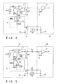
- FIG. 4 shows an embodiment of the present invention using a non-inverting type amplifier as an analog amplifier.
- the signal eil is supplied to a non-inverting input terminal of an operational amplifier 41.
- An output terminal of the operational amplifier 41 is connected to the input terminal of the analog amplifier 2 of the second circuit system 12.
- One end of a resistor R41 is connected to the non-inverting input terminal of the operational amplifier 41 and one end of a resistor R42.
- the other end of the resistor R42 is connected to the output terminal of the operational amplifier 41.
- the reference potential 14 of the second circuit system 12 is supplied to the input terminal IN of the canceling circuit 3.
- the input terminal IN of the canceling circuit 3 is connected to one end of a resistor R43, and the other end of the resistor R43 is connected to the inverting input terminal of the operational amplifier 42.
- the output terminal of the operational amplifier 42 is connected to one end of a resistor R44, and the other end of the resistor R44 is connected to the inverting input terminal of the operational amplifier 42.
- a non-inverting input terminal of the operational amplifier 42 is connected to the reference potential 13 of the first circuit system 11.
- the output terminal of the operational amplifier 42 that is, the output terminal OUT of the canceling circuit 3 is connected to the other end of the resistor R41.
- the operational amplifier 42 serves as a buffer amplifier for supplying an output of Vx times (-R44/R43) at a low impedance to the output terminal OUT of the reference potential difference canceling circuit 3.
- the signal can be received and transmitted between the different circuit systems without generating the noise component.
- the amplifier for generating a differential signal and the amplifier for receiving the differential signal are not needed, so that the manufacturing cost and the circuit occupying area can be reduced.
- FIG. 5 is an embodiment of the present invention showing a case in which the circuit of FIG. 4 is ]operated by a single power supply.
- a non-inverting type amplifier is used as the analog amplifier 1.
- the signal eil is supplied to a non-inverting input terminal of an operational amplifier 51.
- a inverting input terminal of the operational amplifier 51 is connected to one end of the resistor R41, and the other end of the resistor R41 is connected to the output terminal OUT of the canceling circuit 3.
- the inverting input terminal of the operational amplifier 51 is connected to one end of the resistor R42, and the other end of the resistor R42 is connected to the output terminal of the operational amplifier 51.
- the output terminal of the operational amplifier 51 is connected to the input terminal of the analog amplifier 2 of the second circuit system through the coupling condenser C1.
- the input terminal IN of the canceling circuit 3 is connected to the reference potential 14 of the second circuit system through the coupling condenser C2.
- the input terminal IN of the canceling circuit 3 is connected to one end of the resistor R43, and the other end of the resistor R43 is connected to the inverting input terminal of an operational amplifier 52.
- the inverting input terminal of the operational amplifier 52 is connected to one end of the resistor R44, and the other end of the resistor R44 is connected to the output terminal of the operational amplifier 52.
- a non-inverting input terminal of the operational amplifier 52 is connected to another reference potential Vref having a constant potential difference to the reference potential 13 of the first circuit system.
- the reference potential Vref is supplied from a voltage divider using the power supply potential VDD and the reference potential 13 or using the constant power supply.
- the canceling circuit 3 is also used as Vref generator.
- the signal can be received and transmitted between the different circuit systems without generating the noise component.
- the amplifier for generating a differential signal and the amplifier for receiving the differential signal are not needed, so that the manufacturing cost and the circuit occupying area can be reduced.
- the reference potential difference canceling circuit is also used as the Vref generator in operating the amplifier by the single power supply. As a result, increase in the number of parts can be prevented.
- FIG. 6 is an embodiment showing a case of using a differential amplifier as the analog amplifier 1.
- the signal ei- is supplied to one end of a resistor R61, and the other end of the resistor R61 is connected to an inverting input terminal of an operational amplifier 61.
- the inverting input terminal of the operational amplifier 61 is connected to one end of a resistor R62, and the other end of the resistor R62 is connected to the output of the operational amplifier 61.
- the signal ei+ is supplied to one end of a resistor R63, and the other end of the resistor R63 is connected to the non-inverting input terminal of the operational amplifier 61.
- the output terminal of the operational amplifier 61 is connected to the input terminal of the analog amplifier 2 of the second circuit system 12.
- the reference potential 14 of the second circuit system is supplied to the input terminal IN of the canceling circuit 3 of the first circuit system 11.
- the canceling circuit 3 comprises a resistor R64, and R65. One end of the resistor R64 is connected to the input terminal IN of the canceling circuit 3, and the other end of the resistor R64 is connected to the output terminal OUT of the canceling circuit 3. One end of a resistor R65 is connected to the other end of the resistor R64, and the reference potential 13 of the first circuit system is supplied to the other end of the resistor R65.
- the output terminal OUT of the canceling circuit 3 is connected to the non-inverting input terminal of the operational amplifier 61.
- R63'/(R63' + R64) R61/(R61 + R62) may be established.
- the signal can be received and transmitted between the different circuit systems without generating the noise component.
- the amplifier for generating a differential signal and the amplifier for receiving the differential signal are not needed, so that the manufacturing cost and the circuit occupying area can be reduced.
- FIG. 7 is an embodiment showing a case in which the circuit of FIG. 6 is operated by a single power supply.
- the differential analog amplifier 1 is the same as the differential analog amplifier of FIG. 6.
- An output terminal of an operational amplifier 71 is connected to the input terminal of the analog amplifier 2 of the second circuit 12 of the second circuit system 12 through the coupling condenser C1.
- the reference potential 14 of the second circuit system is supplied to the input terminal IN of the canceling circuit 3 through the coupling condenser C2.
- the canceling circuit 3 comprises resistors R64, R65, and R66. Power potential VDD of the first circuit system is supplied to one end of the resistor R66, and the other end of the resistor R66 is connected to the output terminal OUT of the canceling circuit 3. One end of the resistor R65 is connected to the other end of the resistor R66, and the reference potential 13 of the first circuit system 1 is supplied to the other end of the resistor R65. One end of the resistor R64 is connected to the input terminal IN of the canceling circuit 3, and the other end of the resistor R64 is connected to the connection point between the resistors R65 and R66. The output terminal OUT of the canceling circuit 3 is connected to a non-inverting input terminal of an operational amplifier 71.
- the resistor R65 of FIG. 6 is replaced with R65 ⁇ R66/(R65 + R66), so that the resistance condition for canceling Vx can be obtained. Similar to the embodiments of FIGS. 3 and 5, the canceling circuit 3 of this embodiment is also used as a Vref generator.
- the signal can be received and transmitted between the different circuit systems without generating the noise component.
- the amplifier for generating a differential signal and the amplifier for receiving the differential signal are not needed, so that the manufacturing cost and the circuit occupying area can be reduced.
- the reference potential difference canceling circuit is also used as the Vref generator in operating the amplifier by the single power supply. As a result, increase in the number of parts can be prevented.
- FIG. 8 is an embodiment showing a case in which a line for connecting the input terminal IN of the canceling circuit 3 to the second reference potential of the second circuit system is shared when the circuit shown in FIG. 3 is provided for two channels.
- analog amplifiers 1a and 1b and canceling circuits 3a and 3b which are similar to those shown in FIG. 3, are provided in the first circuit system 11.
- the output signals of the analog amplifiers 1a and 1b are supplied to the input analog amplifiers 2a and 2b of the second circuit system 12 through coupling condensers C1a and C1b, respectively.
- the input terminals IN of the canceling circuits 3a and 3b are connected to the reference potential 14 of the second circuit system 12 through a common coupling condenser C2.
- the signal can be received and transmitted between the different circuit systems without generating the noise component.
- the number of condenser C2 for cutting the DC component can be one, so that the number of signals lines and the number of parts of the circuit can be reduced.
- the input signal line for the canceling circuit can be shared.
- FIG. 8 shows the case of the single power supply. However, even in the case of two power supplies as shown in FIG. 2, the connection line between the canceling circuit and the reference potential of the second circuit system can be shared.
- FIG. 9 is an embodiment of the present invention showing a case in which an input signal line of the canceling circuit 3 is shared when the circuit shown in FIG. 5 is provided for two channels.
- two analog amplifiers 1a and 1b which are the same as described in FIG. 5, and two reference potential difference canceling circuits 3a and 3b, which are the same as described in FIG. 5, are provided.
- the output signals of analog amplifiers la and 1b are supplied to input amplifiers 2a and 2b of the second circuit system through coupling condenser C1a and C1b, respectively.
- the input terminal IN of each of the canceling circuits 3a and 3b is connected to the reference potential 14 of the second circuit system through the common condenser C2.
- the signal can be received and transmitted between the different circuit systems without generating the noise component. Similar to the embodiment of FIG. 8, the increase in the number of signal lines and the number of parts can be prevented.
- the input signal line of the canceling circuit 3 can be used as a common input signal line.
- connection line between the input terminal of the canceling circuit 3 and the reference potential of the second circuit system can be used as a common connection line.
- FIG. 10 shows an embodiment in which the reference potential difference canceling circuit 3 is used as a common circuit when the circuit shown in FIG. 3 is provided for two channels.
- one canceling circuit 3 which is the same as shown in FIG. 3, and two inverting type analog amplifiers 1a and 1b, which are the same as shown in FIG. 3, are provided.
- the output signals of the analog amplifiers 1a and 1b are supplied to the input amplifiers 2a and 2b of the second circuit system through the coupling condensers C1a and C1b, respectively.
- the input terminal IN of the canceling circuit 3 is connected to the reference potential 14 of the second circuit system through the coupling condenser C2.
- the output terminal OUT of the canceling circuit 3 is connected to the non-inverting input terminal of the operational amplifier 21a of the analog amplifier la and the non-inverting input terminal of the operational amplifier 21b of the analog amplifier 1b.
- the signal can be received and transmitted between the different circuit systems without generating the noise component.
- the number of parts can be more reduced than the embodiment of FIG. 8.
- the canceling circuit 3 can be used as a common circuit.
- FIG. 10 showed the case of the single power supply. However, even in the case of two power supplies as shown in FIG. 2, the canceling circuit 3 can be used as a common circuit.
- FIG. 11 shows an embodiment of the present invention in which the reference potential difference canceling circuit 3 is used as a common circuit when the circuit shown in FIG. 5 is provided for two channels.
- one canceling circuit 3 which is the same as shown in FIG. 5, and two inverting type analog amplifiers 1a and 1b, which are the same as shown in FIG. 5, are provided.
- the output signals of the analog amplifiers 1a and 1b are supplied to the input amplifiers 2a and 2b of the second circuit system 12 through the coupling condensers C1a and C1b, respectively.
- the input terminal IN of the canceling circuit 3 is connected to the second reference potential of the second circuit system through the coupling condenser C2.
- the output terminal OUT of the canceling circuit 3 is connected to each of the inverting input terminals of operational amplifiers 51a and 51b through each of resistors R41a and R41b.
- the signal can be received and transmitted between the different circuit systems without generating the noise component.
- the number of parts can be more reduced than the embodiment of FIG. 9.
- the canceling circuit 3 can be used as a common circuit.
- FIG. 11 showed the case of the single power supply. However, even in the case of two power supplies as shown in FIG. 4, the canceling circuit 3 can be used as a common circuit.
- FIG. 12 shows an analog amplifier using a switched capacitor.
- the switched capacitor comprises a capacitor C, a switch SWa and a switch SWb.
- the switch SWa has a movable contact, which is connected to the first terminal of the capacitor C, and a fixed contact, which is connected to a terminal a and the reference potential.
- the switch SWb has a movable contact, which is connected to the second terminal of the capacitor C, and a fixed contact, which is connected to a terminal b and the reference potential.
- T shows a period of the opening and closing of each of SWa and SWb.
Landscapes
- Engineering & Computer Science (AREA)
- Power Engineering (AREA)
- Amplifiers (AREA)
- Signal Processing Not Specific To The Method Of Recording And Reproducing (AREA)
- Circuit For Audible Band Transducer (AREA)
Claims (7)
- Ein Verstärker, umfassend:ein erstes Schaltungssystem (11) mit einem analogen Verstärker (1) zum Verstärken eines Übertragungssignals (eil), basierend auf einem Referenzpotential (13) des ersten Schaltungssystems;ein zweites Schaltungssystem (12) zum Empfangen eines Ausgangssignals des analogen Verstärkers (1), basierend auf einem Referenzpotential (14) des zweiten Schaltungssystems; undeine Referenzpotential-Unterschiedsauslösch-Schaltung (3), wobei das Referenzpotential (14) des zweiten Schaltungssystems zugeführt wird, an einen Eingangsanschluss (IN) der Referenzpotential-Unterschiedsauslösch-Schaltung (3), ein Ausgangssignal der Referenzpotential-Unterschiedsauslösch-Schaltung (3) an den Eingangsanschluss des analogen Verstärkers (1) zusammen mit dem Übertragungssignal zugeführt wird, und eine Verstärkung von dem Eingangsanschluss (IN) der Referenzpotential-Unterschiedsauslösch-Schaltung (3) an einen Ausgangsanschluss des analogen Verstärkers (1) 1 ist, und der analoge Verstärker (1) umfasst:einen ersten Operationsverstärker (41) mit einem nicht-invertierenden Eingangsanschluss, an den das Übertragungssignal (ei1) zugeführt wird;einen ersten Widerstand (R41), der ein Ende mit dem invertierenden Eingangsanschluss des ersten Operationsverstärkers (41) verbunden hat; undeinen zweiten Widerstand (R42), der ein Ende mit dem invertierenden Eingangsanschluss des ersten Operationsverstärkers (41) verbunden hat, und das andere Ende mit einem Ausgangsanschluss des ersten Operationsverstärkers (41) verbunden ist;dadurch gekennzeichnet, dass die Referenzpotential-Unterschiedsauslösch-Schaltung (3) umfasst:einen zweiten Operations-(42)-Verstärker mit einem nicht-invertierenden Eingangsanschluss, an den das Referenzpotential (13) des ersten Schaltungssystems zugeführt wird, und einem Ausgangsanschluss verbunden mit dem anderen Ende des ersten Widerstands (R41);einen dritten Widerstand (R43), der ein Ende mit dem Eingangsanschluss (IN) der Referenzpotential-Unterschiedsauslösch-Schaltung verbunden hat, und das andere Ende mit dem invertierenden Eingangsanschluss des zweiten Operationsverstärkers (42) verbunden ist; undeinen vierten Widerstand (R44) der ein Ende mit dem invertierenden Eingangsanschluss des zweiten Operationsverstärkers (42) verbunden hat, und das andere Ende mit dem Ausgangsanschluss des zweiten Operationsverstärkers (42) verbunden ist.
- Ein Verstärker, umfassend:ein erstes Schaltungssystem (11) mit einem analogen Verstärker (1) zum Verstärken eines Übertragungssignals (eil), basierend auf einem Referenzpotential (13) des ersten Schaltungssystems;ein zweites Schaltungssystem (12) zum Empfangen eines Ausgangssignals des analogen Verstärkers (1), basierend auf einem Referenzpotential (14) des zweiten Schaltungssystems; undeine Referenzpotential-Unterschiedsauslösch-Schaltung (3), wobei das Referenzpotential (14) des zweiten Schaltungssystems zugeführt wird an einen Eingangsanschluss (IN) der Referenzpotential-Unterschiedsauslösch-Schaltung, ein Ausgangssignal der Referenzpotential-Unterschiedsauslösch-Schaltung zugeführt wird an den Eingangsanschluss des analogen Verstärkers (1) zusammen mit dem Übertragungssignal, und eine Verstärkung von dem Eingangsanschluss (IN) der Referenzpotential-Unterschiedsauslösch-Schaltung an einen Ausgangsanschluss des analogen Verstärkers (1) 1 ist;wobei der analoge Verstärker (1) umfasst:einen ersten Operationsverstärker (51) mit einem nicht-invertierenden Eingangsanschluss, an den das Übertragungssignal (ei1) zugeführt wird;einen ersten Widerstand (R41), der ein Ende mit dem invertierenden Eingangsanschluss des ersten Operationsverstärkers (51) verbunden hat; undeinen zweiten Widerstand (R42), der ein Ende mit dem invertierenden Eingangsanschluss des ersten Operationsverstärkers (51) verbunden hat, und das andere Ende mit einem Ausgangsanschluss des ersten Operationsverstärkers (51) verbunden ist;dadurch gekennzeichnet, dass die Referenzpotential-Unterschiedsauslösch-Schaltung (3) umfasst:einen zweiten Operations-Verstärker (52) mit einem nicht-invertierenden Eingangsanschluss, an den ein drittes Referenzpotential (Vref) mit einem konstanten Potential zu dem Referenzpotential (13) des ersten Schaltungssystems zugeführt wird, und einem Ausgangsanschluss verbunden mit dem anderen Ende des ersten Widerstands (R41);einen dritten Widerstand (R43), der ein Ende mit einem Eingangsanschluss (IN) der Referenzpotential-Unterschiedsauslösch-Schaltung verbunden hat, und das andere Ende mit einem invertierenden Eingangsanschluss des zweiten Operationsverstärkers (52) verbunden ist; undeinen vierten Widerstand (R44) der ein Ende mit dem invertierenden Eingangsanschluss des zweiten Operationsverstärkers 52) verbunden hat, und das andere Ende mit dem Ausgangsanschluss des zweiten Operationsverstärkers (52) verbunden ist.
- Der Verstärker nach Anspruch 1 oder 2, dadurch gekennzeichnet, dass die Referenzpotential-Unterschiedsauslösch-Schaltung (3) auch als ein Referenzgleichstrompotentialgenerator eines einzelnen Leistungsversorgungsverstärkers verwendet wird.
- Der Verstärker nach Anspruch 2, dadurch gekennzeichnet, dass der Ausgangsanschluss des analogen Verstärkers (1) des ersten Schaltungssystems und der Eingangsanschluss des zweiten Schaltungssystems (12) durch einen Koppelkondensator (C1) verbunden sind; und
der Eingangsanschluss (IN) der Referenzpotential-Unterschiedsauslösch-Schaltung (3) und das Referenzpotential (14) des zweiten Schaltungssystems durch den Koppelkondensator (C2) verbunden sind. - Der Verstärker nach Anspruch 1 oder 2, dadurch gekennzeichnet, dass sowohl der erste als auch der zweite Widerstand einen geschalteten Kondensator umfassen.
- Der Verstärker nach einem der vorhergehenden Ansprüche, dadurch gekennzeichnet, dass eine Mehrzahl der analogen Verstärker (1a, 1b) bereitgestellt wird;
die Referenzpotential-Unterschiedsauslösch-Schaltung (3a, 3b) bereitgestellt wird in jedem der Mehrzahl der analogen Verstärker einer nach dem andern; und
und der Eingangsanschluss von jeder der Referenzpotential-Unterschiedsauslösch-Schaltungen verbunden ist mit dem Referenzpotential des zweiten Schaltungssystems durch eine gemeinsame Signalleitung. - Der Verstärker nach einem der Ansprüche 1 bis 5, dadurch gekennzeichnet, dass eine Mehrzahl der analogen Verstärker (1a, 1b) bereitgestellt wird; und
eine gemeinsame Referenzpotential-Unterschiedsauslösch-Schaltung (3) bereitgestellt wird für jeden der Mehrzahl der analogen Verstärker.
Applications Claiming Priority (3)
| Application Number | Priority Date | Filing Date | Title |
|---|---|---|---|
| JP12464996A JP3410901B2 (ja) | 1996-05-20 | 1996-05-20 | 増幅回路 |
| JP12464996 | 1996-05-20 | ||
| JP124649/96 | 1996-05-20 |
Publications (3)
| Publication Number | Publication Date |
|---|---|
| EP0809353A2 EP0809353A2 (de) | 1997-11-26 |
| EP0809353A3 EP0809353A3 (de) | 1999-07-14 |
| EP0809353B1 true EP0809353B1 (de) | 2006-06-21 |
Family
ID=14890640
Family Applications (1)
| Application Number | Title | Priority Date | Filing Date |
|---|---|---|---|
| EP97107186A Expired - Lifetime EP0809353B1 (de) | 1996-05-20 | 1997-04-30 | Verstärker zur Unterdrückung von Störgeräusch zwischen Schaltungssystemen |
Country Status (6)
| Country | Link |
|---|---|
| US (1) | US5841308A (de) |
| EP (1) | EP0809353B1 (de) |
| JP (1) | JP3410901B2 (de) |
| KR (1) | KR100253727B1 (de) |
| DE (1) | DE69736153T2 (de) |
| TW (1) | TW350171B (de) |
Families Citing this family (17)
| Publication number | Priority date | Publication date | Assignee | Title |
|---|---|---|---|---|
| US6040728A (en) * | 1998-05-29 | 2000-03-21 | Lucent Technologies, Inc. | Active substrate noise injection cancellation |
| FR2793622B1 (fr) * | 1999-05-10 | 2004-03-12 | Peugeot Citroen Automobiles Sa | Dispositif de raccordement d'une source a un equipement de diffusion audiophonique notamment d'un vehicule automobile |
| US6208190B1 (en) * | 1999-05-27 | 2001-03-27 | Lucent Technologies Inc. | Minimizing effects of switching noise in mixed signal chips |
| JP3666317B2 (ja) * | 1999-09-07 | 2005-06-29 | セイコーエプソン株式会社 | 送信回路、受信回路、送受信回路および電気光学装置 |
| EP1220444A1 (de) * | 2000-12-28 | 2002-07-03 | Alcatel | Differenzausgangsverstärkeranordnung |
| EP1568159A1 (de) * | 2002-11-28 | 2005-08-31 | Koninklijke Philips Electronics N.V. | Unterdrückung von störungen in einer integrierten schaltung |
| US6937099B2 (en) * | 2003-12-04 | 2005-08-30 | Analog Devices, Inc. | Op-amp configurable in a non-inverting mode with a closed loop gain greater than one with output voltage correction for a time varying voltage reference of the op-amp, and a method for correcting the output voltage of such an op-amp for a time varying voltage reference |
| US6958642B2 (en) * | 2003-12-19 | 2005-10-25 | Caterpillar Inc | Ground difference compensating system |
| EP2022167B1 (de) * | 2006-05-16 | 2010-12-15 | Freescale Semiconductor, Inc. | Verstärkerschaltung und integrierte schaltung dafür |
| US7391348B2 (en) * | 2006-10-23 | 2008-06-24 | Agere Systems Inc. | Reducing noise associated with local reference-potential fluctuations in mixed-signal integrated circuits |
| CA2623061A1 (en) * | 2007-03-02 | 2008-09-02 | Sean C. Carroll | Zero crossing circuit |
| US7944290B2 (en) * | 2009-01-26 | 2011-05-17 | Sumitomo Electric Industries, Ltd. | Trans-impedance amplifier |
| JP5517777B2 (ja) * | 2010-06-25 | 2014-06-11 | 日立オートモティブシステムズ株式会社 | ブリッジ回路の断線検出回路および断線検出手段を有するシステム |
| US9151783B2 (en) | 2012-04-26 | 2015-10-06 | Synopsys, Inc. | Ground offset monitor and compensator |
| JP6027444B2 (ja) * | 2013-01-07 | 2016-11-16 | ローム株式会社 | オーディオ信号処理回路およびそれを用いた車載用オーディオ装置、オーディオコンポーネント装置、電子機器 |
| CN109072338A (zh) * | 2016-05-16 | 2018-12-21 | 捷客斯金属株式会社 | 稀有金属回收方法 |
| EP3667907B1 (de) | 2018-12-14 | 2022-09-14 | Stichting IMEC Nederland | Ausleseschaltung zum erfassen eines mehrkanaligen biopotentialsignals und sensor zum erfassen eines biopotentialsignals |
Family Cites Families (7)
| Publication number | Priority date | Publication date | Assignee | Title |
|---|---|---|---|---|
| DE2830033A1 (de) * | 1978-07-07 | 1980-01-17 | Hellige Gmbh | Verstaerkeranordnung mit stoersignalunterdrueckung |
| JPS59200508A (ja) * | 1983-04-26 | 1984-11-13 | Pioneer Electronic Corp | 増幅器 |
| JP3167319B2 (ja) * | 1990-10-25 | 2001-05-21 | パイオニア株式会社 | アイソレータ回路 |
| JP2516706B2 (ja) * | 1990-11-24 | 1996-07-24 | ローム株式会社 | アンプ |
| US5648738A (en) * | 1994-11-01 | 1997-07-15 | Cirrus Logic, Inc. | Read channel having auto-zeroing and offset compensation, and power-down between servo fields |
| US5661423A (en) * | 1995-12-14 | 1997-08-26 | Lucent Technologies Inc. | High speed comparator circuits with offset voltage compensation |
| US5606273A (en) * | 1996-03-28 | 1997-02-25 | Caterpillar Inc. | Zero crossing detector circuit |
-
1996
- 1996-05-20 JP JP12464996A patent/JP3410901B2/ja not_active Expired - Fee Related
-
1997
- 1997-04-29 US US08/848,269 patent/US5841308A/en not_active Expired - Lifetime
- 1997-04-30 DE DE69736153T patent/DE69736153T2/de not_active Expired - Lifetime
- 1997-04-30 EP EP97107186A patent/EP0809353B1/de not_active Expired - Lifetime
- 1997-05-09 TW TW086106204A patent/TW350171B/zh not_active IP Right Cessation
- 1997-05-16 KR KR1019970018859A patent/KR100253727B1/ko not_active Expired - Fee Related
Also Published As
| Publication number | Publication date |
|---|---|
| DE69736153T2 (de) | 2007-05-03 |
| TW350171B (en) | 1999-01-11 |
| KR970078028A (ko) | 1997-12-12 |
| EP0809353A3 (de) | 1999-07-14 |
| JPH09312525A (ja) | 1997-12-02 |
| KR100253727B1 (ko) | 2000-04-15 |
| US5841308A (en) | 1998-11-24 |
| DE69736153D1 (de) | 2006-08-03 |
| JP3410901B2 (ja) | 2003-05-26 |
| EP0809353A2 (de) | 1997-11-26 |
Similar Documents
| Publication | Publication Date | Title |
|---|---|---|
| EP0809353B1 (de) | Verstärker zur Unterdrückung von Störgeräusch zwischen Schaltungssystemen | |
| EP0151014B1 (de) | Radio-Sender-Empfänger mit einer umschaltbaren Antennenkopplungsschaltung | |
| EP1024613A3 (de) | Umsetzer für Satellitenrundfunksignale mit mehreren Ausgängen | |
| WO2001047109A3 (en) | Low voltage differential signal (lvds) input circuit | |
| JP3189546B2 (ja) | 送受信回路 | |
| JPH07235952A (ja) | 信号伝送回路およびその回路を用いた信号伝送装置 | |
| EP0797210A3 (de) | Ausgangpufferschaltung | |
| US5317597A (en) | Resistance coupled data transmission arrangement | |
| EP1098412A3 (de) | Schutzschalter mit programmierbarem Verstärker | |
| US5485302A (en) | Optical receiver with signal splitter | |
| EP0868035A2 (de) | Analoger Signalübertragungskreis | |
| JPH07212257A (ja) | 送信機の異常送信停止回路 | |
| EP0114320B1 (de) | Offsetspannungsschaltung zur Anwendung mit einem Leitungsempfänger oder dergleichen | |
| US7161419B2 (en) | Sensor device and a signal amplification device of a small detection signal provided by the sensor | |
| US6426970B1 (en) | Bi-directional signal coupler method and apparatus | |
| EP0124315B1 (de) | Verstärker | |
| EP0778671A3 (de) | Hochfrequenzschalter | |
| EP0583398A4 (en) | Drive amplifier for power line communications | |
| JPH0624327B2 (ja) | 端末装置 | |
| US20030081663A1 (en) | Interface circuit of differential signaling system | |
| EP1481488B1 (de) | Sender/empfaenger für die bidirektionale kommunikation | |
| EP0473165B1 (de) | Gegentakt-Leistungsverstärker | |
| JP3377801B2 (ja) | 高周波信号切換回路 | |
| JPH0572139B2 (de) | ||
| KR100208208B1 (ko) | 무선통신기기에서 반이중 통신용 입출력 분리회로 |
Legal Events
| Date | Code | Title | Description |
|---|---|---|---|
| PUAI | Public reference made under article 153(3) epc to a published international application that has entered the european phase |
Free format text: ORIGINAL CODE: 0009012 |
|
| 17P | Request for examination filed |
Effective date: 19970430 |
|
| AK | Designated contracting states |
Kind code of ref document: A2 Designated state(s): DE FR GB |
|
| PUAL | Search report despatched |
Free format text: ORIGINAL CODE: 0009013 |
|
| AK | Designated contracting states |
Kind code of ref document: A3 Designated state(s): DE FR GB |
|
| 17Q | First examination report despatched |
Effective date: 20010326 |
|
| GRAP | Despatch of communication of intention to grant a patent |
Free format text: ORIGINAL CODE: EPIDOSNIGR1 |
|
| GRAS | Grant fee paid |
Free format text: ORIGINAL CODE: EPIDOSNIGR3 |
|
| GRAA | (expected) grant |
Free format text: ORIGINAL CODE: 0009210 |
|
| AK | Designated contracting states |
Kind code of ref document: B1 Designated state(s): DE FR GB |
|
| REG | Reference to a national code |
Ref country code: GB Ref legal event code: FG4D |
|
| REF | Corresponds to: |
Ref document number: 69736153 Country of ref document: DE Date of ref document: 20060803 Kind code of ref document: P |
|
| PLBE | No opposition filed within time limit |
Free format text: ORIGINAL CODE: 0009261 |
|
| STAA | Information on the status of an ep patent application or granted ep patent |
Free format text: STATUS: NO OPPOSITION FILED WITHIN TIME LIMIT |
|
| EN | Fr: translation not filed | ||
| 26N | No opposition filed |
Effective date: 20070322 |
|
| GBPC | Gb: european patent ceased through non-payment of renewal fee |
Effective date: 20070430 |
|
| PG25 | Lapsed in a contracting state [announced via postgrant information from national office to epo] |
Ref country code: GB Free format text: LAPSE BECAUSE OF NON-PAYMENT OF DUE FEES Effective date: 20070430 Ref country code: FR Free format text: LAPSE BECAUSE OF FAILURE TO SUBMIT A TRANSLATION OF THE DESCRIPTION OR TO PAY THE FEE WITHIN THE PRESCRIBED TIME-LIMIT Effective date: 20070309 |
|
| PG25 | Lapsed in a contracting state [announced via postgrant information from national office to epo] |
Ref country code: FR Free format text: LAPSE BECAUSE OF FAILURE TO SUBMIT A TRANSLATION OF THE DESCRIPTION OR TO PAY THE FEE WITHIN THE PRESCRIBED TIME-LIMIT Effective date: 20060621 |
|
| PGFP | Annual fee paid to national office [announced via postgrant information from national office to epo] |
Ref country code: DE Payment date: 20120502 Year of fee payment: 16 |
|
| PG25 | Lapsed in a contracting state [announced via postgrant information from national office to epo] |
Ref country code: DE Free format text: LAPSE BECAUSE OF NON-PAYMENT OF DUE FEES Effective date: 20131101 |
|
| REG | Reference to a national code |
Ref country code: DE Ref legal event code: R119 Ref document number: 69736153 Country of ref document: DE Effective date: 20131101 |